-
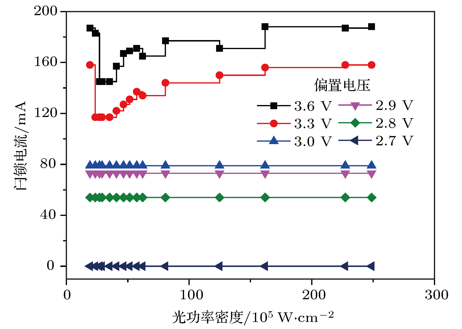
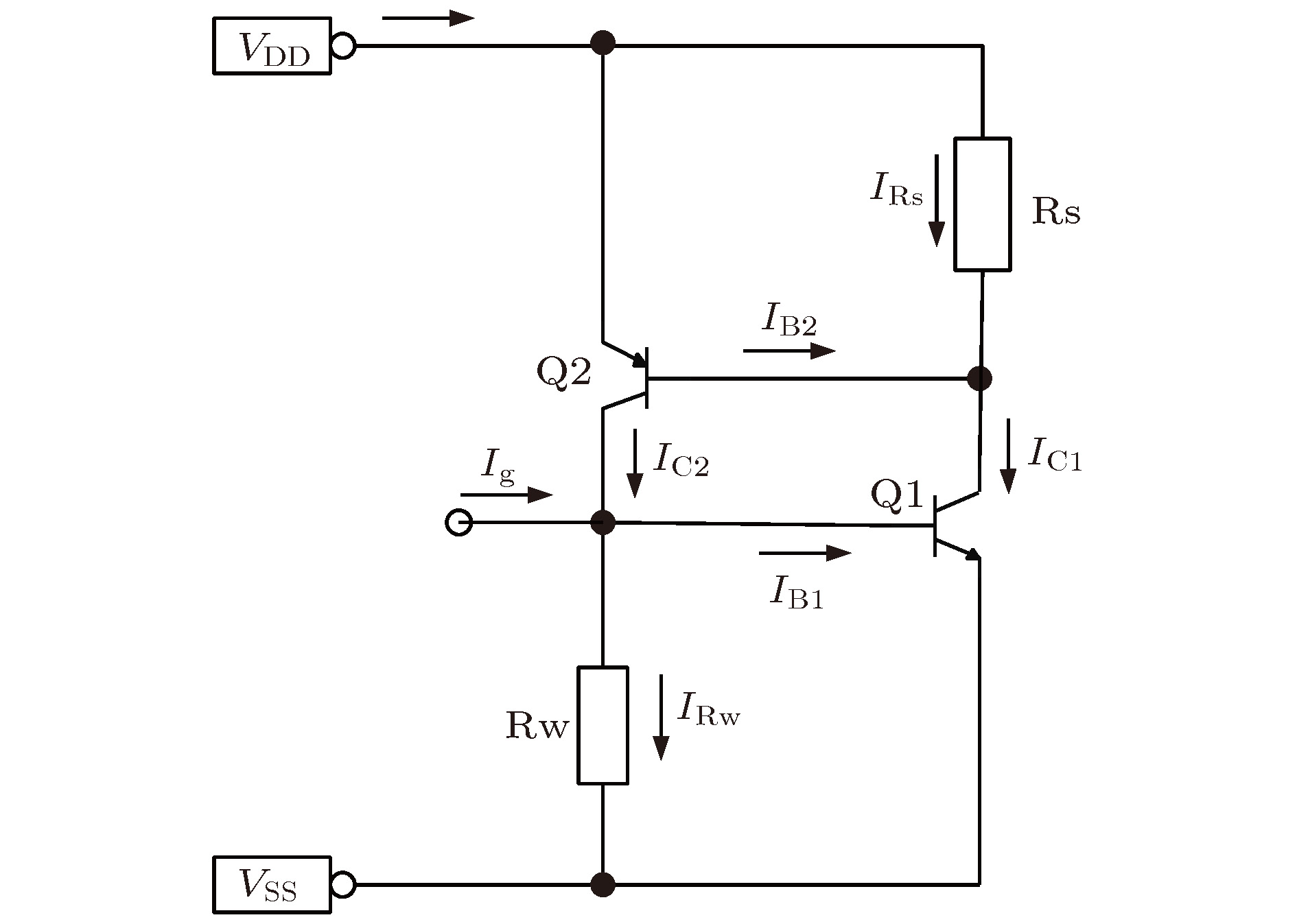
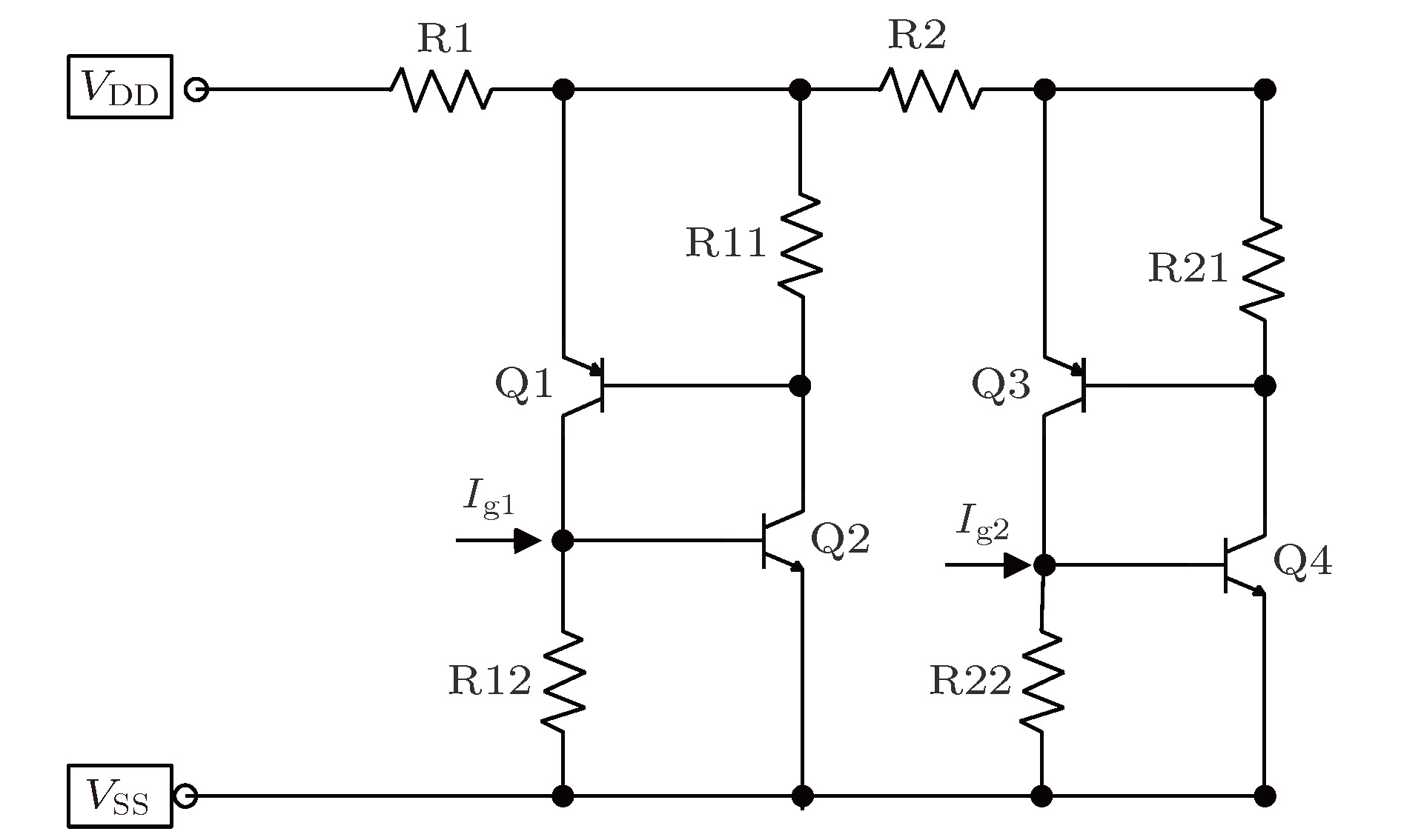
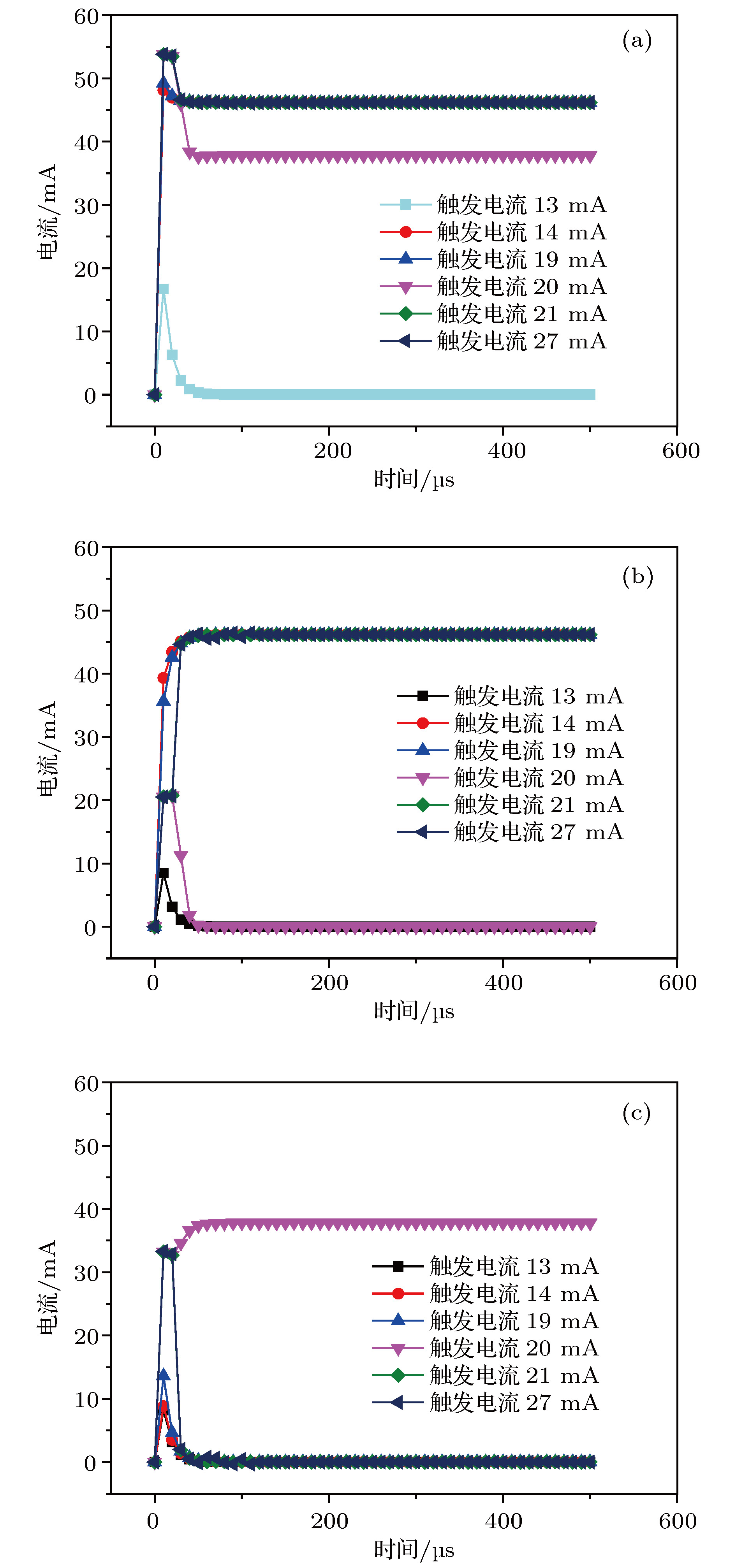
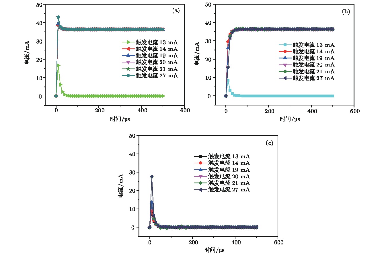
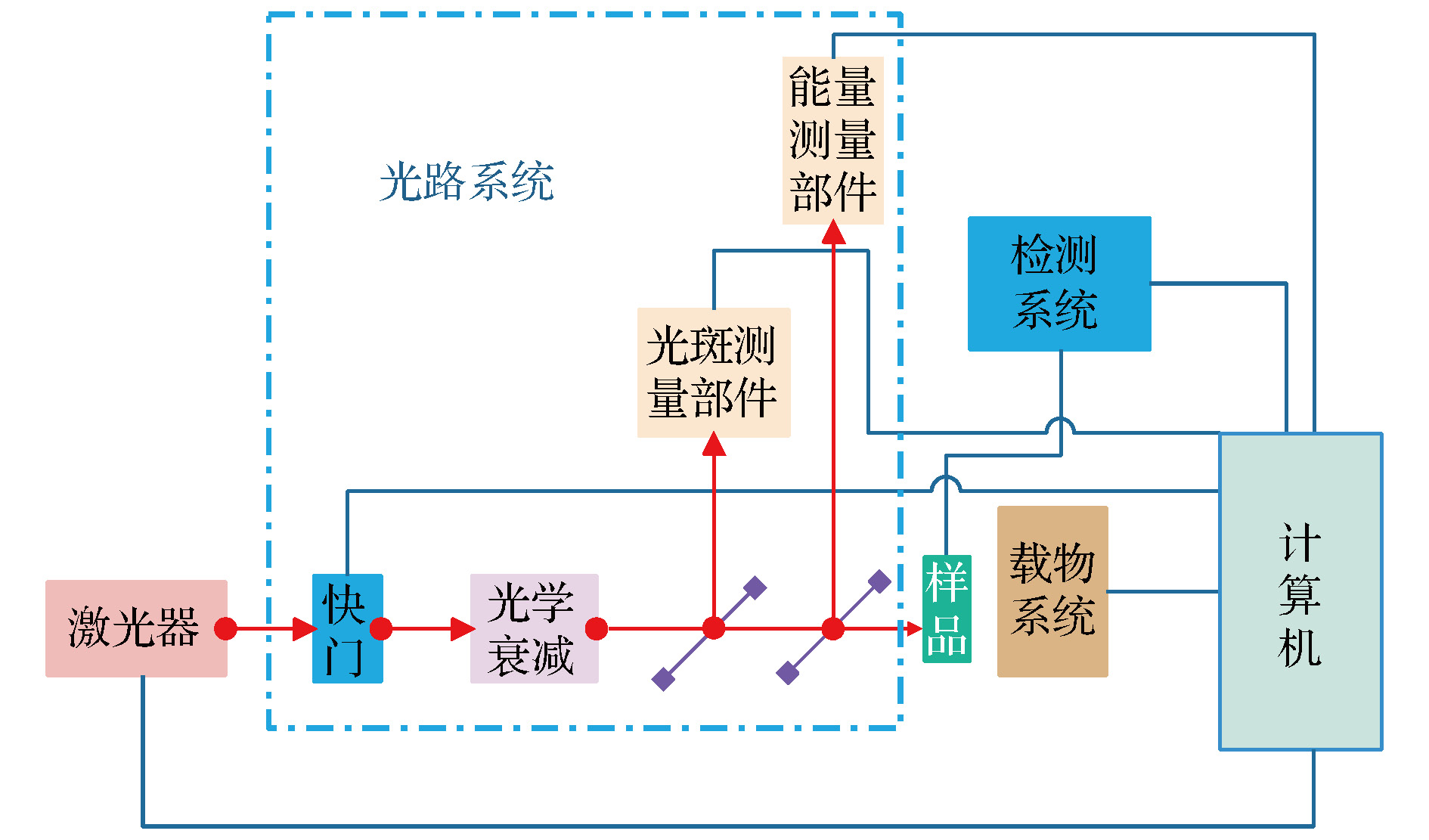
Due to the parasitic PNPN structure, the complementary metal oxide semiconductor (CMOS) integrated circuit may be affected by the latch-up effect, and the latching induced by the transient high dose rate Gamma ray has unique characteristics. In order to explore the complex physical mechanism of the latch-up by transient dose rate effect, in this paper we select the pulsed laser with 1064 nm wavelength as an radiation source to simulate the gamma ray radiation environment, select bulk silicon CMOS deserializer FIN1218MTDX, and use transient dose rate effect laser simulation experiments to explore its latch-up threshold and latch-up current characteristics. The test obtains that the dose rate latch-up threshold optical power density of the device at 3.3 V operating voltage is (8.5 ± 1.2) × 104 W/cm2, a latch-up voltage of the device is 2.8 V, only the device latches when the supply voltage is greater than 2.8 V. At the same time, it is found that under the working voltages of 3.3 V and 3.6 V and the optical power density between 1.9 × 10⁶ W/cm2 and 1.6 × 10⁷ W/cm2, the latch-up current significantly decreases, the latch-up current " window phenomenon” appears. Based on the equivalent circuit model, the multi-path latching mechanism is used to construct the HSPICE model. The mechanism of the transient dose rate latching characteristics exposed by the laser test is analyzed by circuit-level simulation. The results show that the latch-up current and the latch-up voltage are related to its own latch structure when the device is latched. The phenomenon of latch-up current window in laser test is due to the multi-path latch mechanism, which will be in the specific circuit structure, and causing the multiple latch-up paths of the device to be switched. The reason of the latch-up path is switched is that the different holding voltages and trigger conditions between the latch-up paths, distributed resistance in the circuit reduces the voltage of latch-up path, so that the holding voltage of the latch-up path cannot be satisfied and the latch-up path is released. At the same time the other latch-up path is latched.
-
Keywords:
- dose rate effect /
- latch-up effect /
- pulsed laser
[1] Marshall R W 1963 Tenth Annual East Coast Conference on Aerospace and Navigational Electronics Baltimore, USA, October 21−23, 1963 p1411
[2] WIrth J L, Rogers S C 1964 IEEE Trans. Nucl. Sci. 11 24
[3] Ellis T D, Kim Y D 1978 IEEE Trans. Nucl. Sci. 25 1489
 Google Scholar
[4] 王桂珍, 林东生, 齐超, 白小燕, 杨善潮, 李瑞宾, 马强, 金晓明, 刘岩 2014 原子能科学技术 48 2165
 Google Scholar
Wang G Z, Lin D S, Qi C, Bai X Y, Yang S C, Li R B, Ma Q, Jin X M, Liu Y 2014 Atom Energ. Sci. Technol. 48 2165
 Google Scholar
[5] 王桂珍, 林东生, 齐超, 白小燕, 杨善潮, 李瑞宾, 马强, 金晓明, 刘岩 2014 微电子学 44 510
Wang G Z, Lin D S, Qi C, Bai X Y, Yang S C, Li R B, Ma Q, Jin X M, Liu Y 2014 Microelectronics 44 510
[6] 梁堃, 孙鹏, 李沫, 代刚, 李顺, 解磊 2017 原子能科学技术 51 187
 Google Scholar
Liang K, Sun P, Li M, Dai G, Li S, Xie L 2017 Atom. Energ. Sci. Technol. 51 187
 Google Scholar
[7] 岳龙, 张战刚, 何玉娟, 郝明明, 雷志峰, 刘远 2017 太赫兹科学与电子信息学报 15 139
 Google Scholar
Yue L, Zhang Z G, He Y J, Hao M M, Lei Z F, Liu Y 2017 J. THZ Sci. Electron. Inform. Technol. 15 139
 Google Scholar
[8] NikZorov A Y, Skorobogatov P K 1996 IEEE Trans. Nucl. Sci. 43 3115
 Google Scholar
[9] Skorobogatov P K, Nikiforov A Y, Demidov A A 1998 IEEE Trans. Nucl. Sci. 45 2659
 Google Scholar
[10] Raburn W D, Buchner S P, Kang K, Singh R, Sayers S 1988 IEEE Trans. Nucl. Sci. 35 1512
 Google Scholar
[11] Johnston A H 1993 IEEE Trans. Nucl. Sci. 40 1694
 Google Scholar
[12] Ochoa A, Dressendorfer P V 1981 IEEE Trans. Nucl. Sci. 28 4292
 Google Scholar
[13] Azarewicz J L, Hardwick W H 1982 IEEE Trans. Nucl. Sci. 29 1803
 Google Scholar
[14] Coppage F N, Allen D J, Dressendorfer P V, Ochoa A, Rauchfuss J, Wrobel T F 1983 IEEE Trans. Nucl. Sci. 30 4122
 Google Scholar
[15] Johnston A H, Baze M P 1985 IEEE Trans. Nucl. Sci. 32 4017
[16] Plaag R E, Baze M P, Johnston A H 1988 IEEE Trans. Nucl. Sci. 35 1563
 Google Scholar
[17] Johnston A H, Plaag R E, Baze M P 1989 IEEE Trans. Nucl. Sci. 36 2229
 Google Scholar
[18] 许献国, 杨怀民, 胡健栋 2004 核电子学与探测技术 24 674
 Google Scholar
Xu X G, Yang H M, Hu J D 2004 Nucl. Electron. Detect. Technol. 24 674
 Google Scholar
[19] 许献国, 徐曦, 胡健栋, 赵汝清 2005 强激光与粒子束 17 633
Xu X G, Xu X, Hu J D, Zhao R Q 2005 High Pow. Las. Part. Beam. 17 633
-
表 1 实验装置技术指标
Table 1. Test equipment technical parameters
装置名称 激光
波长脉冲
宽度最大光斑尺寸 最大
能量重复频率 激光瞬态剂量率辐照装置 1064 nm 10 ns 1 cm 1 J 1—10 Hz 表 2 路径参数
Table 2. Path parameters
表 3 仿真结果表
Table 3. Simulation results table
触发电流/mA 偏置电压5 V 偏置电压6 V 闩锁情况 闩锁路径 闩锁电流/ mA 闩锁情况 闩锁路径 闩锁电流/ mA 13 不闩锁 — — 不闩锁 — — 14 闩锁 路径1 36 闩锁 路径1 46 19 闩锁 路径1 36 闩锁 路径1 46 20 闩锁 路径1 36 闩锁 路径2 38 21 闩锁 路径1 36 闩锁 路径1 46 27 闩锁 路径1 36 闩锁 路径1 46 -
[1] Marshall R W 1963 Tenth Annual East Coast Conference on Aerospace and Navigational Electronics Baltimore, USA, October 21−23, 1963 p1411
[2] WIrth J L, Rogers S C 1964 IEEE Trans. Nucl. Sci. 11 24
[3] Ellis T D, Kim Y D 1978 IEEE Trans. Nucl. Sci. 25 1489
 Google Scholar
[4] 王桂珍, 林东生, 齐超, 白小燕, 杨善潮, 李瑞宾, 马强, 金晓明, 刘岩 2014 原子能科学技术 48 2165
 Google Scholar
Wang G Z, Lin D S, Qi C, Bai X Y, Yang S C, Li R B, Ma Q, Jin X M, Liu Y 2014 Atom Energ. Sci. Technol. 48 2165
 Google Scholar
[5] 王桂珍, 林东生, 齐超, 白小燕, 杨善潮, 李瑞宾, 马强, 金晓明, 刘岩 2014 微电子学 44 510
Wang G Z, Lin D S, Qi C, Bai X Y, Yang S C, Li R B, Ma Q, Jin X M, Liu Y 2014 Microelectronics 44 510
[6] 梁堃, 孙鹏, 李沫, 代刚, 李顺, 解磊 2017 原子能科学技术 51 187
 Google Scholar
Liang K, Sun P, Li M, Dai G, Li S, Xie L 2017 Atom. Energ. Sci. Technol. 51 187
 Google Scholar
[7] 岳龙, 张战刚, 何玉娟, 郝明明, 雷志峰, 刘远 2017 太赫兹科学与电子信息学报 15 139
 Google Scholar
Yue L, Zhang Z G, He Y J, Hao M M, Lei Z F, Liu Y 2017 J. THZ Sci. Electron. Inform. Technol. 15 139
 Google Scholar
[8] NikZorov A Y, Skorobogatov P K 1996 IEEE Trans. Nucl. Sci. 43 3115
 Google Scholar
[9] Skorobogatov P K, Nikiforov A Y, Demidov A A 1998 IEEE Trans. Nucl. Sci. 45 2659
 Google Scholar
[10] Raburn W D, Buchner S P, Kang K, Singh R, Sayers S 1988 IEEE Trans. Nucl. Sci. 35 1512
 Google Scholar
[11] Johnston A H 1993 IEEE Trans. Nucl. Sci. 40 1694
 Google Scholar
[12] Ochoa A, Dressendorfer P V 1981 IEEE Trans. Nucl. Sci. 28 4292
 Google Scholar
[13] Azarewicz J L, Hardwick W H 1982 IEEE Trans. Nucl. Sci. 29 1803
 Google Scholar
[14] Coppage F N, Allen D J, Dressendorfer P V, Ochoa A, Rauchfuss J, Wrobel T F 1983 IEEE Trans. Nucl. Sci. 30 4122
 Google Scholar
[15] Johnston A H, Baze M P 1985 IEEE Trans. Nucl. Sci. 32 4017
[16] Plaag R E, Baze M P, Johnston A H 1988 IEEE Trans. Nucl. Sci. 35 1563
 Google Scholar
[17] Johnston A H, Plaag R E, Baze M P 1989 IEEE Trans. Nucl. Sci. 36 2229
 Google Scholar
[18] 许献国, 杨怀民, 胡健栋 2004 核电子学与探测技术 24 674
 Google Scholar
Xu X G, Yang H M, Hu J D 2004 Nucl. Electron. Detect. Technol. 24 674
 Google Scholar
[19] 许献国, 徐曦, 胡健栋, 赵汝清 2005 强激光与粒子束 17 633
Xu X G, Xu X, Hu J D, Zhao R Q 2005 High Pow. Las. Part. Beam. 17 633
Catalog
Metrics
- Abstract views: 17843
- PDF Downloads: 91
- Cited By: 0


 DownLoad:
