


-
In this paper, a porous silicon-calcium fluoride hybrid plasmonic waveguide (PS-CaF2 HPW) with an asymmetric silver film is studied. The PS-CaF2 HPW is composed of a PS strip waveguide deposited with asymmetric CaF2 and Ag thin film layers on an SiO2 substrate. In the mid-infrared (MIR) region, the mode characteristics and waveguide sensitivity of the mode in the PS-CaF2 HPW are simulated by using the finite element method (FEM). The results show that there are two fundamental modes (PM 1 and PM 2) with different polarization states in the PS-CaF2 HPW. The real part of the effective refractive index (Re(neff
)), transmission loss (α), normalized effective mode field area (A), quality factor (FOM) and sensitivity (Swg) for each of the PM 1 and the PM 2 are studied and optimized. Moreover, the effect of temperature on the performances of the PS-CaF2 HPW is also analyzed. Firstly, the mode field distributions calculated by the FEM indicate that the mode field energy for each of the PM 1 and PM 2 in the PS-CaF2 HPW is mostly restricted to the PS layer and CaF2 layer. Comparing with conventional dielectric waveguides, the mode field energy of the PS-CaF2 HPW is well confined in the PS layer and CaF2 layer. The geometric parameters of the PS-CaF2 HPW are optimized by changing the geometric parameters (W1, W2, and W3). When W1 = 1500 nm, W2 = 300 nm, W3 = 70 nm, and the operating wavelength is ~3.5 μm, α and FOM are 0.019 dB/μm and 1594.99 for the PM 1, and α and FOM are 0.016 dB/μm and 1335.54 for the PM 2, respectively. Secondly, the waveguide sensitivity of the PS-CaF2 HPW is analyzed. The results show that the size of PS layer has a great influence on the waveguide sensitivity. The waveguide sensitivity decreases with the size of the PS layer increasing. In addition, the PS-CaF2 HPW has good temperature resistance. Moreover, temperature has almost no effect on Re(neff ), nor α nor A nor FOM nor Swg in a temperature range from -40 K to 40 K. Finally, the fabrication tolerances of the PS-CaF2 HPW are demonstrated, and the good properties are maintained in a size tolerance range from -10 nm to 10 nm. With the advantages in propagation property and loss reduction, the PS-CaF2 HPW provides a feasible label-free biochemical sensing scheme and a method of polarization control devices. -
Keywords:
- hybrid plasmonic waveguide /
- surface plasmon polaritons /
- propagation property /
- waveguide sensitivity
[1] Oulton R F, Sorger V J, Genov D A, Pile D F P, Zhang X 2008 Nat. Photonics 2 496
 Google Scholar
[2] Burstein E, Chen W P, Chen Y J, Hartstein A 1974 J. Vac. Sci. Technol. 11 1004
Google Scholar
[3] Garcia de Abajo F J, Saenz J J 2005 Phys. Rev. Lett. 95 233901
Google Scholar
[4] Yang L K, Li P, Wang H C, Li Z P 2018 Chin. Phys. B. 27 094216
Google Scholar
[5] Zhang H F, Cao D, Tao F, Yang X H, Wang Y, Yan X N, Bai L H 2010 Chin. Phys. B. 19 027301
Google Scholar
[6] Gong P Q, Li X G, Zhou X, Zhang Y A, Chen N, Wang S K, Zhang S Q, Zhao Y 2021 Opt. Laser Technol. 139 106981
Google Scholar
[7] Smith C L, Thilsted A H, Garcia-Ortiz C E, Radko I P, Marie R, Jeppesen C, Vannahme C, Bozhevolnyi S I, Kristensen A 2014 Nano Lett. 14 1659
Google Scholar
[8] Kumari B, Barh A, Varshney R K, Pal B P 2016 Sens. Actuators, B 236 759
Google Scholar
[9] Kumari B, Varshney R K, Pal B P 2018 Sens. Actuators, B 255 3409
Google Scholar
[10] Mortensen N A, Bozhevolnyi S I, Alù A 2019 Nanophotonics 8 1315
Google Scholar
[11] Nedeljkovic M, Stankovic S, Mitchell C J, Khokhar A Z, Reynolds S A, Thomson D J, Gardes F Y, Littlejohns C G, Reed G T, Mashanovich G Z 2014 IEEE Photonics Technol. Lett. 26 1352
Google Scholar
[12] Shen L, Healy N, Mitchell C J, Penades J S, Nedeljkovic M, Mashanovich G Z, Peacock A C 2015 Opt. Lett. 40 268
Google Scholar
[13] Cheng Z Z, Chen X, Wong C Y, Xu K, Tsang H K 2012 IEEE Photonics J. 4 1510
Google Scholar
[14] Shankar R, Bulu I, Lončar M 2013 Appl. Phys. Lett. 102 051108
Google Scholar
[15] El Shamy R S, Swillam M A, Khalil D A 2019 J. Lightwave Technol. 37 4394
Google Scholar
[16] Alonso-Ramos C, Nedeljkovic M, Benedikovic D, Penades J S, Littlejohns C G, Khokhar A Z, Perez-Galacho D, Vivien L, Cheben P, Mashanovich G Z 2016 Opt. Lett. 41 4324
Google Scholar
[17] Hassan K, Leroy F, Colas-des-Francs G, Weeber J C 2014 Opt. Lett. 39 697
Google Scholar
[18] Dai D X, He S L 2009 Opt. Express 17 16646
Google Scholar
[19] Mai W J, Wang Y L, Zhang Y Y, Cui L N, Yu L 2017 Chin. Phys. B. 34 024204
Google Scholar
[20] 王志斌, 尹少杰, 段晓宁, 邓玉萍, 董伟, 孔祥瑞 2020 中国激光 47 0313001
Google Scholar
Wang Z B, Yin S J, Duan X N, Deng Y P, Dong W, Kong X R 2020 Chin. J. Las. 47 0313001
Google Scholar
[21] Heo J H, Shin D H, Kim S, Jang M H, Lee M H, Seo S W, Choi S H, Im S H 2017 J. Chem. Eng. Jpn. 323 153
Google Scholar
[22] Hwang K W, Park S H 2015 Mater. Res. Innovations 19 S8
Google Scholar
[23] Chen F, Lv H, Pang Z, Zhang J, Hou Y, Gu Y, Yang H, Yang G 2019 IEEE Sens. J. 19 8441
Google Scholar
[24] Olenych I B, Monastyrskii L S, Aksimentyeva O I, Orovcík L, Salamakha M Y 2019 Mol. Cryst. Liq. Cryst. 673 32
Google Scholar
[25] 孙鹏, 胡明, 刘博, 孙凤云, 许路加 2011 物理学报 60 057303
Google Scholar
Sun P, Hu M, Liu B, Sun F Y, Xun L J 2011 Acta. Phys. Sin. 60 057303
Google Scholar
[26] 陈颖, 范卉青, 卢波 2014 物理学报 63 244207
Google Scholar
Chen Y, Fan H Q, Lu B 2014 Acta. Phys. Sin. 63 244207
Google Scholar
[27] Chan K C, Tso C Y, Hussain A, Chao C Y H 2019 Appl. Therm. Eng. 161 114112
Google Scholar
[28] Gan F L, Wang B D, Jin Z H, Xie L L, Dai Z D, Zhou T X, Jiang X 2021 Sci. Total. Environ. 768 144529
Google Scholar
[29] Girault P, Azuelos P, Lorrain N, Poffo L, Lemaitre J, Pirasteh P, Hardy I, Thual M, Guendouz M, Charrier J 2017 Opt. Mater. 72 596
Google Scholar
[30] Palik E D 1985 Academic Press 39 1
[31] Ciminelli C, Campanella C M, Dell’Olio F, Campanella C E, Armenise M N 2013 Prog. Quantum Electron. 37 51
Google Scholar
-

图 1 非对称银膜的PS-CaF2混合等离子体波导示意图 (a)三维图; (b)波导截面图
Figure 1. Schematic diagram of Ag film coated asymmetric PS-CaF2 hybrid plasma waveguide: (a) 3D diagram; (b) cross-sectional view.
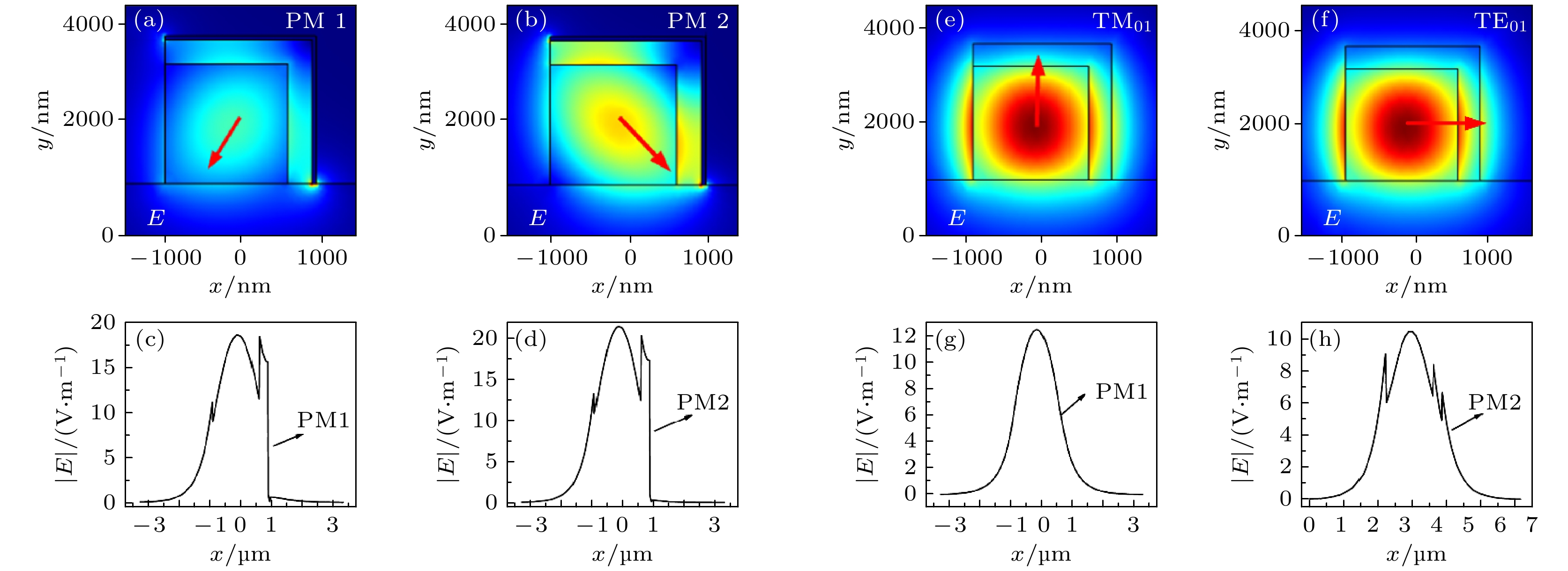
图 2 W1 (= H1) = 1500 nm, W2 (= H2) = 300 nm和W3 (= H3) = 70时, 非对称银膜PS-CaF2混合等离子体波导中不同模式的模场分布图 (a) PM 1; (b) PM 2; 波导中心沿x方向的电场分布图 (c) PM 1; (d) PM 2; W1 (= H1) = 1500 nm和W2 (= H2) = 300 nm时, 无银膜普通波导的模场分布图 (e) TM01; (f) TE01; 波导中心沿x方向的电场分布图 (g) TM01, (h) TE01
Figure 2. Mode field distributions of (a) PM 1 and (b) PM 2; electric field distribution along the x axis of (c) PM 1 and (d) PM 2; mode field distributions of (e) TM01 and (f) TE01; electric field distribution along the x axis of (g) TM01 and (h) TE01 when W1 (= H1) = 1500 nm, W2 (= H2) = 300 nm and W3 (= H3) = 70.

图 3 PM 1和PM 2的Re(neff)和α随(a)W1 (= H1), (b) W2 (= H2) 和 (c) W3 (= H3)变化的规律, W1 (= H1), W2 (= H2) 和W3 (= H3)分别取1500 nm, 300 nm和70 nm
Figure 3. Re(neff) and α of the PM 1 and PM 2 with different: (a) W1 (= H1) at W2 (= H2) = 300 nm and W3 (= H3) = 70 nm; (b) W2 (= H2) at W1 (= H1) = 1500 nm and W3 (= H3) = 70 nm; (c) W3 (= H3) at W2 (= H2) = 300 nm and W1 (= H1) = 1500 nm.
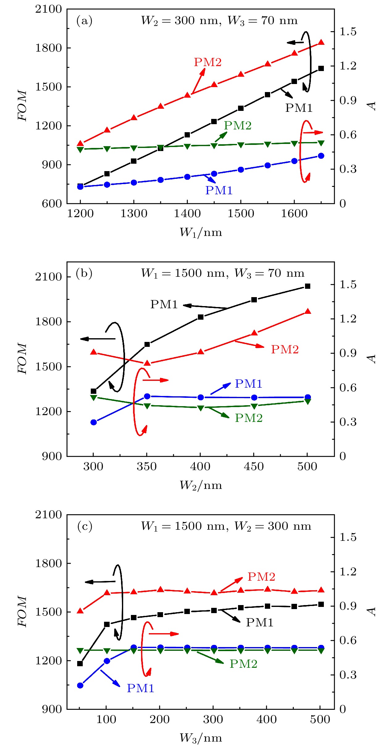
图 4 PM 1和PM 2 的FOM 和A随(a)W1 (= H1), (b) W2 (= H2)和(c) W3 (= H3)变化的规律, W1 (= H1), W2 (= H2) 和W3 (= H3)分别取1500 nm, 300 nm和70 nm
Figure 4. FOM and A of the PM 1 and PM 2 with different: (a) W1 (= H1) at W2 (= H2) = 300 nm and W3 (= H3) = 70 nm; (b) W2(= H2) at W1 (= H1) = 1500 nm and W3 (= H3) = 70 nm; (c) W3 (= H3) at W2 (= H2) = 300 nm and W1 (= H1) = 1500 nm.
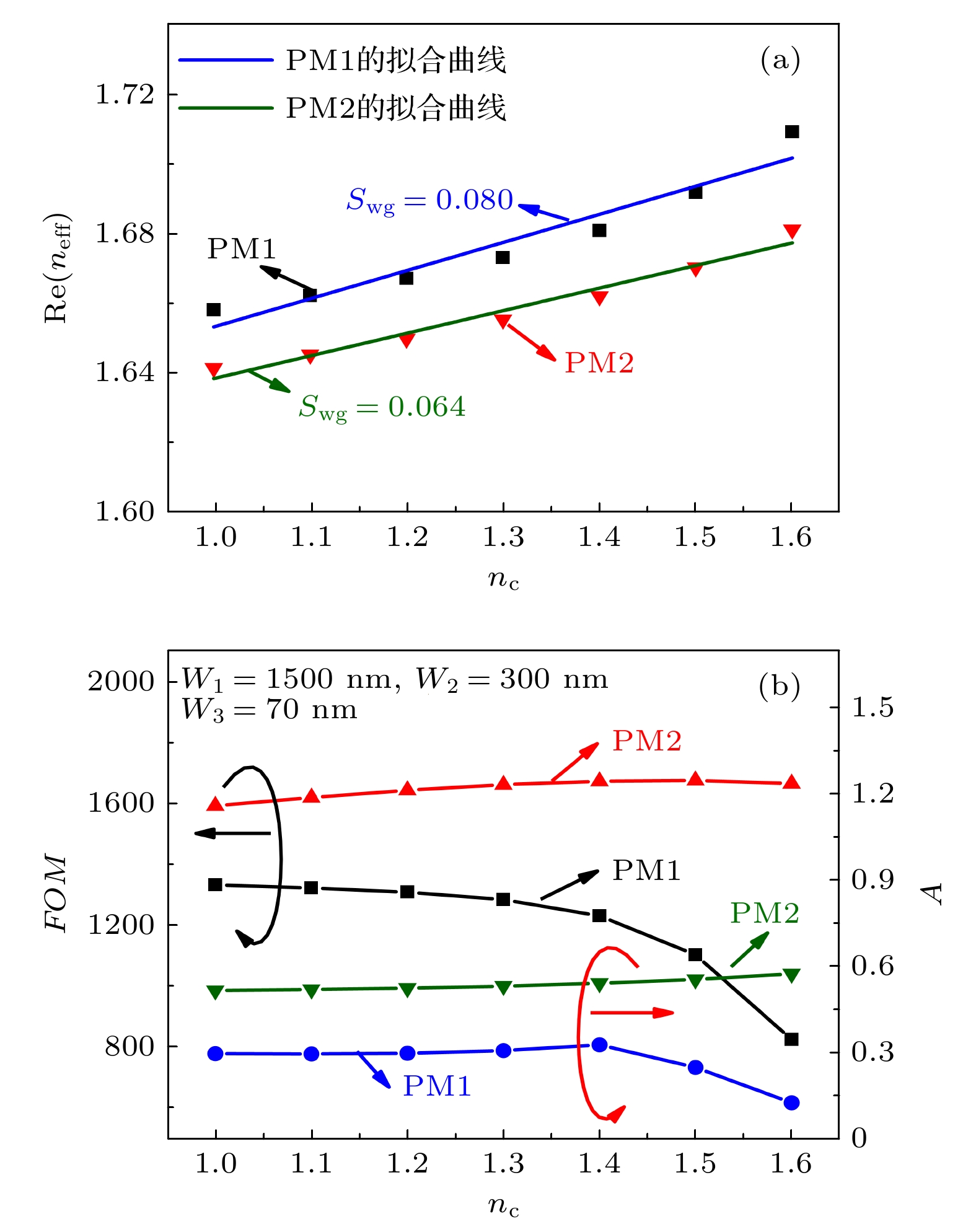
图 5 在不同的nc下, PM 1和PM 2的(a) Re(neff), (b) FOM和A的变化规律, W1 (= H1), W2 (= H2) 和W3 (= H3)分别取1500 nm, 300 nm和70 nm
Figure 5. (a) Re(neff) and (b) FOM and A of the PM 1 and PM 2 with different nc as W1 (= H1) = 1500 nm, W2 (= H2) = 300 nm and W3 (= H3) = 70 nm.
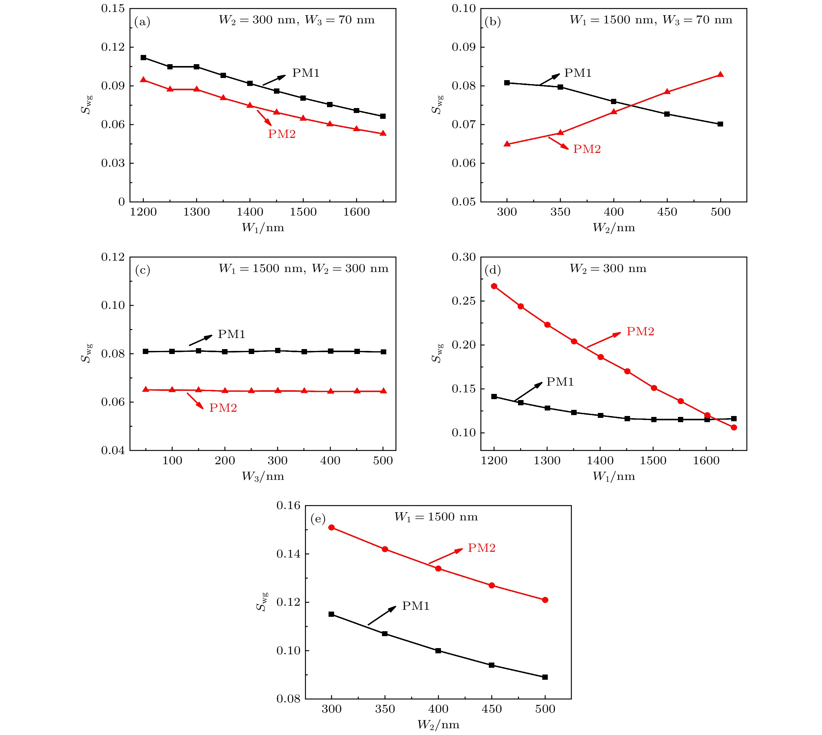
图 6 非对称PS-CaF2混合等离子体波导的PM 1 和 PM 2 的Swg 随(a) W1 (= H1), (b) W2 (= H2)和(c) W3 (= H3) 的变化规律, W1 (= H1), W2 (= H2) 和W3 (= H3)分别取1500 nm, 300 nm和70 nm; 无Ag膜波导的PM 1 和 PM 2 的Swg 随(d) W1 (= H1)和 (e) W2 (= H2)的变化规律, W1(= H1)和W2(= H2)分别取1500 nm和300 nm
Figure 6. with an asymmetric Ag film of Swg of the PM 1 and PM 2 in the PS-CaF2HPW with an asymmetric Ag films with different: (a) W1 (= H1) at W2 (= H2) = 300 nm and W3 (= H3) = 70 nm; (b) W2 (= H2) at W1 (= H1) = 1500 nm and W3 (= H3) = 70 nm; (c) W3 (= H3) at W2 (= H2) = 300 nm and W1 (= H1) = 1500 nm. Without an asymmetric Ag film of Swg of the PM 1 and PM 2 in the waveguide without an asymmetric Ag film of with different (d) W1 (= H1) at W2 (= H2) = 300 nm; (b) W2 (= H2) at W1 (= H1) = 1500 nm.
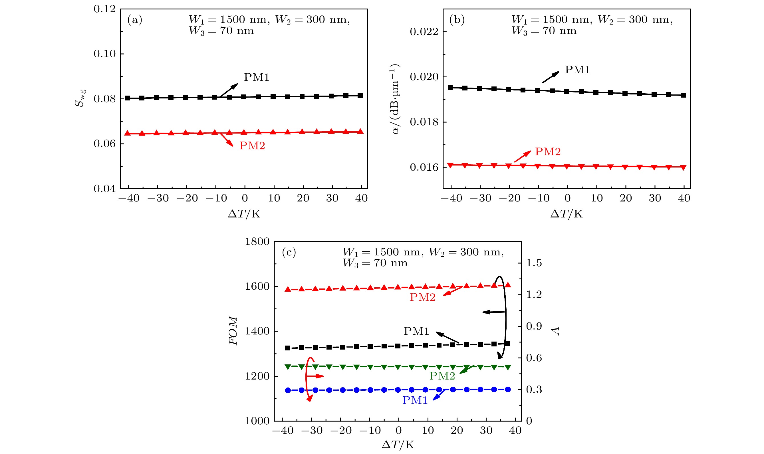
图 7 W1 (= H1) = 1500 nm, W2 (= H2) = 300 nm和W3 (= H3) = 70 nm时, 在不同的ΔT下 (a) Re(neff), (b) α, (c) FOM和A的变化规律
Figure 7. (a) Re(neff), (b) α, (c) FOM and A with different ΔT as W1 (= H1) = 1500 nm, W2 (= H2) = 300 nm and W3 (= H3) = 70 nm
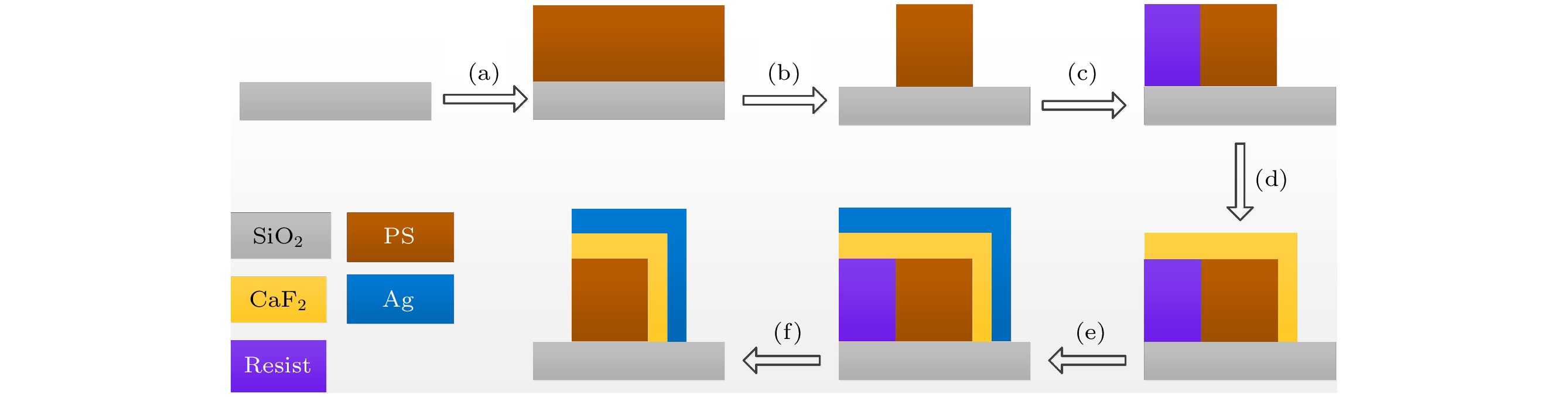
图 8 制造流程 (a)在SiO2衬底上外延生长PS层; (b)电子束光刻使其成型; (c)涂上抗蚀剂; (d) 在PS上外延生长CaF2层; (e) 倾斜沉积金属Ag层; (f)电子束光刻使其成型, 并清除抗蚀剂
Figure 8. (a) Grow PS on a SiO2 substrate; (b) pattern the resist through E-beam lithography; (c) it is coated with a resist; (d) grow CaF2 layers epitaxially on a PS layer; (e) oblique deposition of metal Ag; (f) electron beam lithography moulds it and removes the resist.
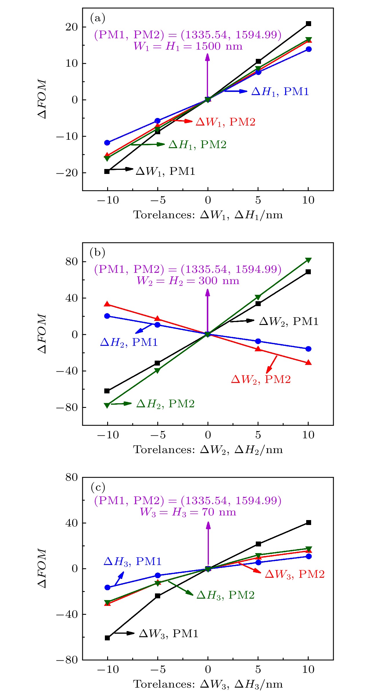
图 9 不同的尺寸容差下, PM 1和PM 2 的FOM的变化 (ΔFOM)随(a) ΔW1和ΔH, (b) ΔW2和ΔH2; (c) ΔW3和ΔH3的变化规律, W1 (= H1), W2 (= H2) 和W3 (= H3)分别取1500 nm, 300 nm和70 nm
Figure 9. The changes of FOM (ΔFOM
) for the PM 1 and PM 2 with different dimensional tolerances: (a) ΔW1 and ΔH1 at W2 (= H2) = 300 nm and W3 (= H3) = 70 nm; (b) ΔW2 and ΔH2 at W1 (= H1) = 1500 nm and W3 (= H3) = 70 nm; (c) ΔW3 and ΔH3 at W1 (= H1) = 1500 nm and W2 (= H2) = 300 nm. 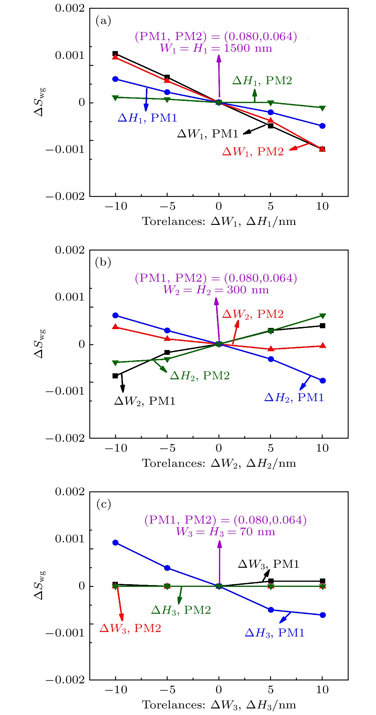
图 11 不同的尺寸容差, PM 1和PM 2 的Swg (ΔSwg)随(a) ΔW1和ΔH1, (b) ΔW2和ΔH2, (c) ΔW3和ΔH3的变化规律. W1(= H1), W2(= H2) 和W3(= H3)分别取1500 nm, 300 nm和70 nm
Figure 11. The changes of Swg (ΔSwg) for the PM 1 and PM 2 with different dimensional tolerances: (a) ΔW1 and ΔH1 at W2(= H2) = 300 nm and W3(= H3) = 70 nm; (b) ΔW2 and ΔH2 at W1(= H1) = 1500 nm and W3(= H3) = 70 nm; (c) ΔW3 and ΔH3 at W1(= H1) = 1500 nm and W2(= H2) = 300 nm.
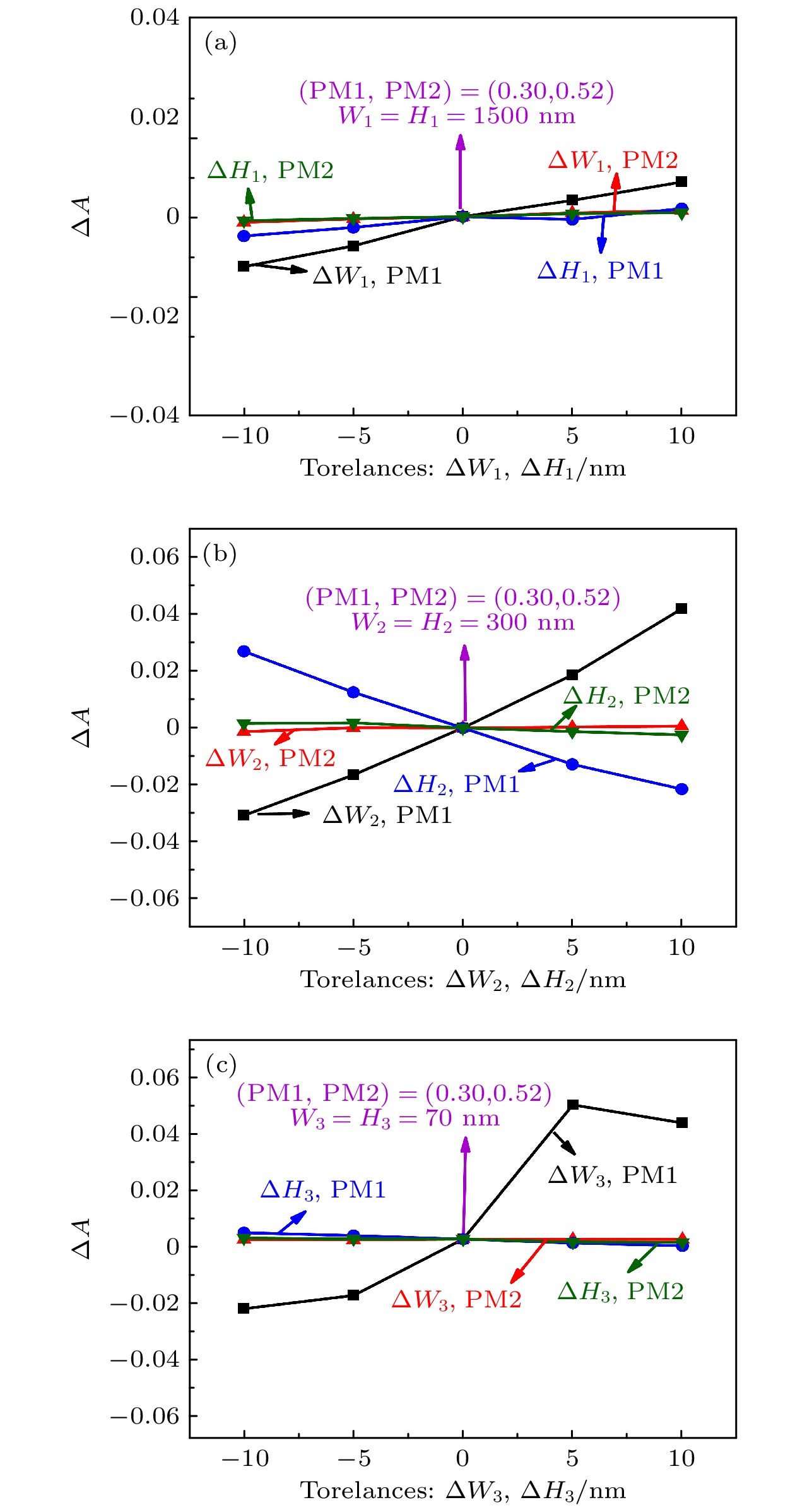
图 10 在不同的尺寸容差下, PM 1和PM 2 的A 的变化(ΔA)随(a) ΔW1和ΔH1, (b) ΔW2和ΔH2, (c) ΔW3和ΔH3的变化规律. W1(= H1), W2(= H2) 和W3(= H3)分别取1500 nm, 300 nm和70 nm
Figure 10. The changes of A (ΔA) for the PM 1 and PM 2 with different dimensional tolerances: (a) ΔW1 and ΔH1 at W2 (= H2) = 300 nm and W3 (= H3) = 70 nm; (b) ΔW2 and ΔH2 at W1 (= H1) = 1500 nm and W3 (= H3) = 70 nm; and (c) ΔW3 and ΔH3 at W1 (= H1) = 1500 nm and W2 (= H2) = 300 nm.
-
[1] Oulton R F, Sorger V J, Genov D A, Pile D F P, Zhang X 2008 Nat. Photonics 2 496
Google Scholar
[2] Burstein E, Chen W P, Chen Y J, Hartstein A 1974 J. Vac. Sci. Technol. 11 1004
Google Scholar
[3] Garcia de Abajo F J, Saenz J J 2005 Phys. Rev. Lett. 95 233901
Google Scholar
[4] Yang L K, Li P, Wang H C, Li Z P 2018 Chin. Phys. B. 27 094216
Google Scholar
[5] Zhang H F, Cao D, Tao F, Yang X H, Wang Y, Yan X N, Bai L H 2010 Chin. Phys. B. 19 027301
Google Scholar
[6] Gong P Q, Li X G, Zhou X, Zhang Y A, Chen N, Wang S K, Zhang S Q, Zhao Y 2021 Opt. Laser Technol. 139 106981
Google Scholar
[7] Smith C L, Thilsted A H, Garcia-Ortiz C E, Radko I P, Marie R, Jeppesen C, Vannahme C, Bozhevolnyi S I, Kristensen A 2014 Nano Lett. 14 1659
Google Scholar
[8] Kumari B, Barh A, Varshney R K, Pal B P 2016 Sens. Actuators, B 236 759
Google Scholar
[9] Kumari B, Varshney R K, Pal B P 2018 Sens. Actuators, B 255 3409
Google Scholar
[10] Mortensen N A, Bozhevolnyi S I, Alù A 2019 Nanophotonics 8 1315
Google Scholar
[11] Nedeljkovic M, Stankovic S, Mitchell C J, Khokhar A Z, Reynolds S A, Thomson D J, Gardes F Y, Littlejohns C G, Reed G T, Mashanovich G Z 2014 IEEE Photonics Technol. Lett. 26 1352
Google Scholar
[12] Shen L, Healy N, Mitchell C J, Penades J S, Nedeljkovic M, Mashanovich G Z, Peacock A C 2015 Opt. Lett. 40 268
Google Scholar
[13] Cheng Z Z, Chen X, Wong C Y, Xu K, Tsang H K 2012 IEEE Photonics J. 4 1510
Google Scholar
[14] Shankar R, Bulu I, Lončar M 2013 Appl. Phys. Lett. 102 051108
Google Scholar
[15] El Shamy R S, Swillam M A, Khalil D A 2019 J. Lightwave Technol. 37 4394
Google Scholar
[16] Alonso-Ramos C, Nedeljkovic M, Benedikovic D, Penades J S, Littlejohns C G, Khokhar A Z, Perez-Galacho D, Vivien L, Cheben P, Mashanovich G Z 2016 Opt. Lett. 41 4324
Google Scholar
[17] Hassan K, Leroy F, Colas-des-Francs G, Weeber J C 2014 Opt. Lett. 39 697
Google Scholar
[18] Dai D X, He S L 2009 Opt. Express 17 16646
Google Scholar
[19] Mai W J, Wang Y L, Zhang Y Y, Cui L N, Yu L 2017 Chin. Phys. B. 34 024204
Google Scholar
[20] 王志斌, 尹少杰, 段晓宁, 邓玉萍, 董伟, 孔祥瑞 2020 中国激光 47 0313001
Google Scholar
Wang Z B, Yin S J, Duan X N, Deng Y P, Dong W, Kong X R 2020 Chin. J. Las. 47 0313001
Google Scholar
[21] Heo J H, Shin D H, Kim S, Jang M H, Lee M H, Seo S W, Choi S H, Im S H 2017 J. Chem. Eng. Jpn. 323 153
Google Scholar
[22] Hwang K W, Park S H 2015 Mater. Res. Innovations 19 S8
Google Scholar
[23] Chen F, Lv H, Pang Z, Zhang J, Hou Y, Gu Y, Yang H, Yang G 2019 IEEE Sens. J. 19 8441
Google Scholar
[24] Olenych I B, Monastyrskii L S, Aksimentyeva O I, Orovcík L, Salamakha M Y 2019 Mol. Cryst. Liq. Cryst. 673 32
Google Scholar
[25] 孙鹏, 胡明, 刘博, 孙凤云, 许路加 2011 物理学报 60 057303
Google Scholar
Sun P, Hu M, Liu B, Sun F Y, Xun L J 2011 Acta. Phys. Sin. 60 057303
Google Scholar
[26] 陈颖, 范卉青, 卢波 2014 物理学报 63 244207
Google Scholar
Chen Y, Fan H Q, Lu B 2014 Acta. Phys. Sin. 63 244207
Google Scholar
[27] Chan K C, Tso C Y, Hussain A, Chao C Y H 2019 Appl. Therm. Eng. 161 114112
Google Scholar
[28] Gan F L, Wang B D, Jin Z H, Xie L L, Dai Z D, Zhou T X, Jiang X 2021 Sci. Total. Environ. 768 144529
Google Scholar
[29] Girault P, Azuelos P, Lorrain N, Poffo L, Lemaitre J, Pirasteh P, Hardy I, Thual M, Guendouz M, Charrier J 2017 Opt. Mater. 72 596
Google Scholar
[30] Palik E D 1985 Academic Press 39 1
[31] Ciminelli C, Campanella C M, Dell’Olio F, Campanella C E, Armenise M N 2013 Prog. Quantum Electron. 37 51
Google Scholar

 DownLoad:
Catalog
Metrics
- Abstract views: 3638
- PDF Downloads: 77
- Cited By: 0
