


-
Cd3As2, especially its various nanostructures, has been considered as an excellent candidate for application in novel optoelectronic devices due to its ultrahigh mobility and good air-stability. Recent researches exhibited Cd3As2 as a candidate of thermoelectric materials by virtue of its ultralow thermal conductivity in comparison with other semimetals or metals. In this work, at first ( Cd1–xMnx)3As2 (x = 0, 0.05, 0.1) bulk alloys are prepared by high-pressure sintering to suppress the volatilization of As element, and then several kinds of Mn3As2-doped Cd3As2 nanostructures are obtained on mica substrates by chemical vapor deposition (CVD), with bamboo-shoot-nanowire structure forming in a high-temperature region and films in a low-temperature region. Effects of Mn3As2 doping on the crystalline structure, phase compositions, microstructures and thermoelectric properties of the Cd3As2 nanostructures are systematically studied. Energy-dispersive spectrometer (EDS) analysis at various typical positions of the Mn3As2-doped Cd3As2 nanostructures shows that the Mn content in these nanostructures is in a range of 0.02%–0.18% (atomic percent), which is much lower than the Mn content in ( Cd1–xMnx)3As2 (x = 0, 0.05, 0.1) parent alloys. The main phases of these nanostructures are all body centered tetragonal α phase with a small amount of primitive tetragonal α′ phase. Doping results in the α″ phase and Mn2As impurity phase occurring. The Cd3As2 film presents a self-assembled cauliflower microstructure. Upon Mn3As2 doping, this morphology finally transforms into a vertical-growth seashell structure. In a high temperature region of the mica substrate, a unique bamboo-shoot-nanowire structure is formed, with vertical-growth bamboo shoots connected by nanowires, and at the end of these nanowires grows a white pentagonal flower structure with the highest Mn content of 0.18% (atomic percent) for all the nanostructures. Conductivity of the Cd3As2 film and the bamboo-shoot-nanowire structure are ~20 and 320 S/cm, respectively. The remarkable conductivity enhancement can be attributed to higher crystallinity and the formation of nanowire conductive network, which significantly increase carrier concentration and Hall mobility. The Hall mobility values of the nanowire structures range from 2271 to 3048 cm2/(V·s) much higher than the values of 378–450 cm2/(V·s) for the films. The Seebeck coefficient for the bamboo-shoot-nanowire structure is in a range of 59–68 µV/K, which is about 15% higher than those for the films (50–61 µV/K). Although maximal power factor of the bamboo-shoot-nanowire structure is 14 times as high as that of the thin film, reaching 0.144 mW/(m·K2) at room temperature, this value is still one order of magnitude lower than the previously reported value of 1.58 mW/(m·K2) for Cd3As2 single crystal.
-
Keywords:
- thermoelectric properties /
- Cd3As2 /
- chemical vapor deposition /
- nanostructure
[1] Kaleem U, Meng Y F, Sun Y, et al. 2020 Appl. Phys. Lett. 117 011102
 Google Scholar
[2] Wang H L, Ma J L, Wei Q Q, Zhao J H 2020 J. Semicond. 41 072903
Google Scholar
[3] Zhang Y X, Nappini S, Sankar R, Bondino F, Gao J F, Politano A 2021 J. Mater. Chem. C 9 1235
Google Scholar
[4] Liang T, Gibson Q, Ali M N, Liu M H, Cava R J, Ong N P 2015 Nat. Mater. 14 280
Google Scholar
[5] Cheng P H, Zhang C, Liu Y W, et al. 2016 New J. Phys. 18 083003
Google Scholar
[6] Park K, Jung M, Kim D, Bayogan J R, Lee J H, An S J, Seo J, Seo J, Ahn J P, Park J 2020 Nano Lett. 20 4939
Google Scholar
[7] Suslov A V, Davydov A B, Oveshnikov L N, et al. 2019 Phys. Rev. B 99 094512
Google Scholar
[8] Zhou T, Zhang C, Zhang H S, Xiu F X, Yang Z Q 2016 Inorg. Chem. Front. 3 1637
Google Scholar
[9] Zhang C, Zhou T, Liang S H, et al. 2016 Chin. Phys. B 25 017202
Google Scholar
[10] Wang H H, Luo X G, Peng K L, et al. 2019 Adv. Funct. Mater. 29 1902437
Google Scholar
[11] Pariari A, Khan N, Singha R, Satpati B, Mandal P 2016 Phys. Rev. B 94 165139
Google Scholar
[12] 杨亮亮, 勤源浩, 魏江涛, 宋培帅, 张明亮, 杨富华, 王晓东 2021 物理学报 70 076802
Google Scholar
Yang L L, Qin Y H, Wei J T, Song P S, Zhang M L, Yang F H, Wang X D 2021 Acta Phys. Sin. 70 076802
Google Scholar
[13] 李彩云, 何文科, 王东洋, 张潇, 赵立东 2021 物理学报 70 208401
Google Scholar
Li C Y, He W K, Wang D Y, Zhang X, Zhao L D 2021 Acta Phys. Sin. 70 208401
Google Scholar
[14] Sun N K, Li W, Pang C, Zhong D H, Li M L 2021 Solid State Commun. 339 114505
Google Scholar
[15] Liao W W, Yang L, Chen J, et al. 2019 Chem. Eng. J. 371 593
Google Scholar
[16] Yue Z M, Zhao K P, Chen H Y, Qiu P F, Zhao L D, Shi X 2021 Chin. Phys. Lett. 38 117201
Google Scholar
[17] 胡威威, 孙进昌, 张玗, 龚悦, 范玉婷, 唐新峰, 谭刚健 2022 物理学报 71 047101
Google Scholar
Hu W W, Sun J C, Zhang Y, Guo Y, Fan Y T, Tang X F, Tan G J 2022 Acta Phys. Sin. 71 047101
Google Scholar
[18] Chen R K, Lee J, Lee W, Li D Y 2019 Chem. Rev. 119 9260
Google Scholar
[19] Zhu G P, Zhao C W, Wang X W, Wang J 2021 Chin. Phys. Lett. 38 024401
Google Scholar
[20] Guo J, Zhao X G, Sun N K, Xiao X F, Liu W, Zhang Z D 2021 J. Mater. Sci. Technol. 76 247
Google Scholar
[21] Celinski Z, Burian A, Rzepa B, Zdanowicz W 1987 Mat. Res. Bull. 22 419
Google Scholar
[22] Ril A I, Marenkin S F, Volkov V V, Oveshnikov L N, Kozlov V V 2021 J. Alloys Compd. 892 162082
[23] Oveshnikov L N, Davydov A B, Suslov A V, Ril A I, Marenkin S F, Vasiliev A L, Aronzon B A 2020 Sci. Rep. 10 4601
Google Scholar
[24] Wei S, Lu J, Yu W C, Zhang H B, Qian Y T 2006 Cryst. Growth Des. 6 849
Google Scholar
[25] Weszka J 1999 Phys. Stat. Sol. (b) 211 605
Google Scholar
[26] Davydov A B, Oveshnikov L N, SuSlov A V, Ril A I, Marenkin S F, Aronzon B A 2020 Phys. Solid State 62 419
Google Scholar
[27] Marenkin S F, Trukhan V M, Fedorchenko I V, TruKhanov S V, Shoukavaya T V 2014 Russ. J. Inorg. Chem. 59 355
Google Scholar
[28] Li C Z, Zhu R, Ke X X, Zhang J M, Wang L X, Zhang L, Liao Z M, Yu D P 2015 Cryst. Growth Des. 15 3264
Google Scholar
[29] Rice A D, Park K, Hughes E T, Mukherjee K, Alberi K 2019 Phys. Rev. Mater. 3 121201
Google Scholar
[30] Li C Z, Wang L X, Liu H W, Wang J, Liao Z M, Yu D P 2015 Nat. Commun. 6 10137
Google Scholar
[31] Schonherr P, Hesjedal T 2015 Appl. Phys. Lett. 106 013115
Google Scholar
[32] Hwang Y, Choi J, Dung D D, Shin Y, Cho S 2011 J. Appl. Phys. 109 063914
Google Scholar
[33] Dai Z J, Manjappa M, Yang Y K, Tan T C W, Qiang B, Han S, Wong L J, Xiu F X, Liu W W, Singh R 2021 Adv. Funct. Mater. 31 2011011
Google Scholar
[34] Nishihaya S, Uchida M, Nakazawa Y, Akiba K, Kriener M, Kozuka Y, Miyake A, Taguchi Y, Tokunaga M, Kawasaki M 2018 Phys. Rev. B 97 245103
Google Scholar
[35] Jia Z Z, Li C Z, Li X Q, Shi J R, Liao Z M, Yu D P, Wu X S 2016 Nat. Commun. 7 13013
Google Scholar
-

图 1 Mn3As2掺杂Cd3As2纳米结构制备流程示意图
Figure 1. Schematic diagram of preparation process of Mn3As2-doped Cd3As2 nanostructures.

图 2 Mn3As2掺杂Cd3As2薄膜、竹笋纳米线结构的XRD, 以及3种Cd3As2晶体结构标准卡片图
Figure 2. XRD patterns of Mn3As2-doped Cd3As2 films and bamboo-shoot-nanowire structures and standard XRD cards of three Cd3As2 crystalline structures.
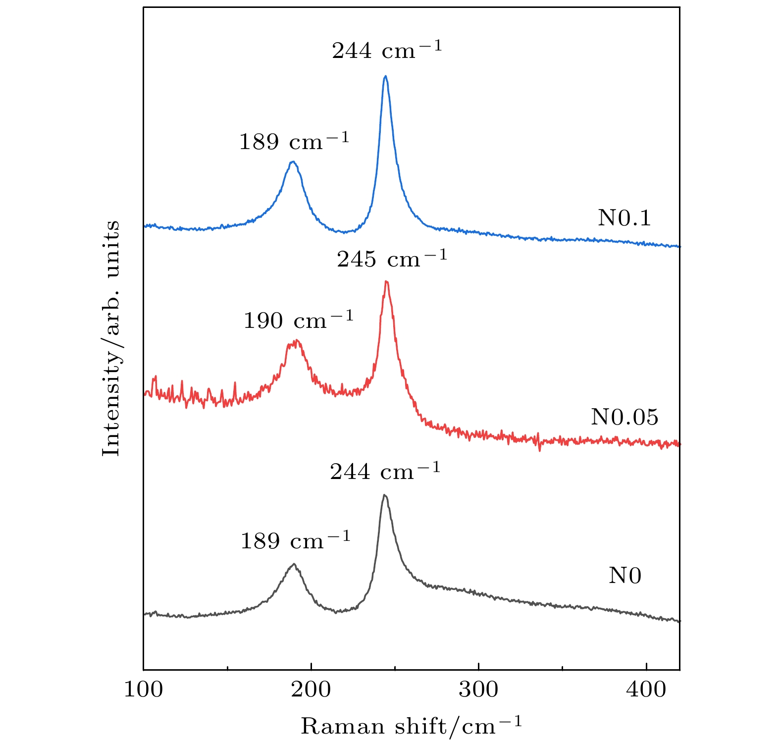
图 3 Mn3As2掺杂Cd3As2竹笋纳米线结构的拉曼光谱图
Figure 3. Laman spectra of Mn3As2-doped bamboo-shoot-nanowire structures.
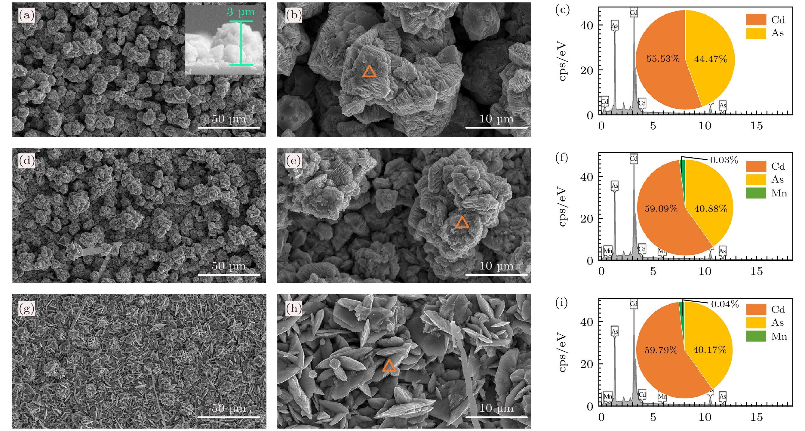
图 4 Mn3As2掺杂Cd3As2薄膜的SEM图(第1和第2列)及EDS分析结果(第3列) (a)—(c) F0样品 ((a)插图为薄膜横截面图); (d)—(f) F0.05样品; (g)—(i) F0.1样品
Figure 4. SEM images (the first and second column) and EDS analysis results (the third column) of Mn3As2-doped Cd3As2 films: (a)–(c) F0 sample (the inset of (a) shows the fracture morphology); (d)–(f) F0.05 sample; (g)–(i) F0.1 sample.

图 5 Mn3As2掺杂Cd3As2纳米线的SEM (第1和第2列)及EDS分析结果(第3和第4列) (a)—(d) N0 样品; (e)—(h) N0.05 样品; (i)—(l) N0.1样品
Figure 5. SEM images (the first and second column) and EDS analysis results (the third and fourth column) of Mn3As2-doped Cd3As2 nanowires: (a)–(d) N0 sample; (e)–(h) N0.05 sample; (i)–(l) N0.1 sample.

图 6 Cd3As2竹笋纳米线结构横截面的SEM图(a)—(c)及EDS元素成分分析结果(d), (e)
Figure 6. SEM images of the fracture cross section (a)–(c) and EDS analysis and compositional distributions (d), (e) of Cd3As2 bamboo-shoot-nanowire structure.

图 7 Cd3As2纳米线的微结构表征 (a) TEM图; (b) 元素成分; (c) HRTEM图; (d) 电子衍射花样图
Figure 7. Microstructure characteristics of Cd3As2 nanowires: (a) TEM image; (b) elemental compositions; (c) HRTEM image; (d) selected area electron diffraction image.

图 8 (a)—(c) Mn3As2掺杂Cd3As2薄膜的电导率 (a)、塞贝克系数(b)、功率因子(c)随温度的变化曲线; (d) Mn3As2掺杂Cd3As2薄膜的室温载流子浓度和霍尔迁移率
Figure 8. (a)–(c) Temperature dependence of electrical conductivity (a), Seebeck coefficient (b), and power factor (c) of Mn3As2-doped Cd3As2 films; (d) room-temperature carrier concentration and Hall mobility (d) of Mn3As2-doped Cd3As2 films.

图 9 (a)—(c) Mn3As2掺杂Cd3As2竹笋纳米线结构的电导率 (a)、塞贝克系数 (b)、功率因子(c)随温度的变化曲线; (d) Mn3As2掺杂Cd3As2竹笋纳米线结构的室温载流子浓度和霍尔迁移率
Figure 9. (a)–(c) Temperature dependence of electrical conductivity (a), Seebeck coefficient (b), and power factor (c) of Mn3As2-doped Cd3As2 bamboo-shoot-nanowire structure; (d) room-temperature carrier concentration and Hall mobility of Mn3As2-doped Cd3As2 bamboo-shoot-nanowire structure.
-
[1] Kaleem U, Meng Y F, Sun Y, et al. 2020 Appl. Phys. Lett. 117 011102
Google Scholar
[2] Wang H L, Ma J L, Wei Q Q, Zhao J H 2020 J. Semicond. 41 072903
Google Scholar
[3] Zhang Y X, Nappini S, Sankar R, Bondino F, Gao J F, Politano A 2021 J. Mater. Chem. C 9 1235
Google Scholar
[4] Liang T, Gibson Q, Ali M N, Liu M H, Cava R J, Ong N P 2015 Nat. Mater. 14 280
Google Scholar
[5] Cheng P H, Zhang C, Liu Y W, et al. 2016 New J. Phys. 18 083003
Google Scholar
[6] Park K, Jung M, Kim D, Bayogan J R, Lee J H, An S J, Seo J, Seo J, Ahn J P, Park J 2020 Nano Lett. 20 4939
Google Scholar
[7] Suslov A V, Davydov A B, Oveshnikov L N, et al. 2019 Phys. Rev. B 99 094512
Google Scholar
[8] Zhou T, Zhang C, Zhang H S, Xiu F X, Yang Z Q 2016 Inorg. Chem. Front. 3 1637
Google Scholar
[9] Zhang C, Zhou T, Liang S H, et al. 2016 Chin. Phys. B 25 017202
Google Scholar
[10] Wang H H, Luo X G, Peng K L, et al. 2019 Adv. Funct. Mater. 29 1902437
Google Scholar
[11] Pariari A, Khan N, Singha R, Satpati B, Mandal P 2016 Phys. Rev. B 94 165139
Google Scholar
[12] 杨亮亮, 勤源浩, 魏江涛, 宋培帅, 张明亮, 杨富华, 王晓东 2021 物理学报 70 076802
Google Scholar
Yang L L, Qin Y H, Wei J T, Song P S, Zhang M L, Yang F H, Wang X D 2021 Acta Phys. Sin. 70 076802
Google Scholar
[13] 李彩云, 何文科, 王东洋, 张潇, 赵立东 2021 物理学报 70 208401
Google Scholar
Li C Y, He W K, Wang D Y, Zhang X, Zhao L D 2021 Acta Phys. Sin. 70 208401
Google Scholar
[14] Sun N K, Li W, Pang C, Zhong D H, Li M L 2021 Solid State Commun. 339 114505
Google Scholar
[15] Liao W W, Yang L, Chen J, et al. 2019 Chem. Eng. J. 371 593
Google Scholar
[16] Yue Z M, Zhao K P, Chen H Y, Qiu P F, Zhao L D, Shi X 2021 Chin. Phys. Lett. 38 117201
Google Scholar
[17] 胡威威, 孙进昌, 张玗, 龚悦, 范玉婷, 唐新峰, 谭刚健 2022 物理学报 71 047101
Google Scholar
Hu W W, Sun J C, Zhang Y, Guo Y, Fan Y T, Tang X F, Tan G J 2022 Acta Phys. Sin. 71 047101
Google Scholar
[18] Chen R K, Lee J, Lee W, Li D Y 2019 Chem. Rev. 119 9260
Google Scholar
[19] Zhu G P, Zhao C W, Wang X W, Wang J 2021 Chin. Phys. Lett. 38 024401
Google Scholar
[20] Guo J, Zhao X G, Sun N K, Xiao X F, Liu W, Zhang Z D 2021 J. Mater. Sci. Technol. 76 247
Google Scholar
[21] Celinski Z, Burian A, Rzepa B, Zdanowicz W 1987 Mat. Res. Bull. 22 419
Google Scholar
[22] Ril A I, Marenkin S F, Volkov V V, Oveshnikov L N, Kozlov V V 2021 J. Alloys Compd. 892 162082
[23] Oveshnikov L N, Davydov A B, Suslov A V, Ril A I, Marenkin S F, Vasiliev A L, Aronzon B A 2020 Sci. Rep. 10 4601
Google Scholar
[24] Wei S, Lu J, Yu W C, Zhang H B, Qian Y T 2006 Cryst. Growth Des. 6 849
Google Scholar
[25] Weszka J 1999 Phys. Stat. Sol. (b) 211 605
Google Scholar
[26] Davydov A B, Oveshnikov L N, SuSlov A V, Ril A I, Marenkin S F, Aronzon B A 2020 Phys. Solid State 62 419
Google Scholar
[27] Marenkin S F, Trukhan V M, Fedorchenko I V, TruKhanov S V, Shoukavaya T V 2014 Russ. J. Inorg. Chem. 59 355
Google Scholar
[28] Li C Z, Zhu R, Ke X X, Zhang J M, Wang L X, Zhang L, Liao Z M, Yu D P 2015 Cryst. Growth Des. 15 3264
Google Scholar
[29] Rice A D, Park K, Hughes E T, Mukherjee K, Alberi K 2019 Phys. Rev. Mater. 3 121201
Google Scholar
[30] Li C Z, Wang L X, Liu H W, Wang J, Liao Z M, Yu D P 2015 Nat. Commun. 6 10137
Google Scholar
[31] Schonherr P, Hesjedal T 2015 Appl. Phys. Lett. 106 013115
Google Scholar
[32] Hwang Y, Choi J, Dung D D, Shin Y, Cho S 2011 J. Appl. Phys. 109 063914
Google Scholar
[33] Dai Z J, Manjappa M, Yang Y K, Tan T C W, Qiang B, Han S, Wong L J, Xiu F X, Liu W W, Singh R 2021 Adv. Funct. Mater. 31 2011011
Google Scholar
[34] Nishihaya S, Uchida M, Nakazawa Y, Akiba K, Kriener M, Kozuka Y, Miyake A, Taguchi Y, Tokunaga M, Kawasaki M 2018 Phys. Rev. B 97 245103
Google Scholar
[35] Jia Z Z, Li C Z, Li X Q, Shi J R, Liao Z M, Yu D P, Wu X S 2016 Nat. Commun. 7 13013
Google Scholar

 DownLoad:
Catalog
Metrics
- Abstract views: 2755
- PDF Downloads: 36
- Cited By: 0
