


-
With the shrink of critical dimensions of semiconductor devices to a few nanometers, atomic layer etching (ALE) has become an important technique to achieve single-atom resolution. The ALE can divide plasma etching into two self-limiting reaction processes: passivation process and etching process, allowing for the sequential removal of material atomic layer by layer. Therefore, it encounters the problem of low etch rate. In this work, the variation in surface substance coverage during the passivation process and the etching process are investigated numerically to optimize both the passivation duration and the etching duration. A coupled model integrating a two-dimensional inductively coupled plasma discharge chamber model, a one-dimensional sheath model, and a three-dimensional etching trench model is developed and used to investigate the optimal time for one single cycle ALE of silicon through the use of Ar/Cl2 gases under the condition of Ar inductively coupled plasma discharge. The results indicate that during the passivation stage, the surface coverage of SiCl and SiCl2 initially increase with time going by and then decrease, while the surface coverage of SiCl3 continuously increases, and eventually, the surface coverage of these three species stabilize. When the surface is predominantly covered by SiCl2, it is the optimal time to trigger the etching process, which induces a relatively favorable surface state and a relatively short etching time. Comparing with typical ALE etching techniques, the time of our optimal ALE single cycle is shortened by about 33.89%. The ALE cycle time (etching rate) exhibits a linear relationship with the aspect ratio. Additionally, the duration of the passivation process and etching process increase linearly with the aspect ratio or etch depth increasing. Moreover, as the etch depth increases, the effect of the passivation process on the ALE rate becomes more significant than that of the etching process.
-
Keywords:
- atomic layer etching /
- passivation and etching time /
- the component of passivated layer /
- aspect ratio
[1] Jung J, Kim K 2023 Materials 16 3611
 Google Scholar
[2] Hao Q, Kim P, Nam S K, Kang S Y, Donnelly V M 2023 J. Vac. Sci. Technol., A 41 032605
Google Scholar
[3] Eliceiri M, Rho Y, Li R, Grigoropoulos C P 2023 J. Vac. Sci. Technol., A 41 022602
Google Scholar
[4] Ma X, Zhang S, Dai Z, Wang Y 2017 Plasma Sci. Technol. 19 085502
Google Scholar
[5] Huard C M, Zhang Y, Sriraman S, Paterson A, Kanarik K J, Kushner M J 2017 J. Vac. Sci. Technol., A 35 031306
Google Scholar
[6] Horiike Y, Tanaka T, Nakano M, Iseda S, Sakaue H, Nagata A, Shindo H, Miyazaki S, Hirose M 1990 J. Vac. Sci. Technol. , A 8 1844
Google Scholar
[7] Matsuura T, Murota J, Sawada Y, Ohmi T 1993 Appl. Phys. Lett. 63 2803
Google Scholar
[8] Imai S, Haga T, Matsuzaki O, Hattori T, Matsumura M 1995 Jpn. J. Appl. Phys., Part 1 34 5049
Google Scholar
[9] Kim J K, Cho S I, Lee S H, Kim C K, Min K S, Kang S H, Yeom G Y 2013 J. Vac. Sci. Technol., A 31 061310
Google Scholar
[10] Song E J, Kim J H, Kwon J D, Kwon S H, Ahn J H 2018 Jpn. J. Appl. Phys. 57 106505
Google Scholar
[11] Goodyear A, Cooke M 2017 J. Vac. Sci. Technol., A 35 01A105
Google Scholar
[12] Yoon M Y, Yeom H J, Kim J H, Chegal W, Cho Y J, Kwon D C, Jeong J R, Lee H C 2021 Phys. Plasmas 28 063504
Google Scholar
[13] Nakamura S, Tanide A, Kimura T, Nadahara S, Ishikawa K, Oda O, Hori M 2023 J. Appl. Phys. 133 043302
Google Scholar
[14] Ranjan A, Wang M, Sherpa S D, Rastogi V, Koshiishi A, Ventzek P L G 2016 J. Vac. Sci. Technol., A 34 031304
Google Scholar
[15] Agarwal A, Kushner M J 2009 J. Vac. Sci. Technol., A 27 37
Google Scholar
[16] Huard C M, Lanham S J, Kushner M J 2018 J. Phys. D: Appl. Phys. 51 155201
Google Scholar
[17] 贺平逆, 宁建平, 秦尤敏, 赵成利, 苟富均 2011 物理学报 60 045209
Google Scholar
He P N, Ning J P, Qin Y M, Zhao C L, Gou F J 2011 Acta Phys. 60 045209
Google Scholar
[18] Vella J R, Humbird D, Graves D B 2022 J. Vac. Sci. Technol., B 40 023205
Google Scholar
[19] Sui J, Zhang S, Liu Z, Yan J, Dai Z 2016 Plasma Sci. Technol. 18 666
Google Scholar
[20] 葛婕 2014 硕士学位论文 (北京: 清华大学)
Ge J 2014 M. S. Thesis (Beijing: Tsinghua University
[21] Brezmes A O, Breitkopf C 2015 Vacuum 116 65
Google Scholar
[22] Liu Z L, Jing X B, Yao K L 2005 J. Phys. D: Appl. Phys. 38 1899
Google Scholar
[23] 杨宏军, 宋亦旭, 郑树琳, 贾培发 2013 物理学报 62 208201
Google Scholar
Yang H J, Song Y X, Zheng S L, Jia P F 2013 Acta Phys. Sin. 62 208201
Google Scholar
[24] 高扬福, 宋亦旭, 孙晓民 2014 物理学报 63 048201
Google Scholar
Gao Y F, Song Y X, Sun X M 2014 Acta Phys. Sin. 63 048201
Google Scholar
[25] 郑树琳, 宋亦旭, 孙晓民 2013 物理学报 62 108201
Google Scholar
Zheng S L, Song Y X, Sun X M 2013 Acta Phys. Sin. 62 108201
Google Scholar
[26] Huard C M, Zhang Y, Sriraman S, Paterson A, Kushner M J 2017 J. Vac. Sci. Technol. , A 35 05C301
Google Scholar
[27] Han J, Pribyl P, Gekelman W, Paterson A, Lanham S J, Qu C, Kushner M J 2019 Phys. Plasmas 26 103503
Google Scholar
[28] Kushner M J 2009 J. Phys. D: Appl. Phys. 42 194013
Google Scholar
-
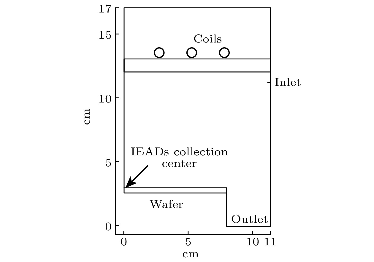
图 1 ICP放电腔室模型
Figure 1. ICP discharge chamber model.

图 2 一维无碰撞鞘层模型示意图
Figure 2. One-dimensional collisionless sheath model schematic diagram.

图 4 刻蚀算法流程图
Figure 4. Etching algorithm flowchart.

图 5 钝化过程中腔室内各粒子的数密度分布 (a) Ar+; (b)
${\text{Cl}}_2^ + $ ; (c) Cl+; (d) Cl自由基Figure 5. Number density distribution of particles in the chamber during passivation process: (a) Ar+; (b)
${\text{Cl}}_2^ + $ ; (c) Cl+; (d) Cl radical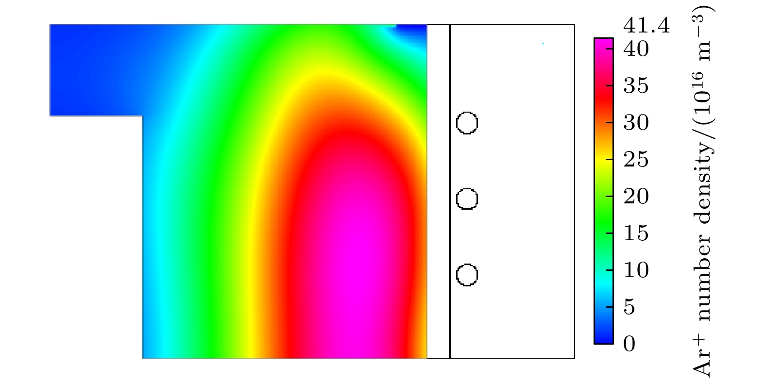
图 6 刻蚀过程中腔室内Ar+离子数密度分布
Figure 6. Number density distribution of Ar+ ions in the chamber during etching process.

图 7 钝化过程中Ar+,
${\text{Cl}}_2^ + $ , Cl+能量分布和角度分布 (a) 能量分布; (b) 角度分布Figure 7. Energy distributions and angular distributions of Ar+,
${\text{Cl}}_2^ + $ and Cl+ during the passivation process: (a) Energy distributions; (b) angular distributions.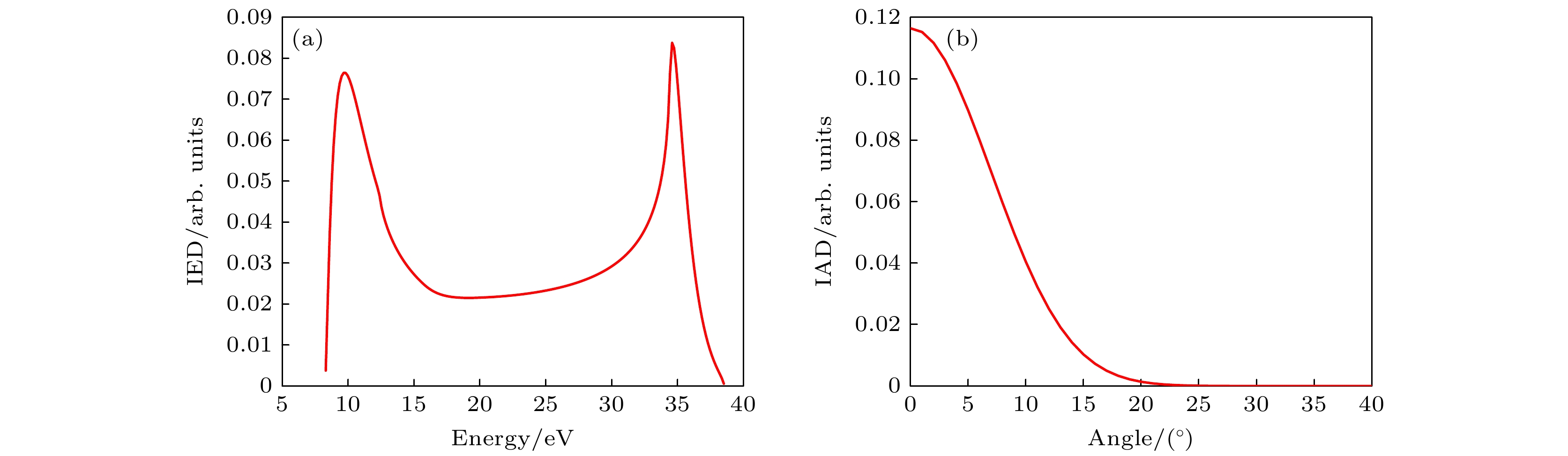
图 8 刻蚀过程中Ar+能量分布和角度分布 (a) 能量分布; (b) 角度分布
Figure 8. Energy distributions and angular distributions of Ar+ during the etching process: (a) Energy distributions; (b) angular distributions.

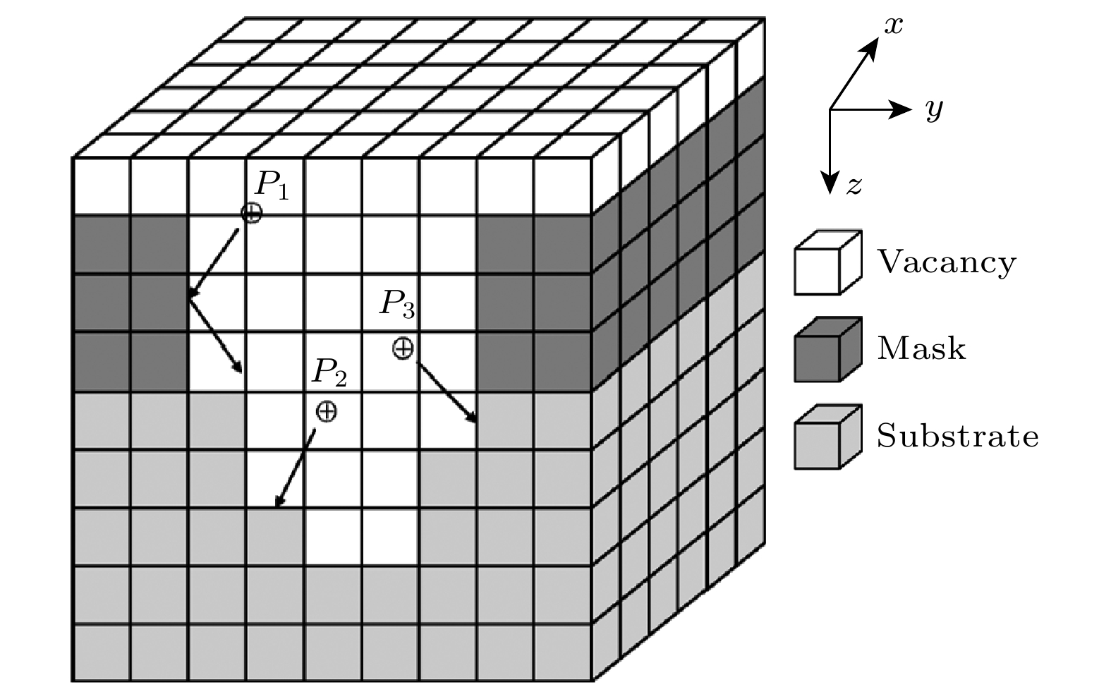
图 9 AR为1的ALE刻蚀沟槽剖面与钝化物云图 (a) AR为1的刻蚀沟槽; (b) 钝化过程中, 四种表面状态的沟槽底部云图
Figure 9. ALE-etched trench with AR of 1 and images of passivated layer: (a) Trench profile with AR of 1; (b) images of the trench bottom showing four different surface states during passivation process.

图 10 AR为1状态下, 钝化过程表面物质占比随时间的变化
Figure 10. Time evolution of surface coverage during passivation process with AR of 1.

图 11 AR为1状态下, 不同条件下启动刻蚀后的表面物质占比随时间的变化曲线 (a) SiCl最多时启动; (b) SiCl2最多时启动; (c) SiCl3最多时启动; (d) 钝化物总和最多时启动
Figure 11. Time evolution of surface composition during etching initiation under different conditions with AR of 1: (a) Initiation with maximum SiCl percentage; (b) initiation with maximum SiCl2 percentage; (c) initiation with maximum SiCl3 percentage; (d) initiation with maximum accumulated passivation species percentage.

图 12 ALE形貌(初始AR为0.5、槽宽60 nm) (a)初始沟槽; (b) 100个循环后的三维ALE沟槽
Figure 12. ALE profile (initial AR of 0.5, trench width of 60 nm): (a) Initial trench; (b) 3D ALE trench after 100 cycles.

图 13 SiCl2占比最多时开始刻蚀所产生的AR与(a)原子层钝化时间、(b)刻蚀时间和(c) ALE单循环时间的变化关系
Figure 13. Evolution of AR with (a) passivation time, (b) etching time, (c) ALE cycle time in the case of SiCl2 dominant etching.
表 1 Si原子层刻蚀多尺度仿真模型对比
Table 1. Summary of Si ALE multi-scale simulation.
ICP
计算模型IEADs
计算模型ALE刻蚀
计算模型研究目标 重点指标 国外 Huard等[5,16] 采用HPEM(2D), 主要包括电磁模块、电子蒙特卡罗模块、流体动力学模块和辐射传输模块 PCMCM
(1D)粒子网格算法元胞法耦合蒙特卡罗法(3D) 统计表面物质占比; 计算ALE协同率和每循环刻蚀深度 非理想的通量和IEADs对ALE的影响; 离子分布不均匀性对ALE的影响 Agarwal和Kushner[15] 元胞法耦合蒙特卡罗法(2D) 分析二维刻蚀剖面形貌 传统的等离子体刻蚀设备即非理想的离子通量对ALE形貌的影响 国内 Ma等[4] 采用商业求解器CFD-ACE+耦合了流体、传热、化学、等离子体和电磁场, 通过有限元方法求解 1D流体模型、蒙特卡罗法 元胞法耦合蒙特卡罗法(2D) 对比IEADs和刻蚀样貌 定制偏压波形对IEADs和刻蚀槽轮廓的影响 本文 元胞法耦合蒙特卡罗法(3D) 统计表面物质占比 ALE最优的钝化和刻蚀时间以及该最优时间随AR的变化规律  DownLoad: CSV
表 2 钝化过程和刻蚀过程中离子和中性基的通量
Table 2. Ion and neutral fluxes during passivation and etching processes.
Ion Flux/(1020 ${{\text{m}}^{ - 2}}{\cdot}{{\text{s}}^{ - 1}}$) Passivation Ar+ 1.762 ${\text{Cl}}_2^ + $ 1.614 Cl+ 1.890 Cl Radical 69.210 Etching Ar+ 21.710
DownLoad: CSV
表 3 AR为1状态下, 刻蚀启动条件不同时完成ALE单循环所需时间以及Si残留占比
Table 3. Time required for completing a single ALE cycle and Si residual ratio under different etching initiation conditions with AR of 1.
Etching initiation
condition (the
largest percentage)SiCl SiCl2 SiCl3 Accumluation Passivation time/s 0.030 0.106 0.550 0.148 Etching time/s 0.296 0.182 0.128 0.155 Total time/s 0.326 0.288 0.678 0.303 Si residual
percent/%17.34 1.35 1.00 1.09
DownLoad: CSV
表 4 ALE刻蚀相同深度的沟槽时间对比
Table 4. Comparison of ALE time for trenches with the same depth.
Total passivation time/s Total etching time/s Number
of ALE
cyclesTotal
ALE
time/sThis paper 2.388 24.520 100 26.908 Ranjan
et al.[14]2.200 38.500 55 40.700
DownLoad: CSV
表 5 AR与原子层刻蚀时间线性拟合的均方根误差(root mean square error, RMSE)和决定系数
Table 5. Root mean square error (RMSE) and coefficient of determination for linear fitting of AR with atomic layer etching time.
Time Passivation time Etching time Total time RMSE 0.018079 0.0052829 0.019098 R2 0.99271 0.99007 0.99478
DownLoad: CSV
-
[1] Jung J, Kim K 2023 Materials 16 3611
Google Scholar
[2] Hao Q, Kim P, Nam S K, Kang S Y, Donnelly V M 2023 J. Vac. Sci. Technol., A 41 032605
Google Scholar
[3] Eliceiri M, Rho Y, Li R, Grigoropoulos C P 2023 J. Vac. Sci. Technol., A 41 022602
Google Scholar
[4] Ma X, Zhang S, Dai Z, Wang Y 2017 Plasma Sci. Technol. 19 085502
Google Scholar
[5] Huard C M, Zhang Y, Sriraman S, Paterson A, Kanarik K J, Kushner M J 2017 J. Vac. Sci. Technol., A 35 031306
Google Scholar
[6] Horiike Y, Tanaka T, Nakano M, Iseda S, Sakaue H, Nagata A, Shindo H, Miyazaki S, Hirose M 1990 J. Vac. Sci. Technol. , A 8 1844
Google Scholar
[7] Matsuura T, Murota J, Sawada Y, Ohmi T 1993 Appl. Phys. Lett. 63 2803
Google Scholar
[8] Imai S, Haga T, Matsuzaki O, Hattori T, Matsumura M 1995 Jpn. J. Appl. Phys., Part 1 34 5049
Google Scholar
[9] Kim J K, Cho S I, Lee S H, Kim C K, Min K S, Kang S H, Yeom G Y 2013 J. Vac. Sci. Technol., A 31 061310
Google Scholar
[10] Song E J, Kim J H, Kwon J D, Kwon S H, Ahn J H 2018 Jpn. J. Appl. Phys. 57 106505
Google Scholar
[11] Goodyear A, Cooke M 2017 J. Vac. Sci. Technol., A 35 01A105
Google Scholar
[12] Yoon M Y, Yeom H J, Kim J H, Chegal W, Cho Y J, Kwon D C, Jeong J R, Lee H C 2021 Phys. Plasmas 28 063504
Google Scholar
[13] Nakamura S, Tanide A, Kimura T, Nadahara S, Ishikawa K, Oda O, Hori M 2023 J. Appl. Phys. 133 043302
Google Scholar
[14] Ranjan A, Wang M, Sherpa S D, Rastogi V, Koshiishi A, Ventzek P L G 2016 J. Vac. Sci. Technol., A 34 031304
Google Scholar
[15] Agarwal A, Kushner M J 2009 J. Vac. Sci. Technol., A 27 37
Google Scholar
[16] Huard C M, Lanham S J, Kushner M J 2018 J. Phys. D: Appl. Phys. 51 155201
Google Scholar
[17] 贺平逆, 宁建平, 秦尤敏, 赵成利, 苟富均 2011 物理学报 60 045209
Google Scholar
He P N, Ning J P, Qin Y M, Zhao C L, Gou F J 2011 Acta Phys. 60 045209
Google Scholar
[18] Vella J R, Humbird D, Graves D B 2022 J. Vac. Sci. Technol., B 40 023205
Google Scholar
[19] Sui J, Zhang S, Liu Z, Yan J, Dai Z 2016 Plasma Sci. Technol. 18 666
Google Scholar
[20] 葛婕 2014 硕士学位论文 (北京: 清华大学)
Ge J 2014 M. S. Thesis (Beijing: Tsinghua University
[21] Brezmes A O, Breitkopf C 2015 Vacuum 116 65
Google Scholar
[22] Liu Z L, Jing X B, Yao K L 2005 J. Phys. D: Appl. Phys. 38 1899
Google Scholar
[23] 杨宏军, 宋亦旭, 郑树琳, 贾培发 2013 物理学报 62 208201
Google Scholar
Yang H J, Song Y X, Zheng S L, Jia P F 2013 Acta Phys. Sin. 62 208201
Google Scholar
[24] 高扬福, 宋亦旭, 孙晓民 2014 物理学报 63 048201
Google Scholar
Gao Y F, Song Y X, Sun X M 2014 Acta Phys. Sin. 63 048201
Google Scholar
[25] 郑树琳, 宋亦旭, 孙晓民 2013 物理学报 62 108201
Google Scholar
Zheng S L, Song Y X, Sun X M 2013 Acta Phys. Sin. 62 108201
Google Scholar
[26] Huard C M, Zhang Y, Sriraman S, Paterson A, Kushner M J 2017 J. Vac. Sci. Technol. , A 35 05C301
Google Scholar
[27] Han J, Pribyl P, Gekelman W, Paterson A, Lanham S J, Qu C, Kushner M J 2019 Phys. Plasmas 26 103503
Google Scholar
[28] Kushner M J 2009 J. Phys. D: Appl. Phys. 42 194013
Google Scholar

 DownLoad:


Catalog
Metrics
- Abstract views: 1214
- PDF Downloads: 61
- Cited By: 0
