-
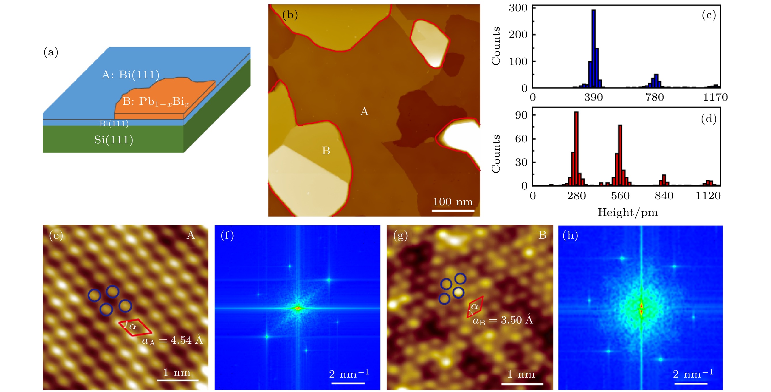
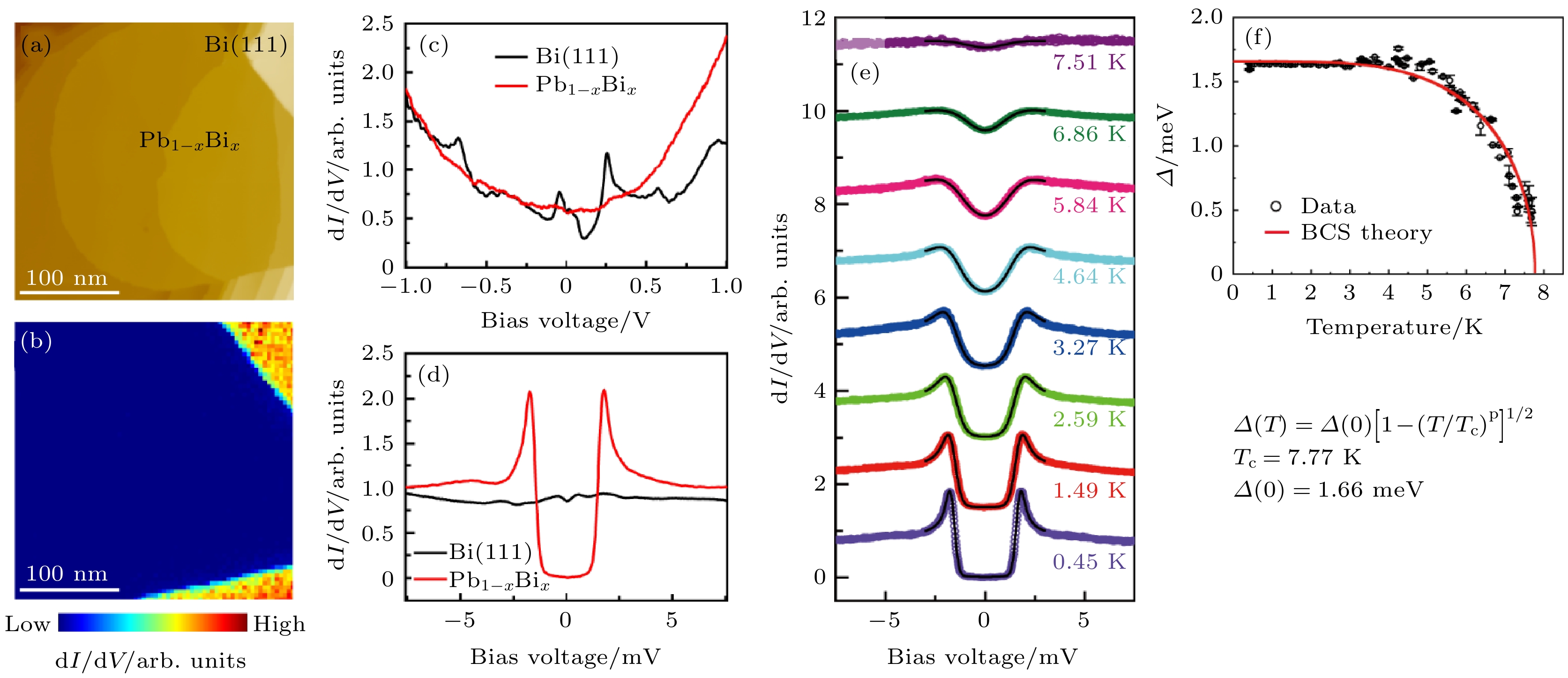
Lead-bismuth (Pb-Bi) alloys, as a superconducting material, have been widely studied at their superconducting transition temperatures and the critical magnetic fields for different composition ratios. Most of experimental studies focused on the stable ε phase formed at high temperatures, but less on the Pb-Bi alloys grown at low temperatures. So far, the structural and superconducting properties of the low-temperature Pb-Bi phases are far from good understanding. Here, we report our investigation of structural and superconducting properties of a low-temperature phase of Pb-Bi alloy. The Pb-Bi alloy films with a nominal thickness of about 6 nm are prepared by co-depositing Bi and Pb on Bi(111)/Si(111)-(7 × 7) substrates at a low temperature of 100 K followed by annealing at a treatment of 200 K for 2 h. The structural and superconducting properties of the Pb-Bi alloy films are characterized in situ by using low-temperature scanning tunneling microscopy/spectroscopy (STM/STS). It is observed that the spatially separated phases of nearly pure Bi(111) domains and Pb1–xBix alloy domains are formed in the films, where these phases can be identified by their distinct differences in the atomic structure and the distributions of step heights in the atomically resolved STM images, as well as by their distinguished STS spectra. The Pb1–xBix alloy phase presents the structure of Pb(111), in which about x ≈ 0.1 Bi is substituted for Pb. The STS spectra show that the Pb1–xBix alloy phase is superconducting, with a transition temperature Tc = 7.77 K derived from the variable-temperature measurements. This transition temperature is higher than that in pure Pb film (6.0–6.5 K), which can be well explained by the Mattias rules, with considering the fact that the average number of valance electrons increases after Bi atoms with five valance-electrons have been substituted for Pb atoms with four valance-electrons. The analysis shows that the ratio
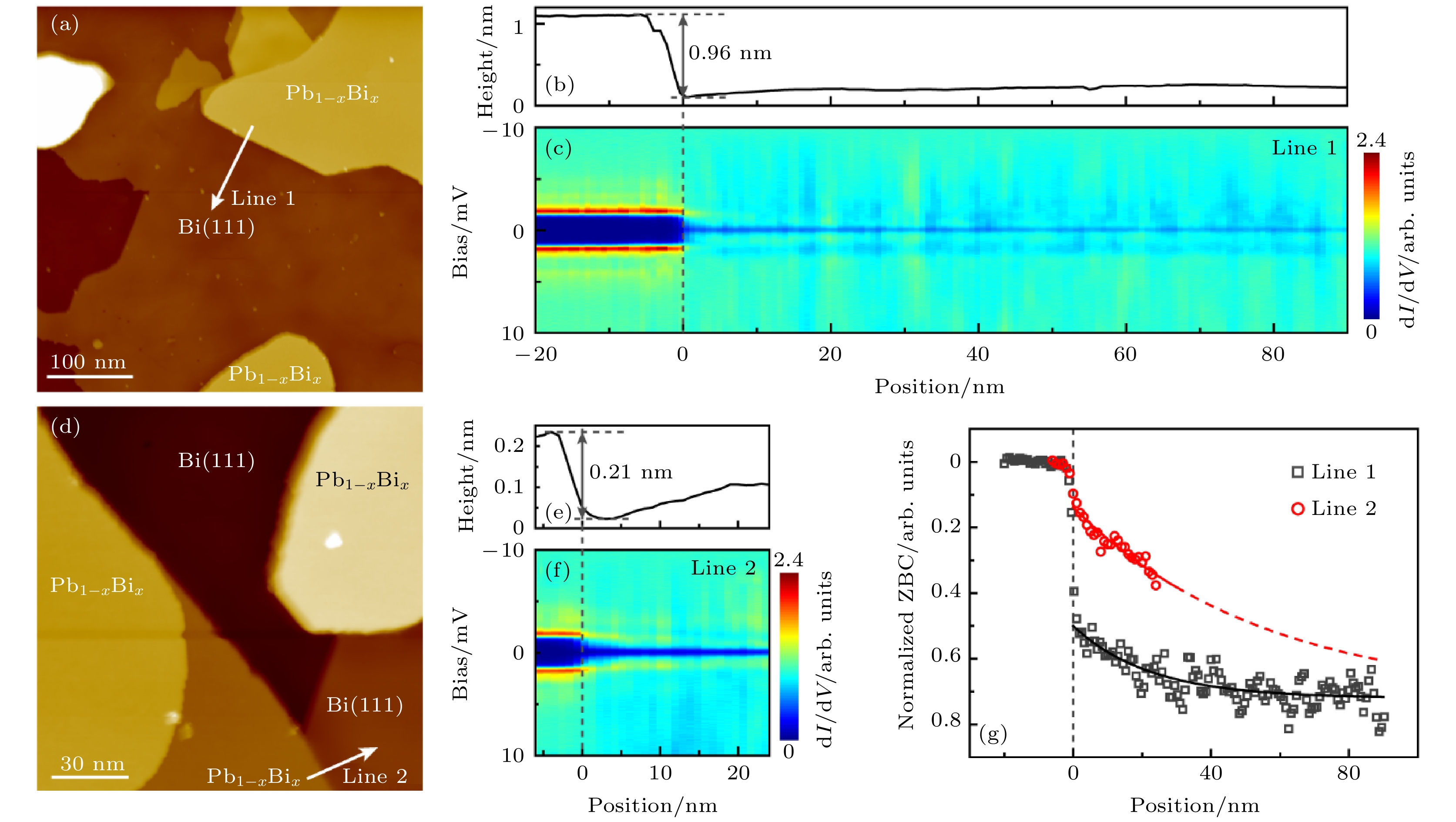
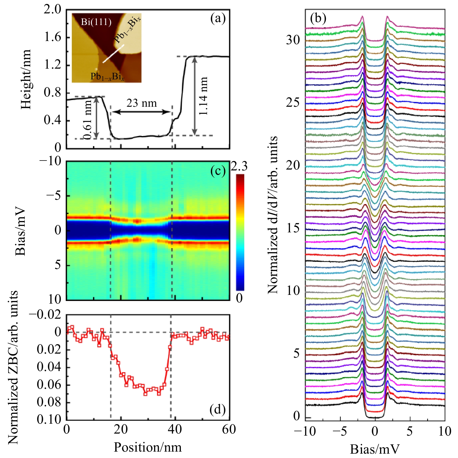
$ 2\Delta (0)/{k_{\rm{B}}}{T_{\rm{C}}}$ is about 4.94 with the superconducting gap$ \varDelta (0) = 1.66$ meV at 0 K, indicating that the Pb1–xBix alloy is a strongly-coupled superconductor. The non-superconducting Bi(111) and the superconducting Pb1–xBix alloy domains form an in-plane superconductor-normal metal-superconductor (S-N-S) Josephson junction. The proximity effect in the Bi(111) domains is measured at different N-S junctions, which suggests that the lateral superconducting penetration length in Bi(111) might be affected by the area of the quasi-two-dimensional interface. The superconducting gap in the Bi(111) region with a narrow width of 23 nm in an S-N-S Josephson junction is found to be greatly enhanced due to the existence of multiple Andreev reflections. Since Bi can host potential topological properties, the lateral Bi(111)-Pb1–xBix heterostructures, because of the existing proximity effect, could have potential applications in exploring the novel topological and superconducting phenomena.-
Keywords:
- bismuth-lead alloy /
- superconducting transition temperature /
- proximity effect /
- scanning tunneling microscopy
[1] 张志模, 张文号, 付英双 2019 物理学报 68 226801
 Google Scholar
Zhang Z M, Zhang W H, Fu Y S 2019 Acta Phys. Sin. 68 226801
 Google Scholar
[2] 张玺, 刘超飞, 王健 2015 物理学报 64 217405
 Google Scholar
Zhang X, Liu C F, Wang J 2015 Acta Phys. Sin. 64 217405
 Google Scholar
[3] Adler J, Ng S 1965 Can. J. Phys. 43 594
 Google Scholar
[4] Chen T T, Leslie J D, Smith H J T 1971 Physica 55 439
 Google Scholar
[5] Dynes R C, Rowell J M 1975 Phys. Rev. B 11 1884
 Google Scholar
[6] Özer M M, Jia Y, Zhang Z Y, Thompson J R, Weitering H H 2007 Science 316 1594
 Google Scholar
[7] Egami T, Waseda Y 1984 J. Non-cryst. Solids 64 113
 Google Scholar
[8] Gokcen N A 1992 J. Phase Equilib. 13 21
 Google Scholar
[9] Gandhi A C, Chan T S, Wu S Y 2017 Supercond. Sci. Technol. 30 105010
 Google Scholar
[10] Strukov G V, Stolyarov V S, Strukova G K, Zverev V N 2012 Physica C 483 162
 Google Scholar
[11] Gandhi A C, Wu S Y 2016 J. Magn. Magn. Mater. 407 155
 Google Scholar
[12] King H W, Russell C M, Hulbert J A 1966 Phys. Lett. 20 600
 Google Scholar
[13] Stolyarov V S, Zverev V N, Postnova E Y, Strukov G V, Strukova G K, Rusanov A Y, Shmitko I M 2012 J. Nanosci. Nanotechnol. 12 4991
 Google Scholar
[14] Kuo C G, Lo S C, Chen J H, Chiang C C, Chao C G 2005 Jpn. J. Appl. Phys. 44 3333
 Google Scholar
[15] Fujime S 1966 Jpn. J. Appl. Phys. 5 59
 Google Scholar
[16] Borromee G C, Giessen B C, Grant N J 1968 J. Chem. Phys. 48 1905
 Google Scholar
[17] Matthias B T 1955 Phys. Rev. 97 74
 Google Scholar
[18] Brun C, Cren T, Cherkez V, Debontridder F, Pons S, Fokin D, Tringides M C, Bozhko S, Ioffe L B, Altshuler B L, Roditchev D 2014 Nat. Phys. 10 444
 Google Scholar
[19] Yoshizawa S, Kim H, Kawakami T, Nagai Y, Nakayama T, Hu X, Hasegawa Y, Uchihashi T 2014 Phys. Rev. Lett. 113 247004
 Google Scholar
[20] Andreev A F 1964 J. Exp. Theor. Phys. 46 1823
[21] Du H, Sun X, Liu X, Wu X, Wang J, Tian M, Zhao A, Luo Y, Yang J, Wang B, Hou J G 2016 Nat. Commun. 7 10814
 Google Scholar
[22] Dynes R C, Narayanamurti V, Garno J P 1978 Phys. Rev. Lett. 41 1509
 Google Scholar
[23] Hofmann Ph 2006 Prog. Surf. Sci. 81 191
 Google Scholar
[24] Hirahara T, Nagao T, Matsuda I, Bihlmayer G, Chulkov E, Koroteev Y M, Echenique P, Saito M, Hasegawa S 2006 Phys. Rev. Lett. 97 146803
 Google Scholar
[25] Hirahara T, Nagao T, Matsuda I, Bihlmayer G, Chulkov E V, Koroteev Y M, Hasegawa S 2007 Phys. Rev. B 75 035422
 Google Scholar
[26] Eom D, Qin S, Chou M Y, Shih C K 2006 Phys. Rev. Lett. 96 027005
 Google Scholar
[27] Kim J, Chua V, Fiete G A, Nam H, MacDonald A H, Shih C K 2012 Nat. Phys. 8 464
 Google Scholar
[28] Usadel K D 1970 Phys. Rev. Lett. 25 507
 Google Scholar
[29] Cherkez V, Cuevas J C, Brun C, Cren T, Ménard G, Debontridder F, Stolyarov V S, Roditchev D 2014 Phys. Rev. X 4 011033
 Google Scholar
[30] Kim H, Lin S Z, Graf M J, Miyata Y, Nagai Y, Kato T, Hasegawa Y 2016 Phys. Rev. Lett. 117 116802
 Google Scholar
[31] Kim H, Miyata Y, Hasegawa Y 2016 Supercond. Sci. Technol. 29 084006
 Google Scholar
[32] Wang M X, Liu C H, Xu J P, Yang F, Miao L, Yao M Y, Gao C L, Shen C Y, Ma X C, Chen X, Xu Z A, Liu Y, Zhang S C, Qian D, Jia J F, Xue Q K 2012 Science 336 52
 Google Scholar
[33] Zareapour P, Hayat A, Zhao S Y F, Kreshchuk M, Jain A, Kwok D C, Lee N, Cheong S W, Xu Z, Yang A, Gu G D, Jia S, Cava R J, Burch K S 2012 Nat. Commun. 3 1056
 Google Scholar
[34] Wang E Y, Ding H, Fedorov A V, Yao W, Li Z, Lv Y F, Zhao K, Zhang L G, Xu Z J, Schneeloch J, Zhong R D, Ji S H, Wang L L, He K, Ma X C, Gu G D, Yao H, Xue Q K, Chen X, Zhou S Y 2013 Nat. Phys. 9 621
 Google Scholar
[35] Xu J P, Liu C, Wang M X, Ge J, Liu Z L, Yang X, Chen Y, Liu Y, Xu Z A, Gao C L, Qian D, Zhang F C, Jia J F 2014 Phys. Rev. Lett. 112 217001
 Google Scholar
[36] Xu J P, Wang M X, Liu Z L, Ge J F, Yang X, Liu C, Xu Z A, Guan D, Gao C L, Qian D, Liu Y, Wang Q H, Zhang F C, Xue Q K, Jia J F 2015 Phys. Rev. Lett. 114 017001
 Google Scholar
[37] Fu L, Kane C L 2008 Phys. Rev. Lett. 100 096407
 Google Scholar
[38] Wang D, Kong L, Fan P, Chen H, Zhu S, Liu W, Cao L, Sun Y, Du S, Schneeloch J, Zhong R, Gu G, Fu L, Ding H, Gao H J 2018 Science 362 333
 Google Scholar
[39] Zhu S, Kong L, Cao L, Chen H, Papaj M, Du S, Xing Y, Liu W, Wang D, Shen C, Yang F, Schneeloch J, Zhong R, Gu G, Fu L, Zhang Y Y, Ding H, Gao H J 2020 Science 367 189
 Google Scholar
-
图 1 Pb1–xBix合金薄膜的生长与结构表征 (a) 在Bi(111)/Si(111)-(7 × 7)衬底低温共沉积铅铋原子得到的样品结构示意图; (b) 样品表面大范围的STM图像; (c), (d) A和B区域台阶高度分布统计的结果(统计不同区域大范围图像约110幅); (e), (f) A区域的STM原子图像及其快速傅里叶变换(fast Fourier transform, FFT)图谱; (g), (h) B区域的STM原子图像及其FFT图谱. 扫描条件: (b) 样品偏压Vs = –1 V, 隧穿电流It = 20 pA, 扫描尺寸为500 nm × 500 nm; (e) Vs = –20 mV, It = 2 nA; (g) Vs = 5 mV, It = 1 nA, 扫描尺寸为4 nm × 4 nm
Figure 1. Growth of the Pb1–xBix alloy film and characterization of surface structures: (a) Schematics of the Pb-Bi alloy film grown on Bi(111)/Si(111)-(7 × 7) substrate; (b) STM topography image of the alloy surface (500 nm × 500 nm, sample bias Vs = –1 V and tunneling current It = 20 pA); (c) and (d) step height distribution of A and B phases counted in around 110 images; (e) and (f) atomically-resolved STM image and corresponding fast Fourier transform (FFT) pattern of the A phase (Vs = –20 mV and It = 2 nA, 4 nm × 4 nm); (g) and (h) atomically-resolved STM image and corresponding FFT pattern of the B phase (Vs = 5 mV and It = 1 nA, 4 nm × 4 nm).
图 2 Pb1–xBix合金薄膜的超导物性表征 (a), (b) STM拓扑图及其相同区域无磁场时的零偏压电导像, STM扫描条件: Vs = –90 mV, It = 20 pA, 扫描尺寸为280 nm × 280 nm. (c), (d) 4.2和0.4 K下在Bi(111)(黑线)和Pb1–xBix(红线)表面区域采集的不同能量范围的典型dI/dV谱, 采谱条件: (c) Vs = –1 V, It = 2 nA, 调制偏压Vmod = 2 mV; (d) Vs = –10 mV, It = 1 nA, Vmod = 100 μV. (e) 不同温度下dI/dV谱, 叠加在实验谱线上的黑线段(± 3 mV)是基于BCS理论对能隙的拟合. 采谱条件: Vs = –10 mV, It = 1 nA, Vmod = 100 μV; (f)超导能隙大小和温度的依赖关系及拟合结果
Figure 2. Electronic properties of the Bi(111) and Pb1–xBix phases: (a) STM image (280 nm × 280 nm) of the Pb-Bi alloy surface; (b) zero-bias conductance (ZBC) image acquired within the same area in Fig. (a); (c), (d) representative dI/dV spectra of the Bi(111) region (black line) and Pb1–xBix region (red line) measured with a W tip at 4.2 and 0.4 K in different energy ranges, respectively; (e) temperature-dependent dI/dV spectra, overlaid with the fitting segments (in black) on the basis of BCS theory, and the spectra are shifted vertically for clarity; (f) temperature dependence of the superconducting energy gap extracted from Fig. (e) (black circle) and fitting with temperature-dependent superconducting gap ∆(T) (red line) using BCS theory.
图 3 正常金属-超导体(N-S)异质结处的邻近效应 (a) 合金表面大面积STM图像, 扫描条件为Vs = –98 mV, It = 20 pA, 450 nm × 450 nm. (b) 沿图(a)中白色带箭头直线(Line 1)得到的N-S异质结表面高度轮廓线, 显示异质结两侧高度差约为960 pm. (c) 沿Line 1所采的dI/dV谱经归一化后画成的二维电导图, 采谱间隔为0.75 nm, 采谱条件为Vs = –10 mV, It = 1 nA, Vmod = 100 μV. (d) 合金表面大面积STM图像, 扫描条件为Vs = –1 V, It = 20 pA, 150 nm × 150 nm. (e) 沿图(d)中白色带箭头直线(Line 2)得到的N-S异质结表面高度轮廓线, 显示异质结两侧高度差约为210 pm. (f) 由沿Line 2所采的dI/dV谱经归一化后画成的二维电导图, 采谱间隔为1 nm, 采谱条件为Vs = –10 mV, It = 1 nA, Vmod = 100 μV. 在图(c)和图(f)中, 所有谱已根据Vs = –10 mV处的电导做了归一化. (g) 沿Line 1和Line 2的归一化零偏压电导随位置的依赖关系. 图中实线为指数衰减公式拟合结果, 红色: –0.58 e–y/55.23 + 0.72, 黑色: –0.22 e–y/22.33 + 0.72, y是距离台阶下边缘的位置坐标
Figure 3. Proximity effect at normal metal-superconductor (N-S) heterojunctions: (a) Large-area STM image of the alloy surface (Vs = –98 mV, It = 20 pA, 450 nm × 450 nm). (b) Height profile along the white-arrowed Line 1 as marked in Fig. (a). (c) Two-dimensional (2D) conductance map plotted with normalized dI/dV spectra acquired across the N-S heterojunction along Line 1 with a spacing of 0.75 nm (Vs = –10 mV, It = 1 nA, Vmod = 100 μV). (d) Large-area STM image of the alloy surface (Vs = –1 V, It = 20 pA, 150 nm × 150 nm). (e) Height profile along the white-arrowed Line 2 in Fig. (d). (f) 2D conductance map plotted with normalized dI/dV spectra acquired across the N-S heterojunction along Line 2 with a spacing of 1 nm (Vs = –10 mV, It = 1 nA, Vmod = 100 μV). In Fig. (c) and Fig. (f), the conductance at the setpoint bias (Vs = –10 mV) in the dI/dV curves is normalized to 1. (g) Plots of the normalized zero-bias conductance (ZBC) along Line 1 (black rectangles) and Line 2 (red circles). The red and black curves are exponential fittings of the data with functions as –0.58 e–y/55.23 + 0.72 and –0.22 e–y/22.33 + 0.72, respectively. y is the distance away from the lower step edge.
图 4 超导体-正常金属-超导体(S-N-S)异质结中的邻近效应 (a) 沿着插图所示白线得到的S-N-S异质结高度轮廓线, 插图是与图3(d)相同的铅铋合金表面STM图像, 扫描条件为Vs = –1 V, It = 20 pA, 150 nm × 150 nm; (b) 沿图(a)中白线所采的归一化后的61条dI/dV谱, 采谱间隔1 nm, 采谱条件为Vs = –10 mV, It = 1 nA, Vmod = 100 μV; (c) 由图(b)所示的归一化dI/dV谱画成的二维微分电导图; (d) 从图(c)中得到的S-N-S异质结中零偏压电导随位置的变化
Figure 4. Proximity effect at the superconductor-normal metal-superconductor (S-N-S) heterojunction: (a) Height profile of the S-N-S heterojunction along the white line shown in the inset STM image, which is the same as Fig. 3(d) (Vs = –1 V, It = 20 pA, 150 nm × 150 nm); (b) normalized dI/dV curves acquired across the S-N-S heterojunction along the white line in Fig. (a) with a spacing of 1 nm (Vs = –10 mV, It = 1 nA, Vmod = 100 μV); (c) 2D conductance map plotted with the normalized dI/dV spectra in Fig. (b); (d) plot of the site-dependent ZBC in Fig. (c) along the S-N-S heterojunction.
-
[1] 张志模, 张文号, 付英双 2019 物理学报 68 226801
 Google Scholar
Zhang Z M, Zhang W H, Fu Y S 2019 Acta Phys. Sin. 68 226801
 Google Scholar
[2] 张玺, 刘超飞, 王健 2015 物理学报 64 217405
 Google Scholar
Zhang X, Liu C F, Wang J 2015 Acta Phys. Sin. 64 217405
 Google Scholar
[3] Adler J, Ng S 1965 Can. J. Phys. 43 594
 Google Scholar
[4] Chen T T, Leslie J D, Smith H J T 1971 Physica 55 439
 Google Scholar
[5] Dynes R C, Rowell J M 1975 Phys. Rev. B 11 1884
 Google Scholar
[6] Özer M M, Jia Y, Zhang Z Y, Thompson J R, Weitering H H 2007 Science 316 1594
 Google Scholar
[7] Egami T, Waseda Y 1984 J. Non-cryst. Solids 64 113
 Google Scholar
[8] Gokcen N A 1992 J. Phase Equilib. 13 21
 Google Scholar
[9] Gandhi A C, Chan T S, Wu S Y 2017 Supercond. Sci. Technol. 30 105010
 Google Scholar
[10] Strukov G V, Stolyarov V S, Strukova G K, Zverev V N 2012 Physica C 483 162
 Google Scholar
[11] Gandhi A C, Wu S Y 2016 J. Magn. Magn. Mater. 407 155
 Google Scholar
[12] King H W, Russell C M, Hulbert J A 1966 Phys. Lett. 20 600
 Google Scholar
[13] Stolyarov V S, Zverev V N, Postnova E Y, Strukov G V, Strukova G K, Rusanov A Y, Shmitko I M 2012 J. Nanosci. Nanotechnol. 12 4991
 Google Scholar
[14] Kuo C G, Lo S C, Chen J H, Chiang C C, Chao C G 2005 Jpn. J. Appl. Phys. 44 3333
 Google Scholar
[15] Fujime S 1966 Jpn. J. Appl. Phys. 5 59
 Google Scholar
[16] Borromee G C, Giessen B C, Grant N J 1968 J. Chem. Phys. 48 1905
 Google Scholar
[17] Matthias B T 1955 Phys. Rev. 97 74
 Google Scholar
[18] Brun C, Cren T, Cherkez V, Debontridder F, Pons S, Fokin D, Tringides M C, Bozhko S, Ioffe L B, Altshuler B L, Roditchev D 2014 Nat. Phys. 10 444
 Google Scholar
[19] Yoshizawa S, Kim H, Kawakami T, Nagai Y, Nakayama T, Hu X, Hasegawa Y, Uchihashi T 2014 Phys. Rev. Lett. 113 247004
 Google Scholar
[20] Andreev A F 1964 J. Exp. Theor. Phys. 46 1823
[21] Du H, Sun X, Liu X, Wu X, Wang J, Tian M, Zhao A, Luo Y, Yang J, Wang B, Hou J G 2016 Nat. Commun. 7 10814
 Google Scholar
[22] Dynes R C, Narayanamurti V, Garno J P 1978 Phys. Rev. Lett. 41 1509
 Google Scholar
[23] Hofmann Ph 2006 Prog. Surf. Sci. 81 191
 Google Scholar
[24] Hirahara T, Nagao T, Matsuda I, Bihlmayer G, Chulkov E, Koroteev Y M, Echenique P, Saito M, Hasegawa S 2006 Phys. Rev. Lett. 97 146803
 Google Scholar
[25] Hirahara T, Nagao T, Matsuda I, Bihlmayer G, Chulkov E V, Koroteev Y M, Hasegawa S 2007 Phys. Rev. B 75 035422
 Google Scholar
[26] Eom D, Qin S, Chou M Y, Shih C K 2006 Phys. Rev. Lett. 96 027005
 Google Scholar
[27] Kim J, Chua V, Fiete G A, Nam H, MacDonald A H, Shih C K 2012 Nat. Phys. 8 464
 Google Scholar
[28] Usadel K D 1970 Phys. Rev. Lett. 25 507
 Google Scholar
[29] Cherkez V, Cuevas J C, Brun C, Cren T, Ménard G, Debontridder F, Stolyarov V S, Roditchev D 2014 Phys. Rev. X 4 011033
 Google Scholar
[30] Kim H, Lin S Z, Graf M J, Miyata Y, Nagai Y, Kato T, Hasegawa Y 2016 Phys. Rev. Lett. 117 116802
 Google Scholar
[31] Kim H, Miyata Y, Hasegawa Y 2016 Supercond. Sci. Technol. 29 084006
 Google Scholar
[32] Wang M X, Liu C H, Xu J P, Yang F, Miao L, Yao M Y, Gao C L, Shen C Y, Ma X C, Chen X, Xu Z A, Liu Y, Zhang S C, Qian D, Jia J F, Xue Q K 2012 Science 336 52
 Google Scholar
[33] Zareapour P, Hayat A, Zhao S Y F, Kreshchuk M, Jain A, Kwok D C, Lee N, Cheong S W, Xu Z, Yang A, Gu G D, Jia S, Cava R J, Burch K S 2012 Nat. Commun. 3 1056
 Google Scholar
[34] Wang E Y, Ding H, Fedorov A V, Yao W, Li Z, Lv Y F, Zhao K, Zhang L G, Xu Z J, Schneeloch J, Zhong R D, Ji S H, Wang L L, He K, Ma X C, Gu G D, Yao H, Xue Q K, Chen X, Zhou S Y 2013 Nat. Phys. 9 621
 Google Scholar
[35] Xu J P, Liu C, Wang M X, Ge J, Liu Z L, Yang X, Chen Y, Liu Y, Xu Z A, Gao C L, Qian D, Zhang F C, Jia J F 2014 Phys. Rev. Lett. 112 217001
 Google Scholar
[36] Xu J P, Wang M X, Liu Z L, Ge J F, Yang X, Liu C, Xu Z A, Guan D, Gao C L, Qian D, Liu Y, Wang Q H, Zhang F C, Xue Q K, Jia J F 2015 Phys. Rev. Lett. 114 017001
 Google Scholar
[37] Fu L, Kane C L 2008 Phys. Rev. Lett. 100 096407
 Google Scholar
[38] Wang D, Kong L, Fan P, Chen H, Zhu S, Liu W, Cao L, Sun Y, Du S, Schneeloch J, Zhong R, Gu G, Fu L, Ding H, Gao H J 2018 Science 362 333
 Google Scholar
[39] Zhu S, Kong L, Cao L, Chen H, Papaj M, Du S, Xing Y, Liu W, Wang D, Shen C, Yang F, Schneeloch J, Zhong R, Gu G, Fu L, Zhang Y Y, Ding H, Gao H J 2020 Science 367 189
 Google Scholar
Catalog
Metrics
- Abstract views: 10854
- PDF Downloads: 213
- Cited By: 0


 DownLoad:


