


Highlights
SPECIAL TOPIC—Research progress on nickelate superconductors·COVER ARTICLE
COVER ARTICLE
2025, 74 (22): 227403.
doi: 10.7498/aps.74.20251080
Abstract +
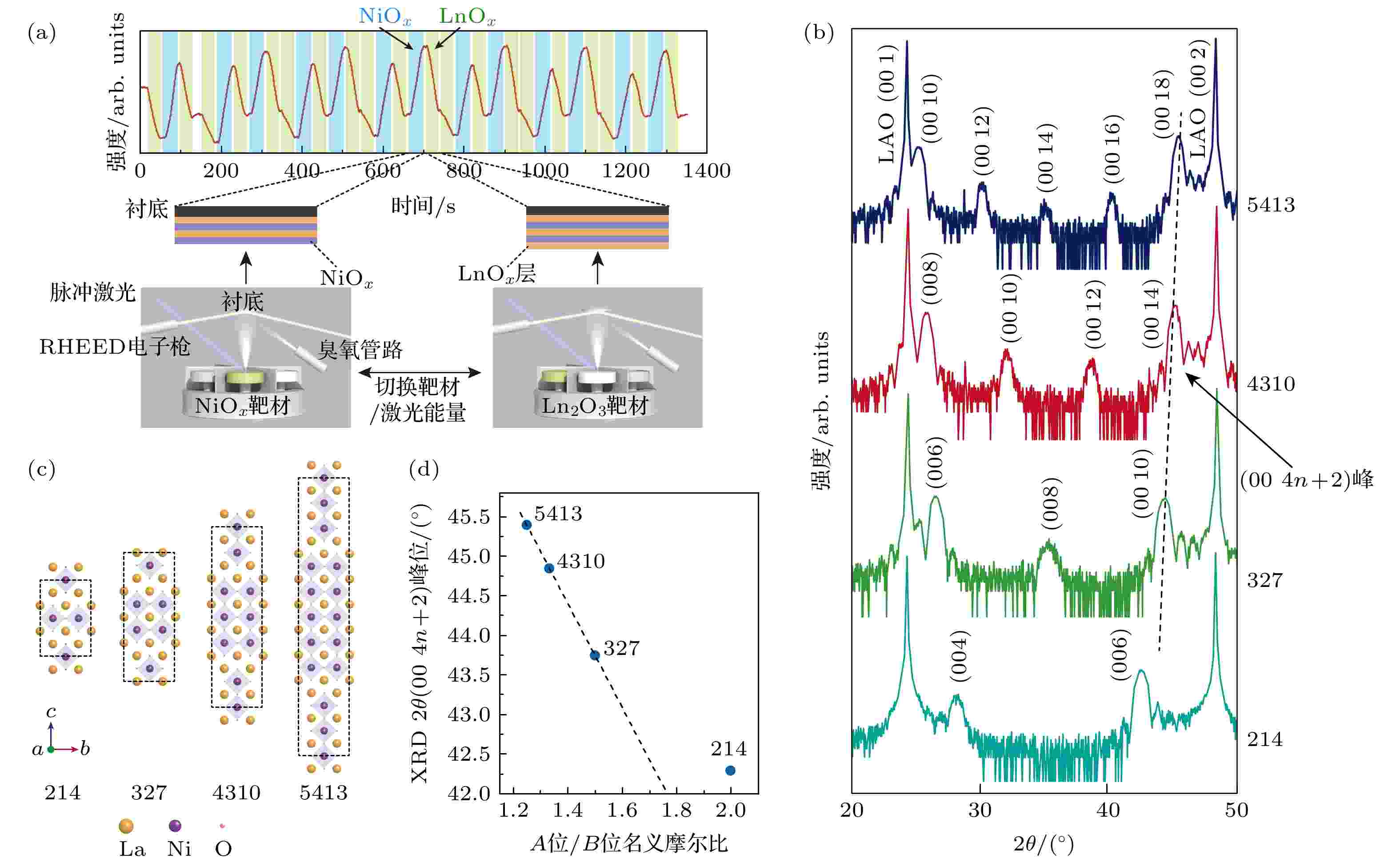
The discovery of ambient-pressure nickelate high-temperature superconductivity provides a new platform for further exploring the underlying superconducting mechanisms. However, the thermodynamic metastability of Ruddlesden-Popper nickelates Lnn+1NinO3n+1 (Ln = lanthanide) poses significant challenges for precise control over their structures and oxygen stoichiometry. This study establishes a systematic approach to growing phase-pure, high-quality Ln3Ni2O7 thin films on LaAlO3 and SrLaAlO4 substrates by using gigantic-oxidative atomic-layer-by-layer epitaxy. The films grown under an ultrastrong oxidizing ozone atmosphere are superconducting without further post-annealing. Specifically, the optimal Ln3Ni2O7/SrLaAlO4 superconducting film exhibits an onset transition temperature (Tc,onset) of 50 K. Four critical factors governing the crystalline quality and superconducting properties of Ln3Ni2O7 films are identified as follows. 1) Precise cation stoichiometric control suppresses secondary phase formation. In an Ni-rich sample (+7%), the thin film forms an Ln4Ni3O10 secondary phase, and the R-T curve correspondingly exhibits metallic behavior. In contrast, an Ni-deficient sample forms an Ln2NiO4 secondary phase, with its R-T curve indicating insulating behavior over the entire temperature range. 2) Complete atomic layer-by-layer coverage minimizes stacking faults. Deviation from ideal monolayer coverage induces in-plane atomic number mismatch, which directly triggers out-of-plane lattice collapse or uplift near bulk-equilibrium positions. 3) Optimized interface reconstruction can improve the atomic arrangement at the interface. This can be achieved through methods such as annealing the SrLaAlO4 substrate or pre-depositing a 0.5-unit-cell-thick Ln2NiO4-phase buffer layer, which enhances the energy difference between the Ln-site and Ni-site layers to promote proper stacking. 4) Accurate oxygen content regulation is essential for achieving a single superconducting transition and high Tc,onset. Although the under-oxidized sample demonstrates a relatively high Tc,onset (50 K), it displays a two-step superconducting transition. Conversely, the over-oxidized sample exhibits a reduced Tc,onset of 37 K and similarly manifests a two-step transition. These findings provide valuable insights into the layer-by-layer epitaxy growth of diverse oxide high-temperature superconducting films.


SPECIAL TOPIC—Research progress on nickelate superconductors
EDITOR'S SUGGESTION
2025, 74 (22): 227401.
doi: 10.7498/aps.74.20251179
Abstract +
SPECIAL TOPIC—Research progress on nickelate superconductors
EDITOR'S SUGGESTION
2025, 74 (22): 227402.
doi: 10.7498/aps.74.20251258
Abstract +
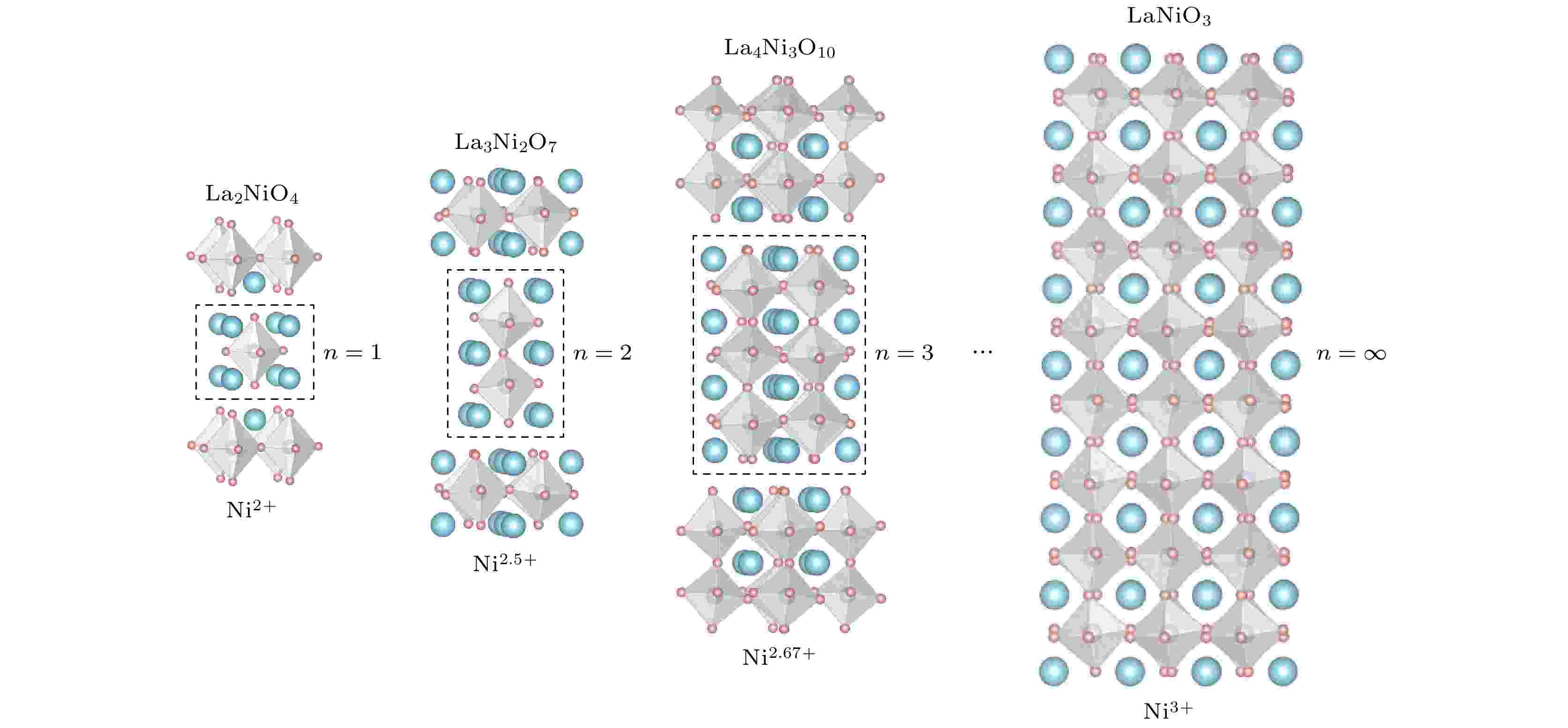
The recent discovery of high-temperature superconductivity in the bilayer nickelate La3Ni2O7 under high pressure has drawn significant attention, further catalyzing intensive research on nickel-based superconductors. Systematic comparative studies of unconventional superconductors are vital for advancing the mechanistic understanding of high-Tc superconductivity. In contrast to cuprates, bulk nickelates exhibit significant differences in crystal structure, electronic properties, and physical behaviors, and their experimental investigation faces specific challenges including the influences of hydrostatic conditions on the measurements of zero resistance and diamagnetic response, oxygen vacancy defects in single crystals, and pressure-induced structural phase transitions. This review comprehensively examines high-temperature superconductivity and the related research challenges in trilayer nickelate bulk materials, and provides experimental insights for future studies on nickel-based superconducting systems.
SPECIAL TOPIC—Research progress on nickelate superconductors
EDITOR'S SUGGESTION
2025, 74 (22): 227404.
doi: 10.7498/aps.74.20250903
Abstract +
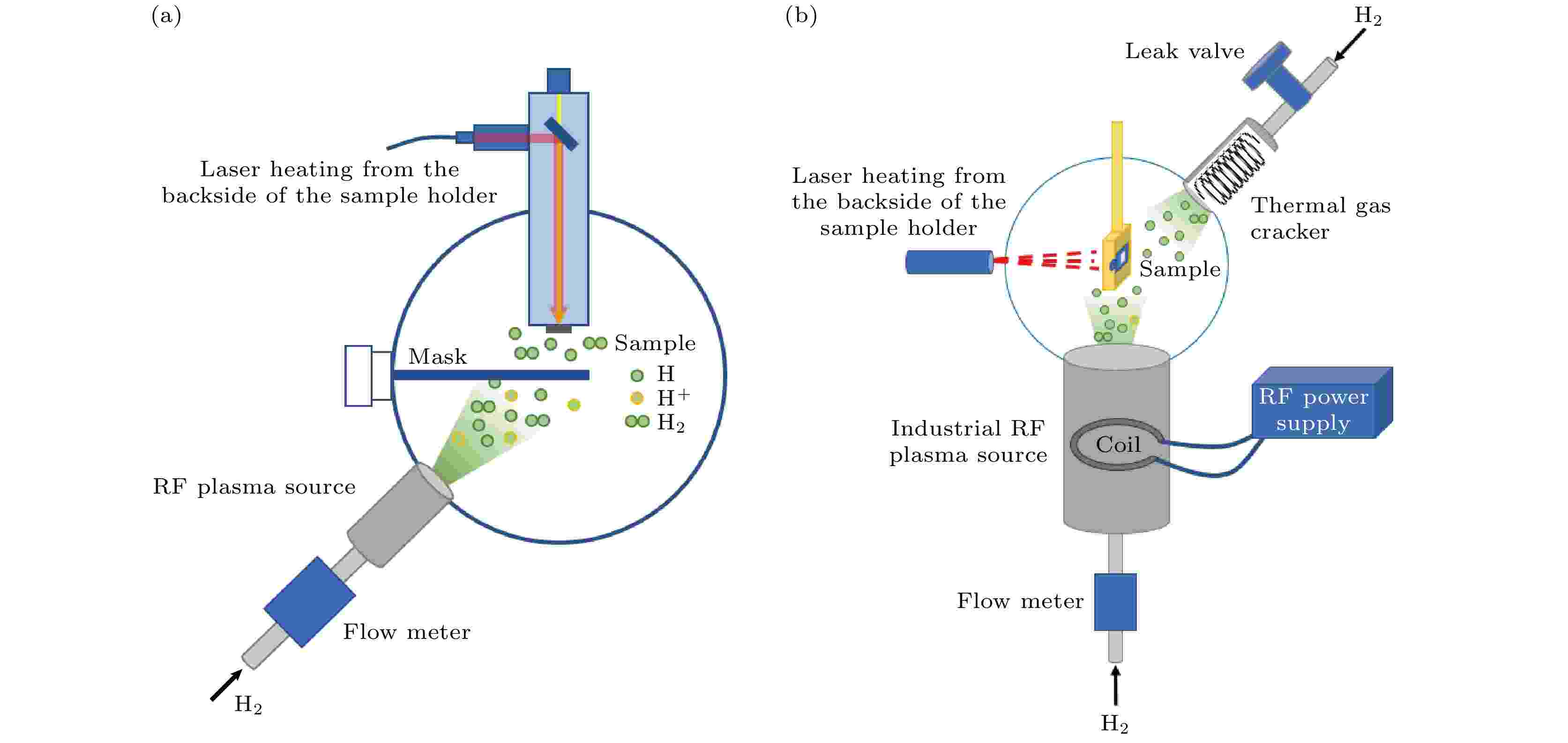
Infinite-layer nickelates, obtained by removing the apical oxygen from perovskite precursors, are the first nickelate system to exhibit superconductivity and provide a platform for exploring unconventional superconductivity. Although the traditional CaH2 sealed-tube reduction method is simple and effective, it is an ex-situ process that tends to cause surface contamination or degradation, making it unsuitable for surface-sensitive measurements like angle resolved photoemission spectroscopy (ARPES). To address this issue, we establish three different in-situ atomic hydrogen reduction methods in an ultrahigh vacuum chamber—namely, a lab-based RF plasma cracker, an industrial RF plasma cracker, and a thermal gas cracker. The key parameters including hydrogen flow, RF power or filament temperature, reduction temperature, and timeare comprehensively optimized using each of the above methods. Structural evolution is monitored by X-ray diffraction (XRD), surface morphology is characterized by atomic force microscopy (AFM), and superconducting properties are examined through electrical transport measurements. The results show that all three in-situ methods can achieve reduction and superconducting properties comparable to or better than CaH2 reduction. Moreover, all atomic hydrogen approaches yield lower surface roughness than CaH2 from the same precursor, highlighting their clear advantage in enhancing surface flatness. Notably, the industrial RF plasma source, due to its higher hydrogen production efficiency, enables sufficient reduction under milder conditions, resulting in even smoother surfaces. This study also provides a detailed summary of the parameter optimization for each method, providing valuable guidance for the controlled reduction of high-quality infinite-layer nickelate thin films.

SPECIAL TOPIC—2D materials and future information devices
EDITOR'S SUGGESTION
2025, 74 (22): 228503.
doi: 10.7498/aps.74.20251115
Abstract +
The increasing demands for high-speed imaging, aerospace, and optical communication have driven in-depth research on broadband photodetectors with high sensitivity and fast response. Two-dimensional (2D) materials have atomic-scale thickness, tunable bandgaps, and excellent carrier transport properties, making them ideal candidates for next-generation optoelectronics. However, their limited light absorption and intrinsic recombination losses remain key challenges. This paper provides an overview of recent progress of 2D-material-based broadband photodetectors. First, the fundamental optoelectronic properties of 2D materials, including bandgap modulation, carrier dynamics, and light–matter interactions, are discussed to clarify their broadband detection potential. Representative material systems, such as narrow-band gap semiconductors, 2D topological materials, and perovskites, are summarized, showing the detection ability from the ultraviolet to the mid-infrared regions. To overcome intrinsic limitations, four optimization strategies are highlighted: heterostructure engineering for efficient charge separation and extended spectral response; defect engineering to introduce mid-gap states and enhance sub-bandgap absorption; optical field enhancement through plasmonic nanostructures and optical cavities to improve responsivity; strain engineering for reversible band structure tuning, particularly suited for flexible devices. These strategies have achieved significant improvements in responsivity, detectivity, and bandwidth, with some devices implementing ultrabroadband detection and multifunctionality. In summary, 2D materials and their hybrids have shown great potential in broadband photodetection, with progress made in material innovation and device architecture optimization. The reviewed strategies, including heterostructure integration, defect modulation, optical field enhancement, and strain engineering, collectively demonstrate the different ways of overcoming intrinsic limitations and improving device performance. Looking ahead to the future, the reasonable combination of these methods is expected to further expand the detection window, improve sensitivity, and achieve multifunctional operations, thereby paving the way for the multifunctional applications of the next-generation broadband photodetectors in imaging, sensing, and optoelectronic systems.
SPECIAL TOPIC—2D materials and future information devices
EDITOR'S SUGGESTION
2025, 74 (22): 228501.
doi: 10.7498/aps.74.20251093
Abstract +
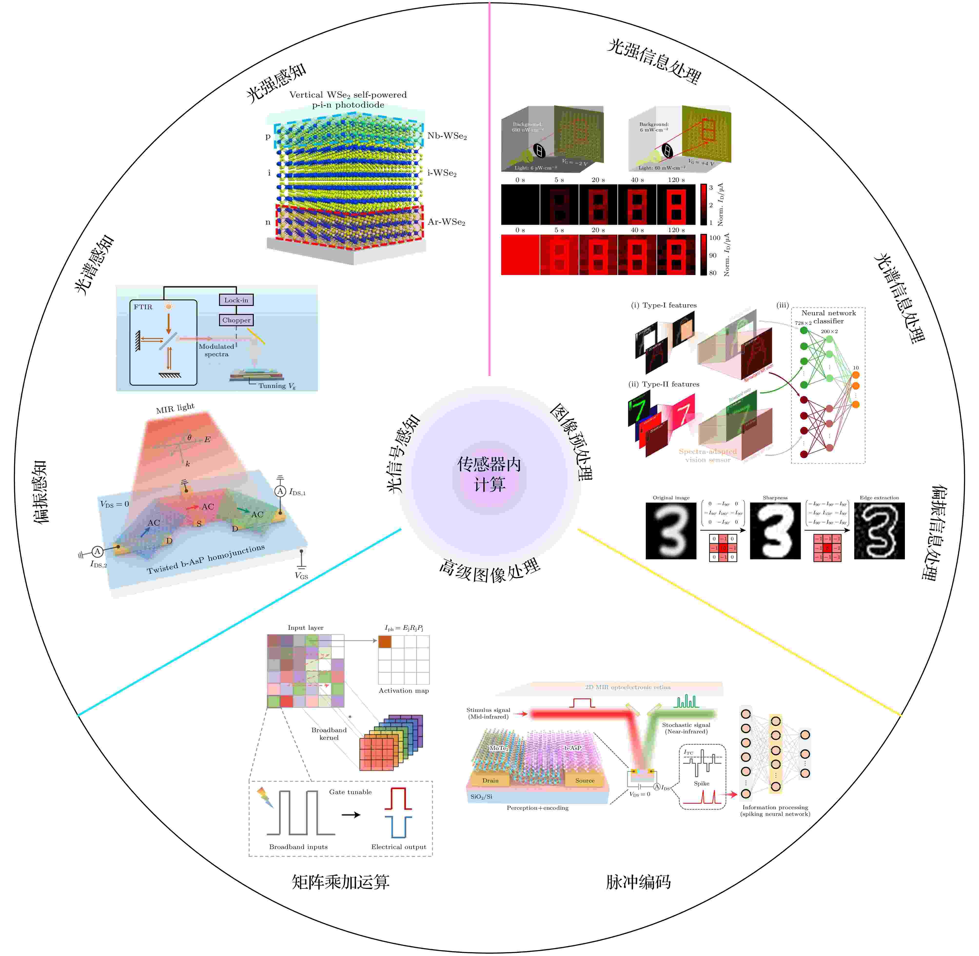
This paper provides a comprehensive review of recent advances in high-performance photodetectors based on two-dimensional materials and in-sensor computing for intelligent image processing, aiming to address the challenges of the “memory wall” and “power wall” caused by the separation of sensing, storage, and computing in traditional image sensors. Traditional image processing relies on the von Neumann architecture, where a large volume of raw data generated at the sensing end must be transmitted to independent computing units or cloud platforms for processing, leading to high energy consumption, significant latency, bandwidth burden, and security risks. Owing to their atomic thickness, high carrier mobility, weak short-channel effects, and tunable optoelectronic properties, two-dimensional (2D) materials provide an ideal physical foundation for achieving function integration of perception and computation. This paper discusses the topic from three perspectives: optical signal perception, image preprocessing, and advanced image processing. In terms of optical signal perception, 2D materials and their heterostructures exhibit ultrahigh responsivity, broadband operation, and fast response in light-intensity detection, enable miniaturized spectrometers through bandgap modulation and computational spectroscopy, and achieve compact, full-polarization analysis via twisted layers and metasurface structures. In image preprocessing, 2D material devices can perform convolution and feature extraction at the sensing end through linear photoresponse, suppress noise and extend dynamic range via superlinear and sublinear responses, and mimic biological visual adaptation in spectral and polarization domains to enhance image quality and robustness. In advanced image processing, the tunable photoresponse and memristive characteristics of 2D materials enable sensor-level integration of sensing, storage, and computation, This allows for the realization of matrix-vector multiplication and convolution operations within convolutional neural networks, significantly reducing power consumption and improving efficiency. Meanwhile, by implementing spike-rate and temporal encoding of optical signals in spiking neural networks, 2D material devices can achieve event-driven image recognition and classification under low-power and low-latency conditions. Furthermore, this paper highlights the challenges faced by 2D material image sensors, including scalable fabrication, heterogeneous integration with silicon technology, array- and circuit-level optimization, environmental stability and encapsulation, and system-level implementation, while envisioning their broad application prospects in intelligent imaging, wearable electronics, autonomous driving, and biomedical diagnostics. It is concluded that with the joint progress in materials science, device engineering, and artificial intelligence, 2D materials are expected to drive the development of next-generation low-power, high-performance, intelligent image processing platforms, and to become an essential foundation for future information perception and processing technologies.
SPECIAL TOPIC—2D materials and future information devices
EDITOR'S SUGGESTION
2025, 74 (22): 227501.
doi: 10.7498/aps.74.20251177
Abstract +
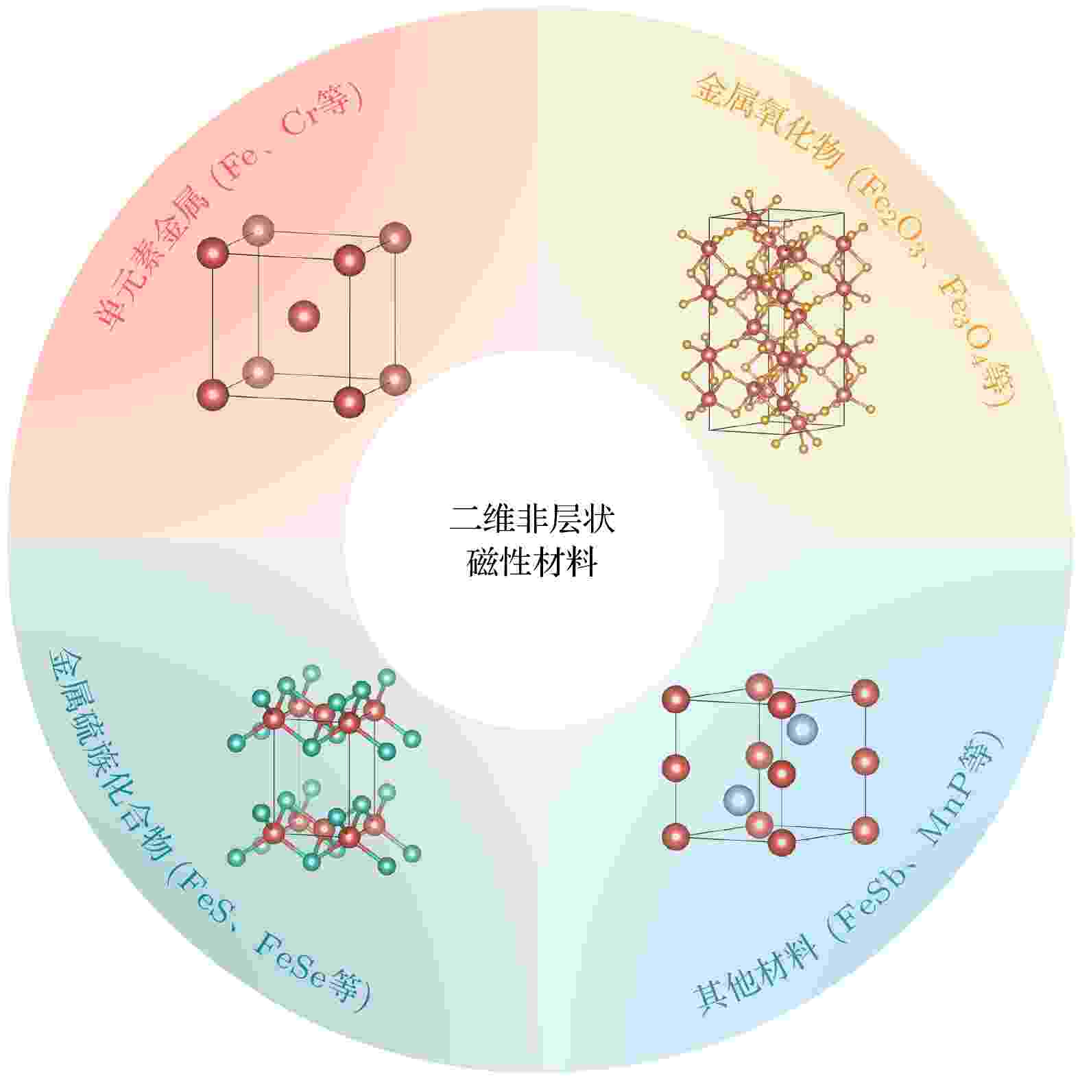
Two-dimensional (2D) magnetic materials refer to nanomaterials with an extremely thin thickness that can maintain long-range magnetic order. These materials exhibit significant magnetic anisotropy, and due to the quantum confinement effect and high specific surface area, their electronic band structures and surface states undergo remarkable changes. As a result, they possess rich and tunable magnetic properties, showing great application potential in the field of spintronics. The 2D magnetic materials include layered materials, where layers are stacked by weak van der Waals forces, and non-layered materials, which are bonded via chemical bonds in all three-dimensional directions. Currently, most of researches focus on 2D layered materials, but their Curie temperatures are generally much lower than room temperature, and they are always unstable when exposed to air. In contrast, the non-layered structure enhances the structural stability of the materials, and the abundant surface dangling bonds increase the possibility of modifying their physical properties. Such materials are attracting increasing attention, and significant progress has been made in their synthesis and applications. This review first systematically summarizes various preparation methods for 2D non-layered magnetic materials, including but not limited to ultrasound-assisted exfoliation, molecular beam epitaxy, and chemical vapor deposition. Meanwhile, it systematically reviews the 2D non-layered intrinsic magnetic materials obtained in various types of materials in the past five years, as well as a series of novel physical phenomena emerging under the ultrathin limit, such as thickness-dependent magnetic reconstruction dominated by quantum confinement effects and planar topological spin textures induced by 2D structures. Furthermore, it also discusses the critical role played by theoretical calculations in predicting new materials through high-throughput screening, revealing microscopic mechanisms by analyzing magnetic interactions, as well as some important methods of modifying magnetism. Finally, from the perspectives of material preparation, physical mechanisms, device fabrication, and theoretical calculations, the current challenges in the field are summarized, and the application potential and development directions of 2D non-layered magnetic materials in spintronic devices are prospected. This review aims to provide comprehensive references and scientific perspective for researchers engaged in this field, thereby promoting further exploration of the novel magnetic properties of 2D non-layered magnetic materials and their applications in spintronic devices.
SPECIAL TOPIC—2D materials and future information devices
EDITOR'S SUGGESTION
2025, 74 (22): 228101.
doi: 10.7498/aps.74.20251305
Abstract +
SPECIAL TOPIC—2D materials and future information devices
EDITOR'S SUGGESTION
2025, 74 (22): 226401.
doi: 10.7498/aps.74.20251141
Abstract +
SPECIAL TOPIC—2D materials and future information devices
EDITOR'S SUGGESTION
2025, 74 (22): 228502.
doi: 10.7498/aps.74.20251165
Abstract +
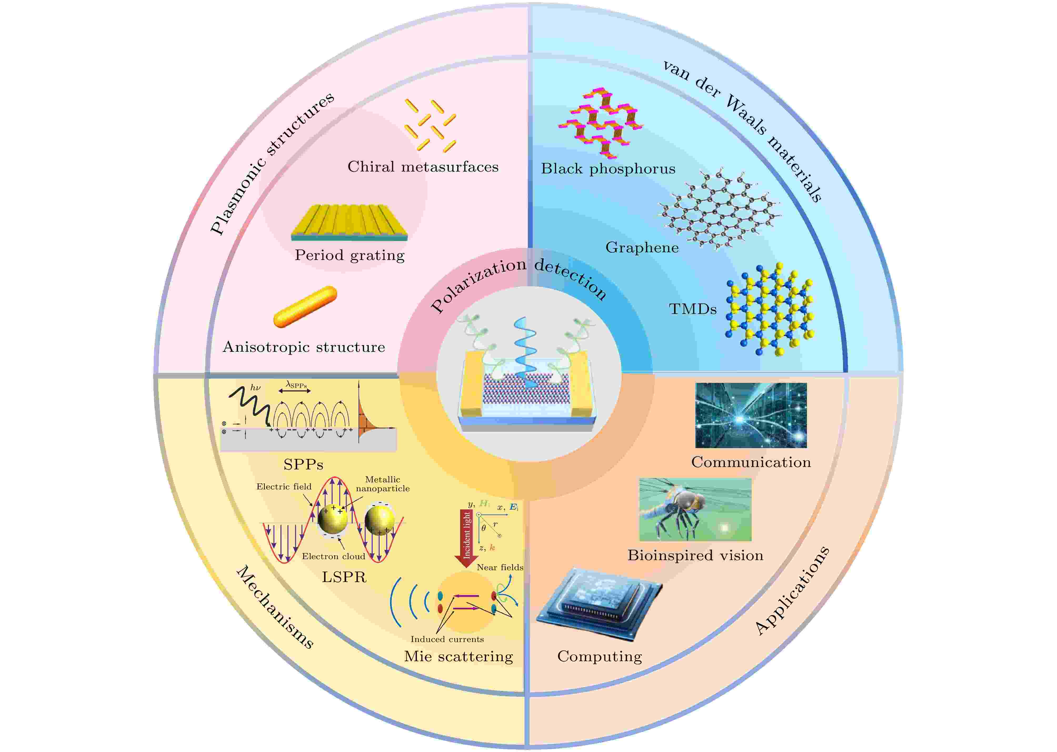
Polarization detection is a fundamental way to obtain the vectorial nature of light, supporting advanced technologies in the fields of optical communication, intelligent sensing, and biosensing. Two-dimensional van der Waals materials have become a promising platform for high-performance polarization-sensitive photodetectors due to their inherent anisotropy and tunable electronic properties. Nevertheless, their intrinsically weak light absorption and limited photoresponse efficiency remain major bottlenecks. Plasmonic nanostructures, which can achieve strong localized field confinement and manipulation on a nanoscale, provide an effective strategy to overcome these limitations and substantially improve device performance. In this review, we systematically summarize the coupling mechanisms between plasmonic architectures and vdW materials, highlighting near-field enhancement, plasmon-induced hot-carrier generation, and mode-selective polarization coupling as key physical processes for enhancing photocarrier generation and polarization extinction. Representative devices including metallic gratings, hybrid nanoantennas, and chiral metasurfaces are compared in terms of responsivity, detection speed, operating bandwidth, and polarization extinction ratio, revealing consistent improvements of one to two orders of magnitude over bare vdW devices. We further survey emerging applications in the fields of high-speed polarization-encoded optical communication, on-chip optical computing and information processing, and bioinspired vision and image recognition systems, where plasmonic-vdW hybrid detectors demonstrate unique advantages in miniaturization and energy efficiency. Finally, we discuss current challenges such as large-scale fabrication of uniform plasmonic arrays, spectral bandwidth broadening, and seamless integration with complementary photonic circuits, and outline future opportunities for next-generation polarization-resolved optoelectronic platforms.

- 1
- 2
- 3
- 4
- 5
- ...
- 211
- 212


