


Vol. 74, No. 24 (2025)
2025-12-20
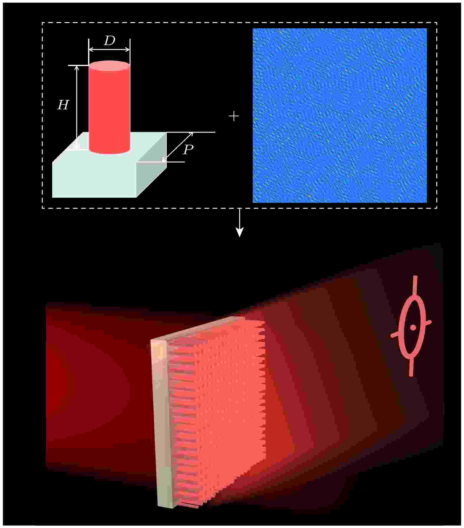
SPECIAL TOPIC—Principles and applications of quantum optics·COVER ARTICLE
COVER ARTICLE
SPECIAL TOPIC—Principles and applications of quantum optics·COVER ARTICLE
COVER ARTICLE
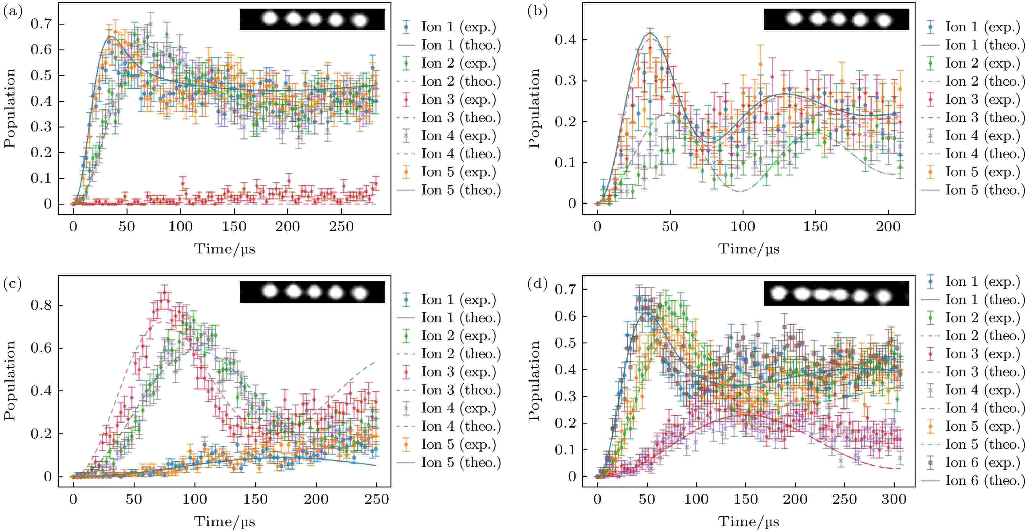
2025, 74 (24): 240301.
doi: 10.7498/aps.74.20251454
Abstract +

SPECIAL TOPIC—AI + Physical Science
EDITOR'S SUGGESTION
2025, 74 (24): 240701.
doi: 10.7498/aps.74.20250989
Abstract +
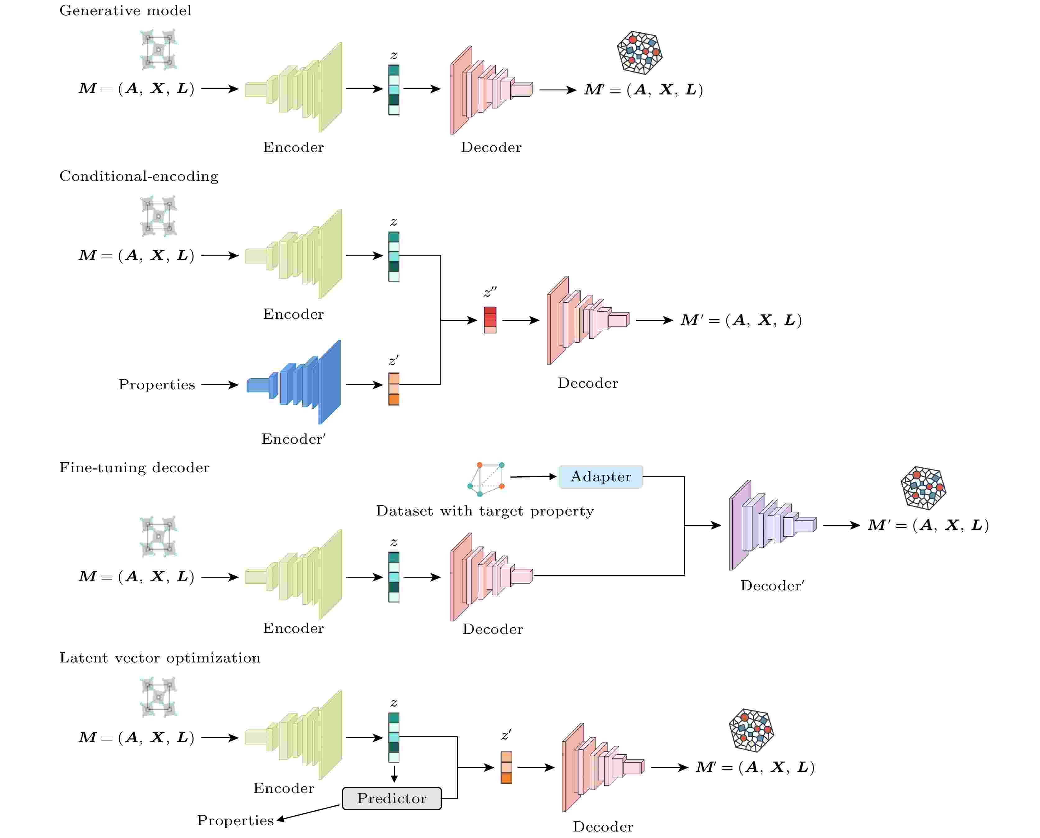
In recent years, the application of machine learning in materials science has significantly accelerated the discovery of new materials. In particular, when combined with traditional methods such as first-principles calculations, machine learning models have proven effective in screening potential high-performance materials from existing databases. However, these methods are largely limited by the known chemical spaces, making it difficult to achieve the active design of novel material structures. To overcome this limitation, generative models have become a promising tool for inverse material design, providing new avenues for exploring unknown structures and property spaces. Although existing generative models have achieved initial progress in crystal structure generation, achieving property-guided material generation remains a significant challenge. In this review paper, we first introduce the representative generative models recently applied to materials generation, including CDVAE, MatGAN, and MatterGen, and analyzes their basic abilities and limitations in structural generation. We then focus on strategies for incorporating target properties into generative models to generate the property-guided structure. Specifically, we discuss four representative methods: Con-CDVAE based on target property vectors, SCIGEN with integrated structural constraints and guidance mechanisms, a fine-tuned version of MatterGen leveraging adapter-based property control, and a CDVAE latent space optimization strategy guided by property objectives. Finally, we summarize the key challenges faced by property-guided generative models and provide an outlook on future research directions. This review aims to offer researchers a systematic reference and inspiration for advancing property-driven generative approaches in material design and provides researchers with a systematic reference and insight into the advancement of property-driven generative methods for materials design.
SPECIAL TOPIC—Semiconductor physics and devices
EDITOR'S SUGGESTION
2025, 74 (24): 241302.
doi: 10.7498/aps.74.20251120
Abstract +
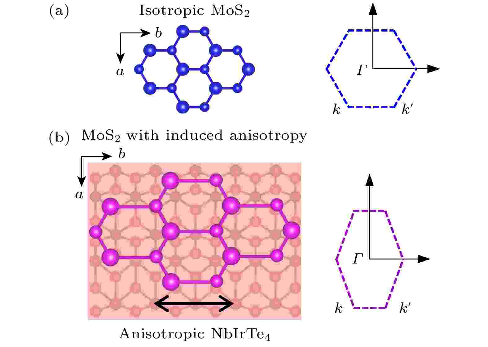
Luminescence and anisotropy in two-dimensional (2D) materials have important implications for both fundamental material physics and potential applications such as polarized light-emitting devices. However, many natural-occuring 2D materials typically exhibit either luminescence or anisotropy, but not both. In this work, we utilize van der Waals (vdW) engineering to construct a heterostructure (HS) with anisotropic luminescent properties, which is composed of isotropic monolayer (1L) MoS2 (with strong intrinsic luminescence) and low-symmetry NbIrTe4 (strong anisotropy without photoluminescence). Experimentally, we characterize the optical response of the HS by using angle-resolved PL spectroscopy. The results indicate that the intrinsic anisotropic potential field of NbIrTe4 at the interface effectively breaks the in-plane isotropic symmetry of MoS2, inducing a pronounced polarization-dependent emission of A and B excitons. The anisotropy ratio is enhanced to ~1.58, corresponding to a linear polarization degree of approximately 22%. This work provides new insights into 2D interfacial coupling and offers useful guidance for the design and engineering of next-generation high-performance, tunable polarized light-emitting devices.
SPECIAL TOPIC—Instrumentation and metrology for ultrafast atomic and molecular spectroscopy
EDITOR'S SUGGESTION
2025, 74 (24): 243202.
doi: 10.7498/aps.74.20251166
Abstract +
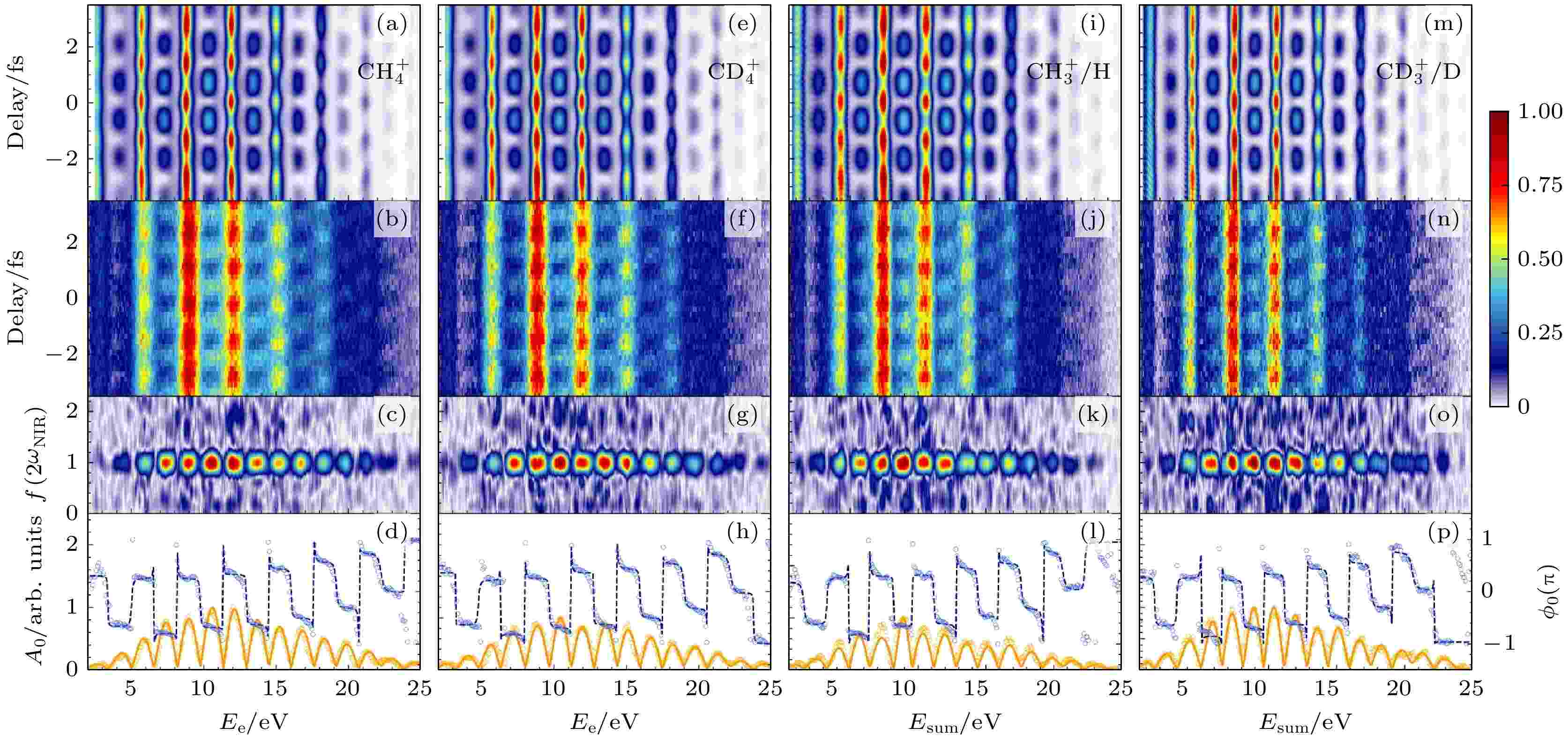
The evolution mechanisms of electrons in isolated atoms, molecules and complex systems on a natural time-scale have long been a fundamental question in atomic and molecular physics, with significant implications for the applications of quantum materials. Over the past two decades, the development of attosecond light pulses and attosecond metrology has opened new opportunities for investigating the electronic dynamics, while also posing new challenges. Traditional detection techniques, such as time-of-flight and velocity map imaging spectrometers, can be used to study the attosecond scattering phase shifts in the photoemission and ionization processes with extremely high temporal and energy resolution. However, the limitations in multi-particle coincidence detection and three-dimensional momentum correlation limit the deeper exploration of many-body correlations and non-adiabatic ultrafast dynamics involving electron-nuclear coupling. To enable multidimensional and real-time observation of the three-dimensional momenta of both electrons and ions during photoionization, the attosecond interferometry has been integrated into electron-ion coincidence systems. In this study, we utilize an attosecond coincidence interferometer that combines an attosecond pump-infrared femtosecond probe scheme with cold target recoil ion momentum spectroscopy. The apparatus enables attosecond-time-resolved momentum imaging of all charged fragments in atomic and molecular systems, thereby providing deeper insights into the dynamics of photoionization. We also highlight the recent groundbreaking applications and advances of attosecond coincidence interferometer in studying photoionization dynamics in atoms, molecules, and more complex systems.
EDITOR'S SUGGESTION
2025, 74 (24): 244204.
doi: 10.7498/aps.74.20251130
Abstract +
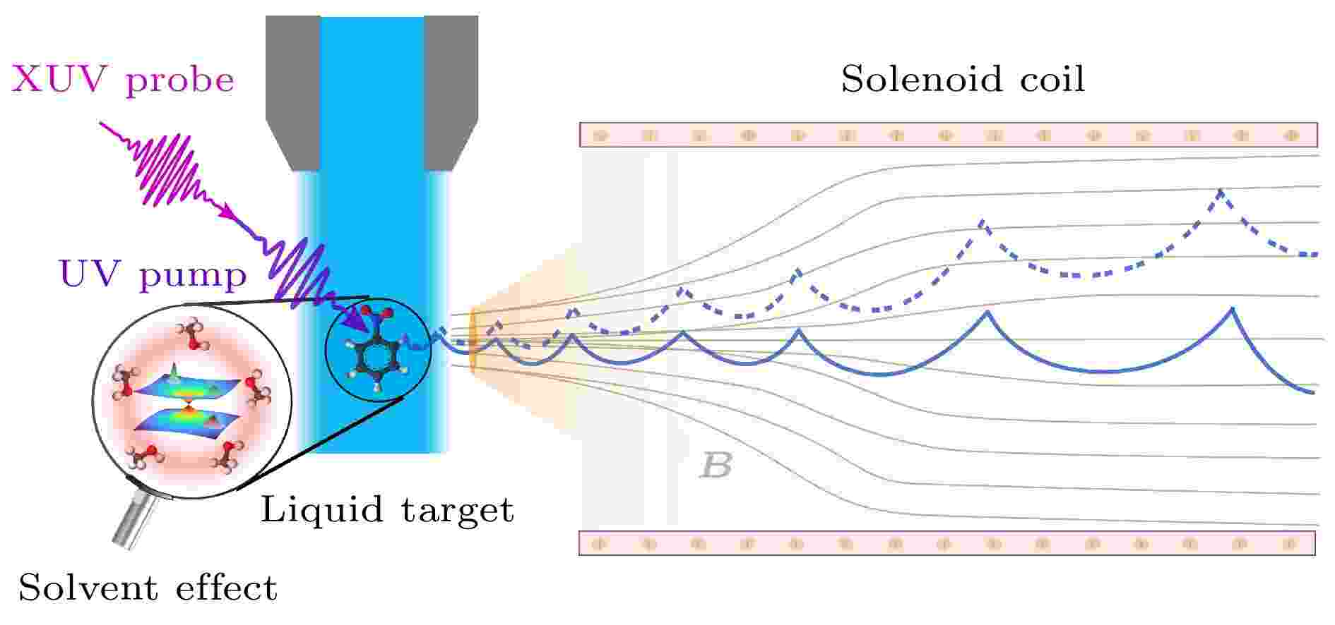
The liquid phase serves as a critical environment for chemical and biological reactions. The chemical and biological reaction dynamics of molecules in liquids exhibit evolution behaviors that are significantly different from those of isolated molecules in the gas phase. The in-depth investigation of the ultrafast excited-state dynamics of liquid-phase molecules is of great importance for uncovering the microscopic mechanisms underlying complex chemical and biological processes. Photoelectron spectroscopy not only reveals the electronic structure of excited-state molecules but also exhibits high sensitivity to structural changes, making it a powerful tool for studying the relaxation dynamics. Liquid-phase time-resolved photoelectron spectroscopy utilizes a liquid microjet within a high vacuum. In this pump-probe technique, an initial pump pulse excites the liquids to initiate dynamics, followed by a delayed probe pulse that ionizes the evolving system. The time-dependent energy distribution of the resulting photoelectrons, which encodes the ultrafast dynamics, is measured by a magnetic-bottle time-of-flight (MB-TOF) analyzer. This review systematically summarizes recent advancements in the time-resolved liquid-phase photoelectron spectroscopy technology for studying ultrafast dynamics in liquids, detailing the fundamental working principles of magnetic-bottle spectrometers and the preparation techniques for liquid microjet targets. Furthermore, typical applications are discussed, concluding with an analysis of current technical challenges and future research directions.
EDITOR'S SUGGESTION
2025, 74 (24): 243203.
doi: 10.7498/aps.74.20251176
Abstract +
SPECIAL TOPIC—Atomic, molecular and materials properties data
EDITOR'S SUGGESTION
2025, 74 (24): 243101.
doi: 10.7498/aps.74.20251230
Abstract +
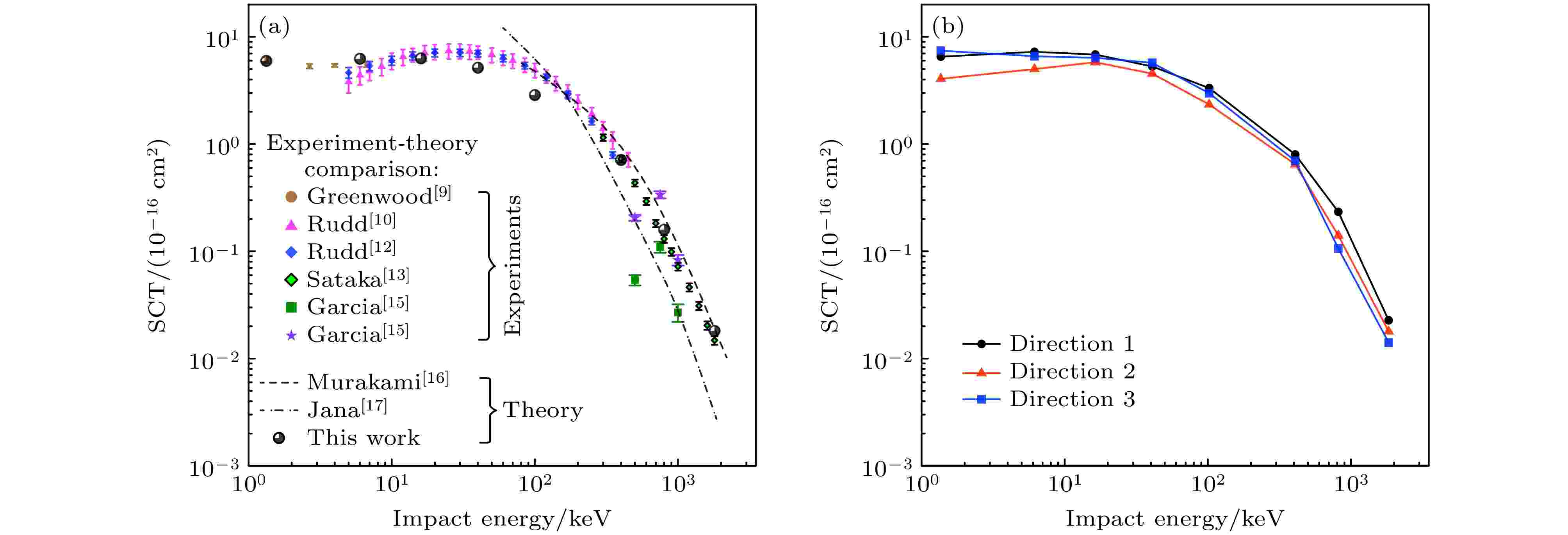
The charge transfer cross sections of collisions between He ions in the solar wind and H2O molecule constitute essential data required for the astrophysical plasma modeling. However, experimental measurements of single charge transfer (SCT) cross sections for He+-H2O collisions at low-to-intermediate energies (corresponding to the velocity range of the solar wind) are extremely scarce, and first-priciple theoretical calculations have not been conducted. In this study, employing the time-dependent density functional theory nonadiabatically coupled with the molecular dynamics, the SCT cross sections are calculated for He+-H2O collisions over a broad energy range of 1.33–1800 keV. An inverse collision framework is used to investigate the charge transfer dynamics and electron-ion coupling processes. It is found that the SCT cross section exhibits a strong dependence on the molecular orientation. Furthermore, there are significant differences in the contributions of different molecular orientations to the cross section between low-energy and high-energy regions. The computed cross section results show good agreement with the existing data obtained from experiments and classical theoretical models. This indicates that the present theoretical method and numerical framework are not only applicable to handling the charge transfer processes in collisions between dressed ions and molecules but also enable the quantitative analysis of the effect of molecular orientation on the cross section. This study lays a foundation for cross section calculations of complex collision systems. The datasets presented in this paper are openly available at https://doi.org/10.57760/sciencedb.j00213.00193 .
EDITOR'S SUGGESTION
2025, 74 (24): 245101.
doi: 10.7498/aps.74.20250861
Abstract +
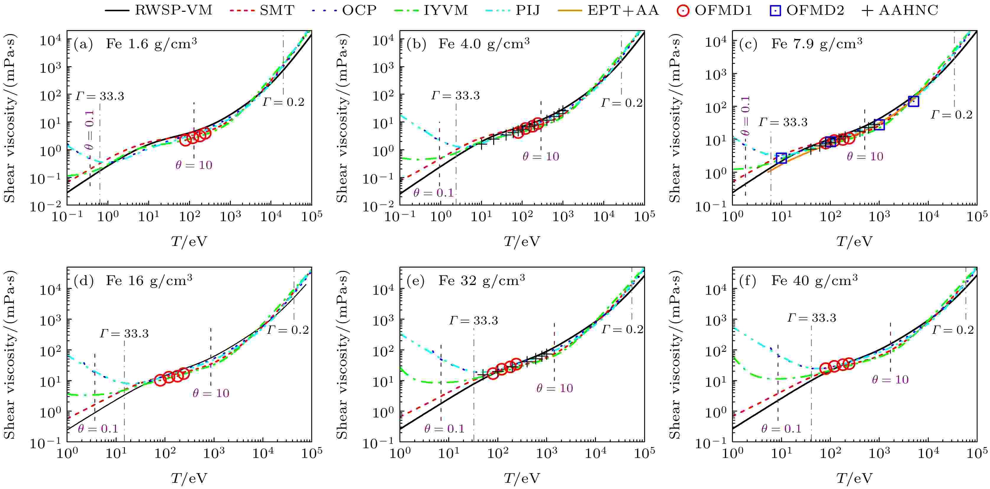
The viscosities of matters under extreme conditions, i.e. warm dense matter (WDM) and hot dense matter (HDM), have significant applications in various fields, such as the design of inertial confinement fusion targets, the astrophysical structure evolution, and the interfacial instability and mixing development under extreme conditions. Since the temperature and pressure ranges accessible by experimental techniques for viscosity measurement are very limited, the acquisition of viscosity data under extreme conditions mainly relies on theoretical calculations. This work introduces a variety of molecular dynamics (MD) methods and models for calculating the viscosities of WDM and HDM, they being quantum MD (QMD), orbital-free MD (OFMD), average atom model combined with hypernetted chain (AAHNC), effective potential theory combined with average atom model (EPT+AA), hybrid kinetics MD (KMD), integrated Yukawa viscosity model (IYVM), Stanton-Murillo transport model (SMT), pseudo-ion in jellium (PIJ), one-component plasma model (OCP), and random-walk shielding-potential viscosity model (RWSP-VM). Simultaneously, the viscosities of various elements obtained by these methods are shown, ranging from low to high atomic number (Z), i.e., H, C, Al, Fe, Ge, W, and U. The accuracy and the applicability of each method are analyzed in detail by comparison. RWSP-VM, which is based on physical modeling and independent of MD data, has comparable accuracy to simulation data over a wide range of temperature and pressure, and is an efficient method of obtaining viscosity data of WDM and HDM. This work will pave the way for calculating the shear viscosities under extreme conditions, and may play an important role in promoting the relevant applications. The data calculated from RWSP-VM in this work are openly available at https://doi.org/10.57760/sciencedb.j00213.00180 .
EDITOR'S SUGGESTION
2025, 74 (24): 246201.
doi: 10.7498/aps.74.20251058
Abstract +
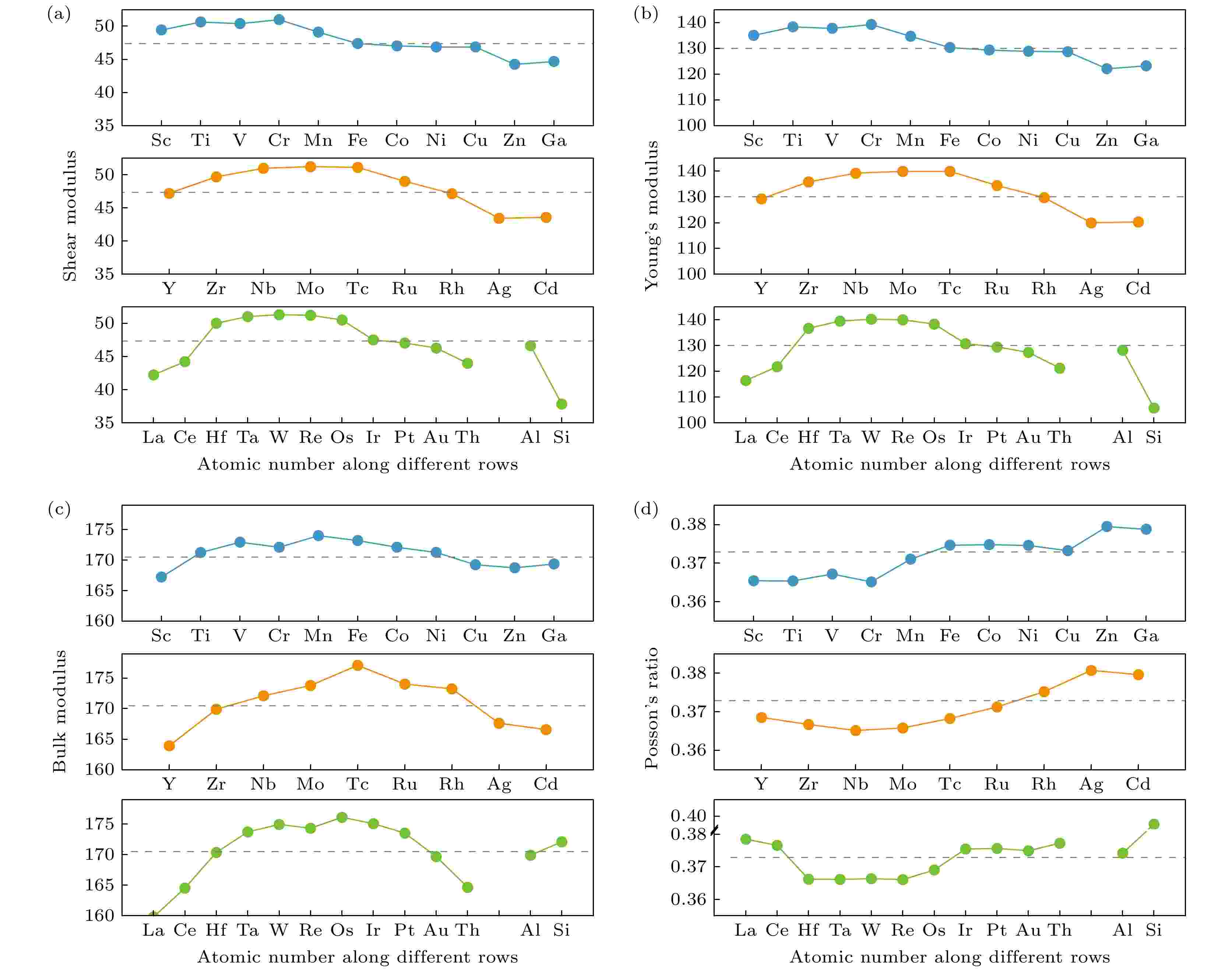
The lower friction coefficient and superior mechanical properties of palladium (Pd) alloys make them potentially advantageous for use in high-precision instruments and devices that require long-term stable performance. However, the high cost of raw materials and experimental expenses result in a lack of fundamental data, which hinders the design of high-performance Pd alloys. Therefore, in this study, first-principles calculations are used to determine the lattice constant and elastic modulus of Pd. A model of dilute solid solutions formed by Pd with 33 alloying elements including Al, Si, Sc, Ti, V, Cr, Mn, Fe, Co, Ni, and others, is established. The mixing enthalpy, elastic constant, and elastic modulus are calculated. The results show that, all other alloying elements except for Mn, Fe, Co, Ni, Ru, Rh, Os, and Ir can form solid solutions with Pd. Alloying elements from both sides of the periodic table enhance the ductility of Pd solid solutions, with La, Ag, and Zn having the most significant effects, while Cu and Hf reduce the ductility of Pd. Differential charge density analysis indicates that the electron cloud formed after doping with Ag is spherically distributed, thereby improving ductility. After doping with Hf, the degree of delocalization around the atoms is maximized, indicating a strong ionic bond between Hf and Pd, which results in a higher hardness of Pd31Hf. The datasets presented in this paper are openly available at https://www.doi.org/10.57760/sciencedb.j00213.00186 .
GENERAL
EDITOR'S SUGGESTION
2025, 74 (24): 240201.
doi: 10.7498/aps.74.20251073
Abstract +
Owing to, Solid-state batteries have gradually become the focus of people’s attention and research in recent years due to the advantages of high energy density and high safety factor. Lithium dendrites are a key factor affecting battery safety and service life, and in severe cases, battery short circuits can occur. Compared with liquid batteries, solid-state batteries rely on solid-state electrolytes with higher mechanical strength, which can effectively inhibit the growth of lithium dendrites, but with the increase of the number of charge-discharge cycles, the dead lithium produced by the incomplete dissolution of lithium dendrites gradually accumulates, and the performance of the battery gradually decreases. In this work, the problem of dead lithium in solid-state batteries is studied by using COMSOL Multiphysics 6.2 finite element simulation software. Due to the fact that existing research on dead lithium mainly focuses on phase field models combined with binary physics, there is little research on the influence of electrochemical parameters on dead lithium. Therefore, the phase field method is used to simulate the dissolution of lithium dendrites and the formation of dead lithium under the coupling of force-thermal-electrochemical fields. When the heat transfer model is coupled, the difference in the morphology of dead lithium before and after the coupled heat transfer model is further studied by applying an external pressure to change the stress of lithium dendrites. When the coupled mechanical field changes, the morphology of dead lithium before and after the coupled mechanical field is further studied by changing the temperature magnitude. At the same time, the effects of changes in three electrochemical parameters, namely diffusion coefficient, interfacial mobility and anisotropic strength, on the area of dead lithium are also explored. The research results indicate that when the heat transfer model or mechanical field is coupled into the phase field model, the dendrite dissolution cut-off time and dead lithium area will change. When the base rises at high temperature or when low external pressure or high external pressure is applied, the area of dead lithium decreases. For changing the electrochemical parameters, reducing the diffusion coefficient, increasing the interfacial mobility and reducing the anisotropic strength can effectively reduce the area of dead lithium.
EDITOR'S SUGGESTION
2025, 74 (24): 240501.
doi: 10.7498/aps.74.20251142
Abstract +
2025, 74 (24): 240502.
doi: 10.7498/aps.74.20251102
Abstract +
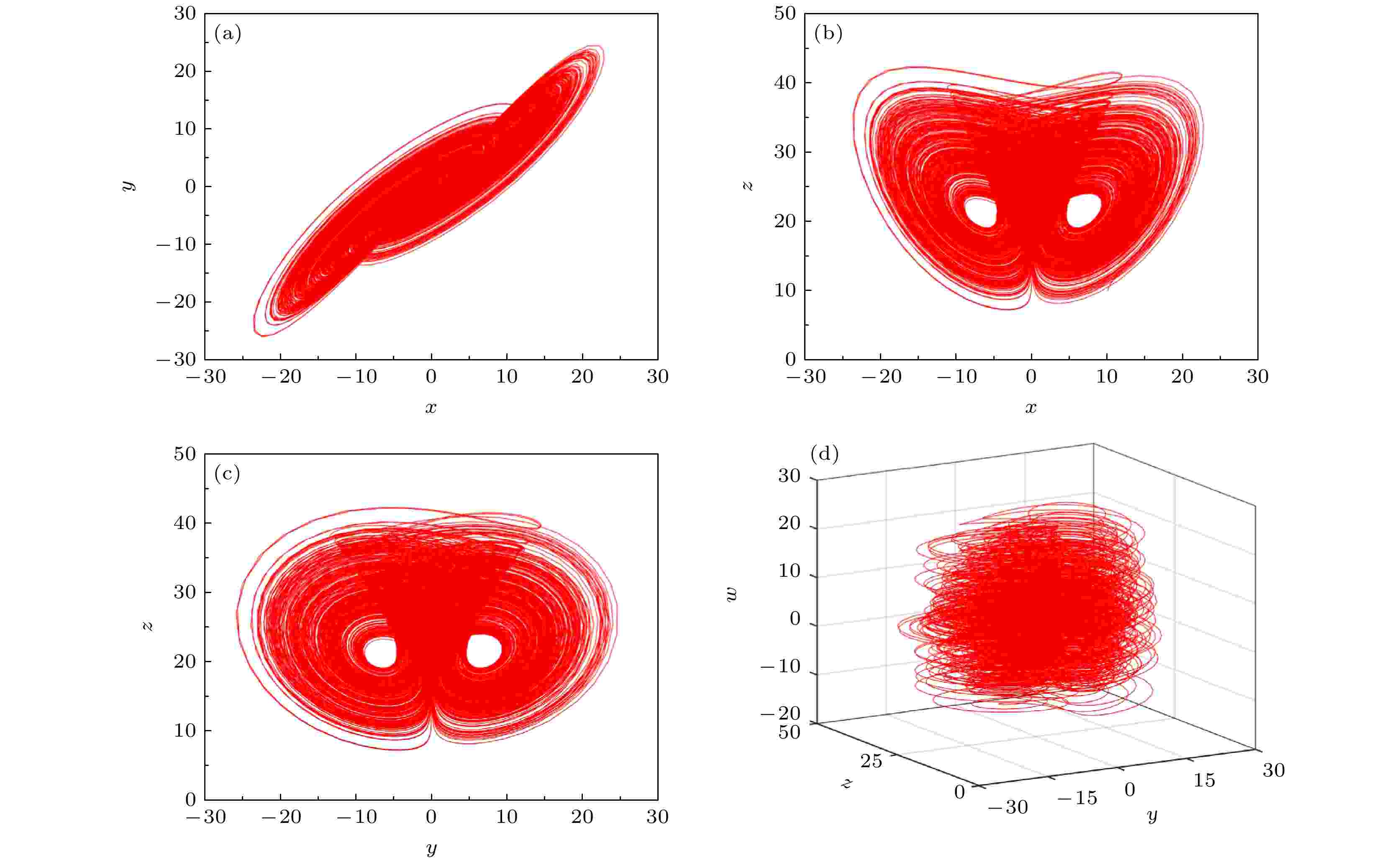
Memristors exhibit controllable nonlinear characteristics, generating chaotic signals that are characterized by randomness, sensitivity, and unpredictability, thereby demonstrating significant potential applications in information encryption and signal processing. With the integration of chaos theory and electronic technology, constructing memristive hyperchaotic systems has become a hot topic in nonlinear science and information security. To overcome the limitation of monotonic dynamic characteristics in traditional chaotic systems, we design a novel memristor-based hyperchaotic system with richer dynamic behavior and higher application value in this paper. Moreover, the characteristic analysis, theoretical verification, application exploration, and hardware implementation are conducted to support the engineering applications of the system. Building upon the classical Chen system, this work is innovatively combined with a cubic nonlinear magnetically controlled memristor model as a feedback element. By establishing a mathematical model of the memristor and coupling it with the state equations of the Chen system, we design a four-dimensional memristor-based hyperchaotic system. First, by integrating numerical computation with differential equation theory, a comprehensive mathematical model is established to analyze fundamental properties, such as symmetry and dissipativity, thereby validating the system’s rationality. Second, the system’s dynamical behaviors are analyzed, including attractor phase diagrams, Lyapunov exponents, power spectra, parameter effects, transient dynamics, and coexisting attractors. Simultaneously, variational methods are utilized to analyze unstable periodic orbits within the system. A symbolic coding approach based on orbital characteristics is established to convert orbital information into symbolic sequences, and orbital pruning rules are explored to provide a basis for optimal orbital control. Furthermore, a digital image encryption method is proposed based on this system. Using chaotic sequences as keys, image pixels are scrambled and diffused. The effectiveness of encryption is validated through histogram analysis, correlation analysis, information entropy evaluation, and testing of anti-attack capabilities. Finally, a DSP-based digital circuit hardware platform is constructed to run the system, and the hardware experimental results are compared with software simulation outcomes. These findings reveal that the introduction of memristors induces linearly distributed equilibrium points in phase space, generating hidden attractors that enrich the chaotic behavior of the system. The simulation of dynamic behavior confirms the rich dynamics of this four-dimensional memristor-based hyperchaotic system. The proposed digital image encryption method demonstrates robust security performance. The DSP hardware experiments and software simulations yield highly consistent attractor phase diagrams, validating the correctness and feasibility of the system.
EDITOR'S SUGGESTION
2025, 74 (24): 240702.
doi: 10.7498/aps.74.20251146
Abstract +
THE PHYSICS OF ELEMENTARY PARTICLES AND FIELDS
EDITOR'S SUGGESTION
2025, 74 (24): 241301.
doi: 10.7498/aps.74.20250639
Abstract +
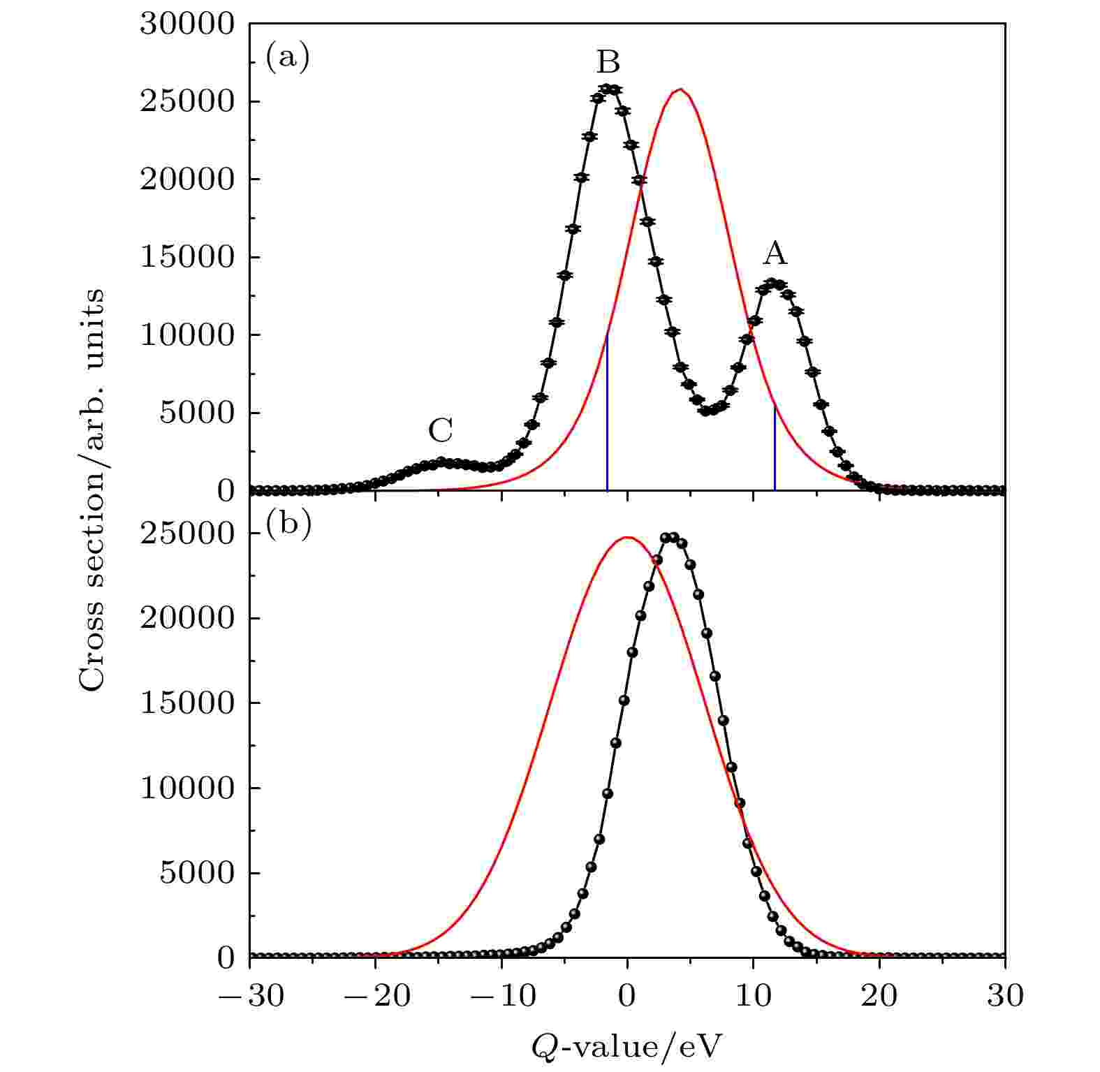
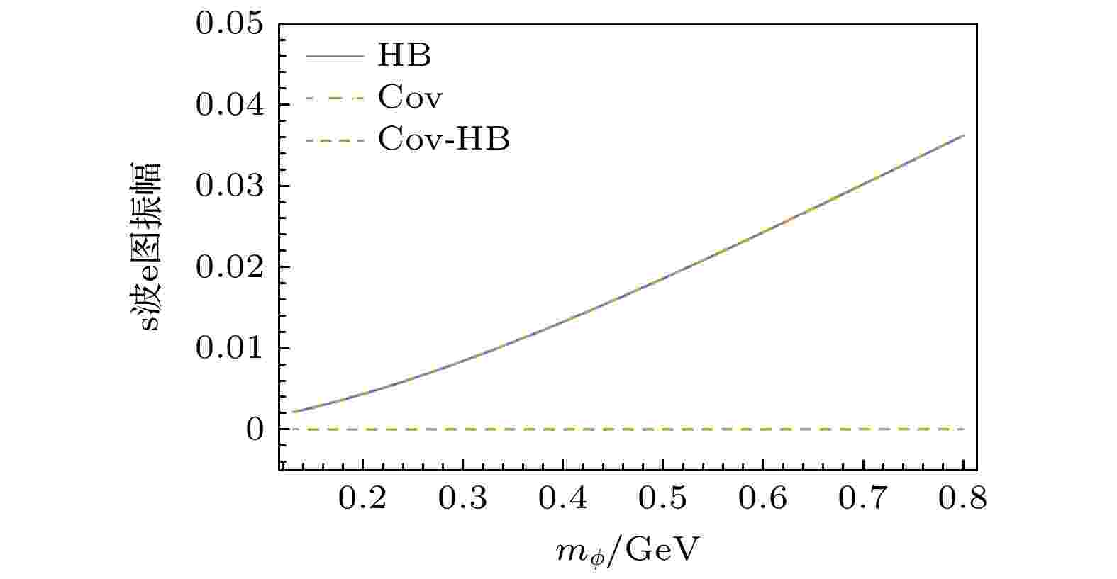
An unresolved issue in the study of baryon non-leptonic decays is that the theoretical values describing the s- and p-wave amplitudes of such decays cannot simultaneously accord well with experimental values. Compared with previous literature, this paper adopts the covariant chiral effective theory framework and calculates the one-loop corrections to the s- and p-wave amplitudes by using the extended minimal subtraction (EMS) scheme, and also takes into account the contributions from intermediate pion states that are neglected in previous studies (the contributions from intermediate decuplet states are not considered here). Unlike infrared regularization and the extended on-shell subtraction scheme, EMS is easier to implement and also avoids over-subtraction. Apart from the typical chiral logarithmic term mslnms obtained in heavy-baryon formalism, the covariant calculation retains many non-local contributions that are not negligible. These non-local contributions vary with loop diagrams and intermediate states, making the complete covariant results significantly different from those from the simple chiral logarithmic structures in heavy-baryon formalism, which may alleviate the tension between the s- and p-wave components of the decay amplitudes. Subsequent numerical analysis confirms this conjecture. Two approaches are adopted to obtain covariant theoretical predictions: s-wave fitting and p-wave fitting. According to the fitted predictions and chi-squares of fitness, the s-wave fitting yields s-wave predictions slightly inferior to those under heavy-baryon formalism, but the resulting p-wave predictions are considerably improved compared with the heavy-baryon formalism predictions. The p-wave fitting produces p-wave predictions closer to experimental values, while the heavy-baryon predictions differ significantly from the experimental values. The resulting s-wave predictions from p-wave fitting show noticeable discrepancies with experimental data, but the heavy-baryon predictions are even worse. Therefore, working in the covariant framework, the tension between s- and p-wave amplitudes for baryon non-leptonic decays is significantly alleviated in comparison with that in heavy-baryon formalism. In addition, it is found that the contributions from intermediate pion states may be neglected in many cases, but are important and must be kept for decays with smaller experimental values.
ATOMIC AND MOLECULAR PHYSICS
2025, 74 (24): 243201.
doi: 10.7498/aps.74.20250677
Abstract +
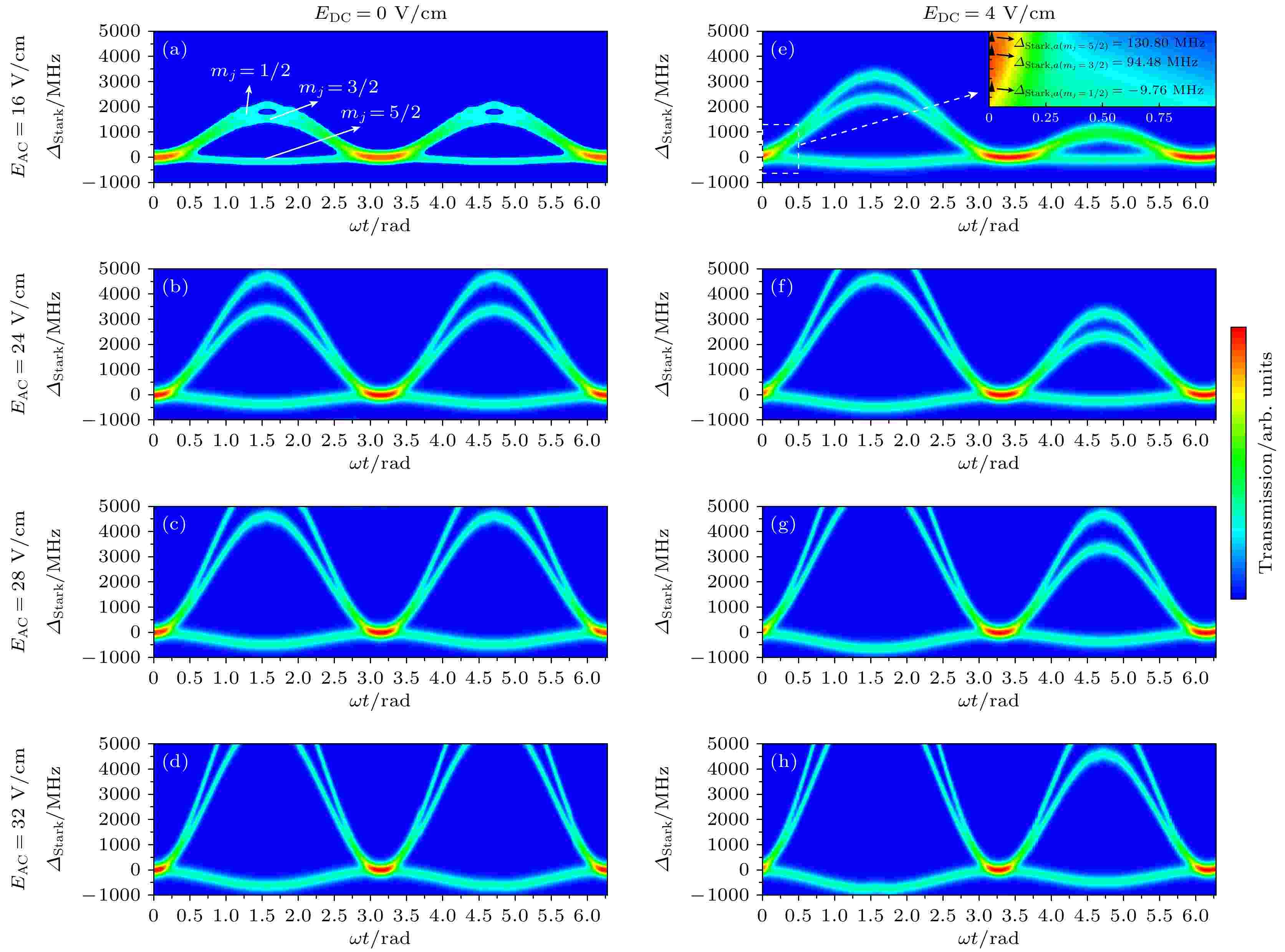
The Stark effect in Rydberg atoms exhibits remarkable sensitivity to external electric fields, thus forming the fundamental basis for precision electric field measurements. This study systematically and comprehensively investigates the regulatory effects of DC and AC electric fields on cesium Rydberg atoms, both experimentally and theoretically. Utilizing a two-photon three-level system, we generate 28D5/2 Rydberg states and establish electromagnetically induced transparency (EIT) as the macroscopic observable. Our experimental results demonstrate distinct Stark splitting patterns under DC fields, revealing three fine-structure states each with polarization-dependent frequency shift, they being the negative polarizability states (mj = 1/2, 3/2) exhibiting rightward shifts, and the positive polarizability state (mj = 5/2) showing leftward displacement. For power-frequency AC fields (50 Hz), we observe characteristic double-frequency modulation of the EIT-Stark spectra, with measurement limitations emerging at field strengths above 24 V/cm due to laser scanning range constraints. To overcome this limitation, we develop an innovative DC field regulated measurement scheme, establishing a dynamic model for the combined AC/DC field interaction with Rydberg atoms. The model successfully derives demodulation expressions for extracting both DC and AC field components from the composite spectral shifts. Experimental validation shows that applying an 8 V/cm DC bias field can extend the measurable AC field range to 32 V/cm, achieving a 33.3% improvement over direct measurement methods within a 1 GHz laser scanning range, while maintaining exceptional accuracy with demodulation errors below 0.8% across all tested configurations. The detailed error analysis reveals that the measurement precision improves with the increase of field strength, with a standard deviation of σ = 0.2196%, demonstrating the robustness of our approach. Compared with existing techniques, this DC-field regulation method effectively addresses the critical challenge of limited laser scanning range in strong-field measurements, while preserving the quantum advantages of Rydberg atom sensors. The research provides both theoretical foundations and practical solutions for measuring power-frequency strong electric fields in power systems, with potential applications extending to other low-frequency strong-field measurement scenarios. Future work will focus on enhancing measurement stability in extreme field conditions, improving accuracy, and further expanding the operational range of this quantum sensing technology.
ELECTROMAGNETISM, OPTICS, ACOUSTICS, HEAT TRANSFER, CLASSICAL MECHANICS, AND FLUID DYNAMICS
2025, 74 (24): 244201.
doi: 10.7498/aps.74.20251068
Abstract +
Metasurface holography based on planar optical devices has attracted considerable attention due to its potential for miniaturizing optical components and systems. However, traditional on-axis holography has inherent zeroth-order diffraction and twin-image effects, which significantly degrade image quality and limit its practical applications. Off-axis metasurface holography, in contrast, provides a promising solution to overcoming these limitations. In this work, we design a metasurface hologram composed of titanium dioxide (TiO2) nanopillars on a silicon dioxide (SiO2) substrate, by using the high refractive index and low optical loss of TiO2 in the visible light range to achieve efficient phase control. The unit cell height is set to 600 nm to ensure sufficient phase accumulation, and the working wavelength is 635 nm. The hologram is constructed by mapping the continuous 0–2π phase distribution obtained from computational holography onto the unit cell array, and changing the nanopillar diameter to achieve full phase coverage. We systematically investigate the effect of the unit cell period on the imaging position in off-axis holography. Numerical simulations show that as the period increases from 280 nm to 350 nm, the center of the holographic image gradually shifts toward the center of the image plane. The optimal period is found to be 324 nm, at which the image is reconstructed precisely at the designed position. Further simulations using different off-axis angles (0°–45°) and nanopillar heights (600–2000 nm) confirm that the imaging position remains fixed at the target location, indicating that it is mainly determined by the unit cell period rather than other structural parameters. These results demonstrate that by carefully selecting the unit cell period, the holographic image can be accurately reconstructed at a predetermined positions with high image quality, providing theoretical guidance for designing high-precision off-axis metasurface holographic imaging systems.
2025, 74 (24): 244202.
doi: 10.7498/aps.74.20251033
Abstract +
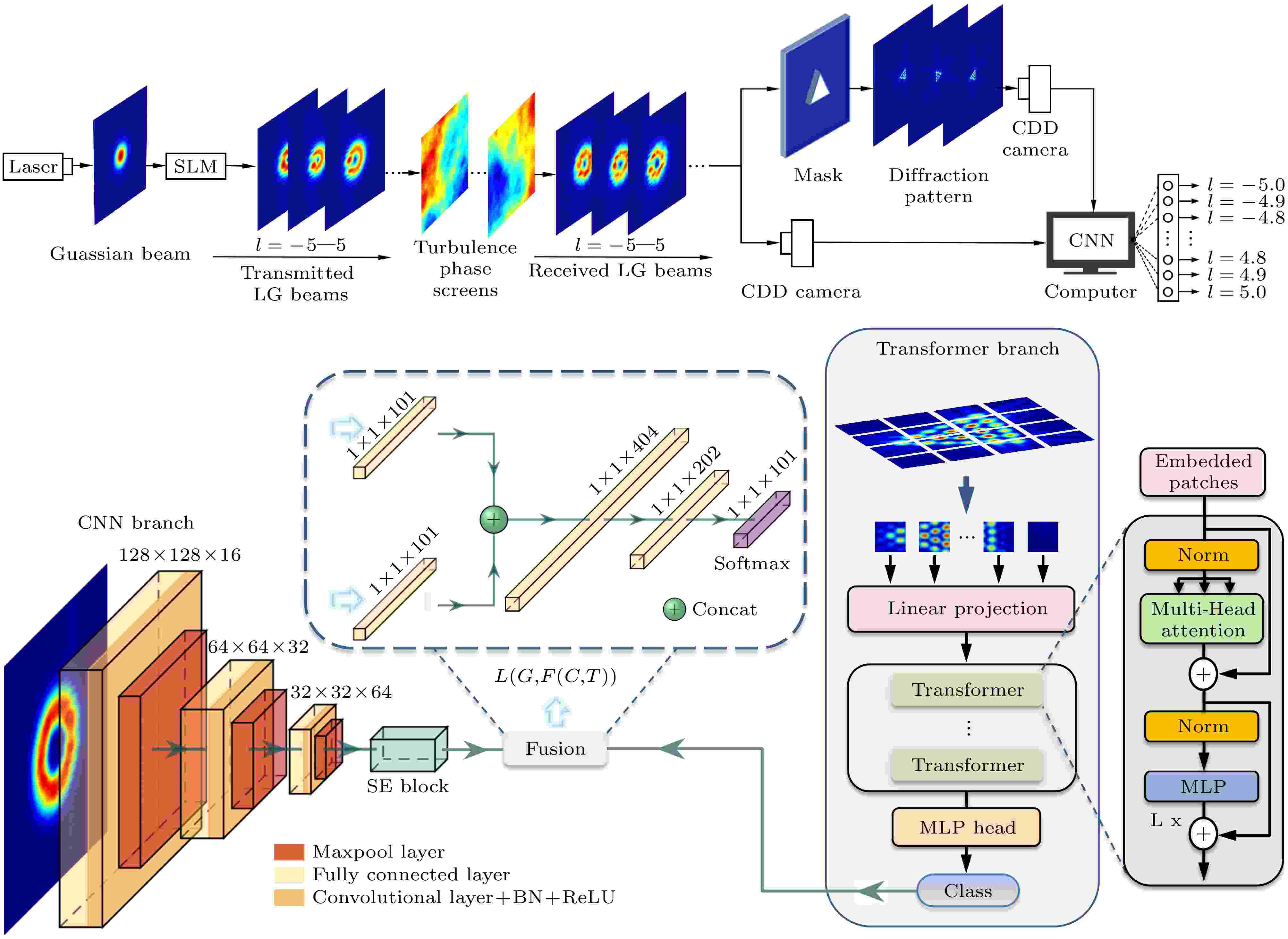
Utilizing fractional vortex beams (FVBs) as information carriers can significantly enhance the capacity of communication systems. However, the small gap difference between adjacent fractional orbital angular momentum (FOAM) modes makes FVBs highly sensitive to atmospheric turbulence. Therefore, precise measurement of distorted FOAM modes is crucial for practical FVBs-based communication systems. To fully utilize the beam intensity information and the triangular diffraction pattern information, we propose a dual-channel deep learning model with a hybrid architecture combining convolutional neural network (CNN) and vision transformer (ViT). The beam intensity information is extracted using the CNN, while the diffraction pattern information is extracted using the ViT. Then, by combining the complementary feature information from the intensity distribution of FVBs and their triangular diffraction patterns, this model can effectively identify the FOAM modes. The results show that the proposed model only requires a relatively small number of samples to reach convergence, namely 100 sets of data under weak turbulence and 400 sets of data under strong turbulence. Moreover, within a transmission distance of 1000 m, the proposed model can identify 101 FOAM modes with a mode spacing of 0.1 with an accuracy of 100% under weak and moderate turbulences, and maintains 98.12% accuracy under strong turbulence. Furthermore, the model can expand the detection range of turbulence intensity with only a minimal loss in accuracy, exhibiting strong generalization ability under unknown atmospheric turbulence strengths, thus providing a novel approach for accurately identifying FOAM modes.
2025, 74 (24): 244203.
doi: 10.7498/aps.74.20251124
Abstract +
Gold nanorods (AuNRs) have become highly promising biomedical probes due to their tunable plasmonic properties, but their real-time, high-resolution imaging of subcellular behavior, particularly their orientation dynamics reflecting critical nano-bio interactions, is hindered by the diffraction limits and drawbacks of existing super-resolution methods, such as reliance on high-intensity lasers and exogenous labeling. To solve this problem, we develop coherent modulation amplitude projection imaging (CMAPI), a novel label-free technique that uses spatially and temporally modulated pairs of femtosecond pulses to coherently control the two-photon photoluminescence (TPPL) of AuNRs. By using AuNRs as three-level systems with a measurable intermediate state, CMAPI encodes sub-diffraction-limit spatial and orientational information into the frequency domain through precise manipulation of inter-pulse delay, phase, and polarization. Experimental results confirm the nonlinear excitation nature of AuNRs, with single-pulse polarization response following a cos2θ dependence. Under two-pulse excitation, the emission exhibits obvious coherence-dependent behavior: at zero delay, the response is controlled by quantum superposition; under a delay that matches the intermediate state lifetime (0.5 ps), the three-level model accurately describes the response; under a longer delays (10 ps), the system returns to incoherent emission. CMAPI retrieves nanoscale information through Fourier analysis of photon arrival times, producing simultaneous amplitude and phase images that reveal AuNRs’ precise positions (about 60 nm localization precision), in-plane orientations (e.g. quadrant-specific arrangement inferred from phase sign), and local environmental coupling, such as plasmon-induced phase jumps, all under ultralow excitation power (<5 μW/μm2) to avoid light damage. This approach enables visualization of features beyond the diffraction limit, distinguishing multiple AuNRs within a single diffractive spot, as validated by scanning electron microscopy. CMAPI provides a powerful, non-invasive platform for quantifying dynamic biological processes involving anisotropic nanoparticles. These process include conformational shifts during endocytosis, torque transmission in molecular motors, and real-time tracking of nanoscale interactions, thereby offering profound insights into theranostic probe design and fundamental biophysical research.
2025, 74 (24): 244205.
doi: 10.7498/aps.74.20250725
Abstract +
90°optical mixer, as an essential part of coherent optical communication and heterodyne detection, improves polarization discrimination and anti-interference capabilities, increases receiver sensitivity, and permits demodulation of higher-order modulation forms. The disadvantages of traditional 90° optical mixers, however, include their high precision needs, size, mode mismatch restrictions, polarization sensitivity, and single functionality. Utilizing a lithium niobate platform, a multimode interference (MMI) structure, and a micro-thermoelectric electrode array, and with the help of the finite difference time domain (FDTD) method, a multipurpose device that combines 90° optical mixing and mode separation capabilities is designed in this work. According to the results, when no voltage is applied across the micro-thermoelectric electrodes, the multipurpose device acts as a 90° optical mixer. The common-mode rejection ratios of all four outputs are all above –30 dB, phase errors are below 4°, and the losses in the wavelength range of 1520–1580 nm exceed –13.862 dB. When a voltage is applied across the micro-thermoelectric electrodes, TE0, TE1, TE2, and TE3 modes are separated by the multipurpose device acting as a mode splitter. In addition to controlling crosstalk fluctuation within 8.8 dB, the minimum loss divergence between modes is less than 0.024 dB. Research findings indicate that the physical characteristics of optical field interference within the MMI structure enable perfect phase matching and energy distribution across a wide spectrum range, even when no voltage is supplied across the micro-thermoelectric electrode terminals. By controlling the interference superposition process inside the multi-mode region and improving broadband 90° optical mixing parameters, the stable phase-matching conditions are maintained across the wide spectrum. The lithium niobate-based linear electro-optic effect (Pockels effect) modifies the waveguide refractive index distribution through an external electric field when a voltage is applied across the micro-thermoelectrodes. By changing the light field’s coupling path and propagation mode inside the MMI structure, the mode-separating integrator can precisely achieve mode separation, thereby confirming the efficiency of the electro-optic effect in optical functional control, which meets the isolation requirements for various mode optical signals. Furthermore, a systematical tolerance analysis of the device’s width and length is carried out, demonstrating how structural dimensional deviations affect the mode coupling efficiency and optical field interference circumstances. The integrated broadband 90° optical mixer and mode splitter device described in this paper has excellent process tolerance properties.
EDITOR'S SUGGESTION
2025, 74 (24): 244206.
doi: 10.7498/aps.74.20251069
Abstract +
Multiphoton microscopy (MPM) has become an essential research tool in biomedicine. Current MPM systems predominantly rely on Ti:sapphire lasers provided tunable femtosecond pulses at 720–950 nm. To access the second biological transparency window (1000–1350 nm), complex optical parametric oscillators are typically required. Furthermore, sources operating in the third biological transparency window (1600–1750 nm) are attracting significant attention for enhanced imaging depth. However, no ultrafast laser source simultaneously covering all three transparency windows exists, thus hindering the widespread application of MPM in life sciences. Here, we demonstrate a fiber-laser-based ultrafast source that generates four-color tunable pulses across 800–1650 nm, covering the full spectral range for multiphoton excitation. This source utilizes our proposed spectral selection technique via self-phase modulation (SESS). SESS ensures SPM-dominated spectral broadening, producing isolated spectral lobes. Filtering the outermost lobes will generate near-transform-limited pulses with broad wavelength tunability. Using this supercontinuum excitation source, we successfully realize label-free imaging of diverse biomedical specimens, validating the performance of MPM empowered by this novel driving source.
PHYSICS OF GASES, PLASMAS, AND ELECTRIC DISCHARGES
2025, 74 (24): 245201.
doi: 10.7498/aps.74.20251054
Abstract +
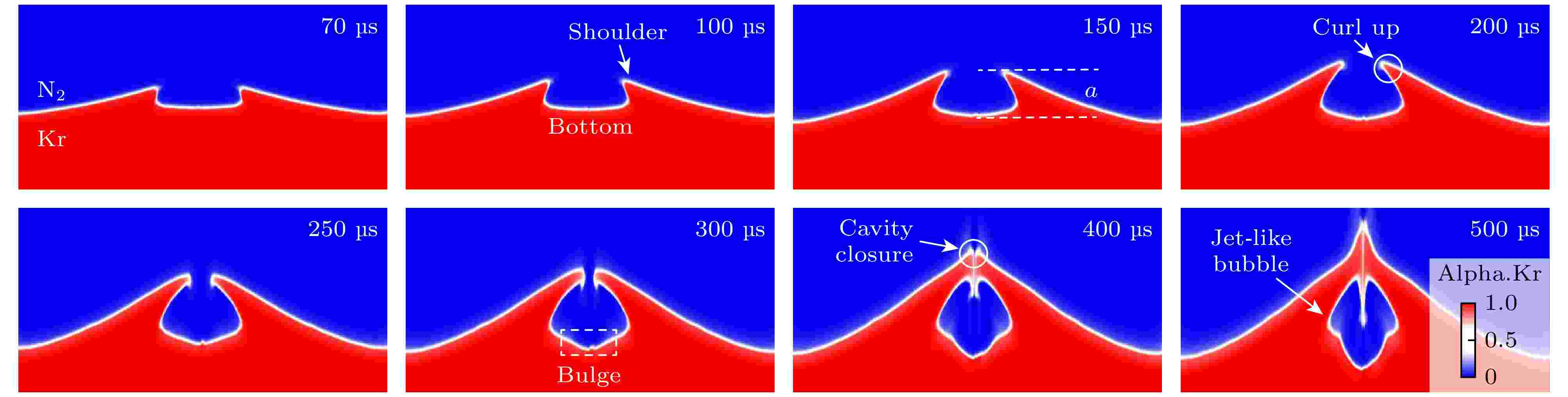
In order to better understand and predict the complex interface instability phenomena induced by non-uniform shock waves in practical engineering and scientific applications, a detailed investigation has been conducted on the interaction between a Mach reflection wave configuration and a planar gas interface. Particular attention is paid to the role of the Mach stem scale in governing the evolution of interface instability and the associated mechanisms of perturbation growth. Numerical simulations show that when the Mach reflection wave configuration interacts with the interface, the complex wave structures impart initial velocity perturbations onto the interface, thereby triggering instability. This process is further influenced by the non-uniform post-shock flow field, under which the initially perturbed interface gradually evolves into a concave cavity and subsequently into jet-like bubble structures. These patterns are notably different from the spike and bubble morphologies observed in classical Richtmyer-Meshkov instability. A systematic quantitative analysis of the perturbation amplitude reveals that the instability growth can be divided into two different stages: an initial linear growth stage and a nonlinear development stage. The transition between these stages is governed by interface deformation mechanisms, particularly the bending of the slip line intersecting the interface and the subsequent formation of the curl-up jet. When the shock strength and incidence angle of the Mach reflection configuration are kept constant, the Mach stem scale emerges as the decisive parameter controlling the characteristic time of slip line curling and jet development. The results show that during the linear stage, perturbation growth is primarily determined by shock strength and incidence angle, and is insensitive to the Mach stem scale. In contrast, during the nonlinear stage, the perturbation growth rate increases with the augmentation of Mach stem scales, highlighting the scale-dependent nature of the nonlinear stage. Furthermore, theoretical models are critically examined against numerical simulation results. While existing models can reasonably capture the initial velocity perturbations imprinted on the interface by the Mach reflection configuration, they are unable to combine the effects of Mach stem scale and the sustained driving influence of post-shock flow non-uniformities. This limitation underscores the need for improved theoretical descriptions. Overall, these findings provide new insights into the intrinsic coupling among shock strength, incidence angle, and Mach stem scale in determining the evolution of shock-induced interface instability. These insights not only deepen the fundamental understanding of the non-stand RM instability but also provide valuable references for the development of predictive theoretical models and the engineering applications such as inertial confinement fusion and high-speed propulsion systems.
EDITOR'S SUGGESTION
2025, 74 (24): 245202.
doi: 10.7498/aps.74.20251047
Abstract +
In radio-frequency capacitively coupled dusty plasma discharge, the grooves on the lower electrode plate significantly modify the electric potential distribution in the sheath region, thereby influencing the collective dynamic behavior of dust particles. Experimentally, when micrometer-sized dust particles are injected into the discharge chamber, a distinct layer of dust particles forms above the groove-induced potential well, exhibiting a characteristic bowl-shaped cloud structure. The volume of the dust cloud shows a strong dependence on RF power and discharge pressure. As power increases or pressure decreases, the dust cloud moves upward due to the influence of axial force on the particles. Besides, dust voids form in the middle of each dust layer, and their diameter evolution is influenced by particle number, RF power, and pressure. Particularly, when the diameters of the electrode grooves are small, the diameters of the dust voids first increase, then decrease and finally disappear as discharge pressure increases. Furthermore, a hybrid model is theoretically established. This model couples a fluid model with a dust particle model to explain the collective behavior of dust particles. This behavior is governed by the resultant axial force which includes axial electric field force, ion drag force, and gravity, as well as the resultant radial force, which considers radial electric field force and ion drag force. It is also found that in the DC-overlapped RF plasma, the suspension height of dust particles first increases and then decreases as the negative DC bias is increased. The change in dust particle height can reflect the transition of plasma discharge from α -mode to γ -mode.
CONDENSED MATTER: STRUCTURAL, MECHANICAL, AND THERMAL PROPERTIES
2025, 74 (24): 246202.
doi: 10.7498/aps.74.20251044
Abstract +
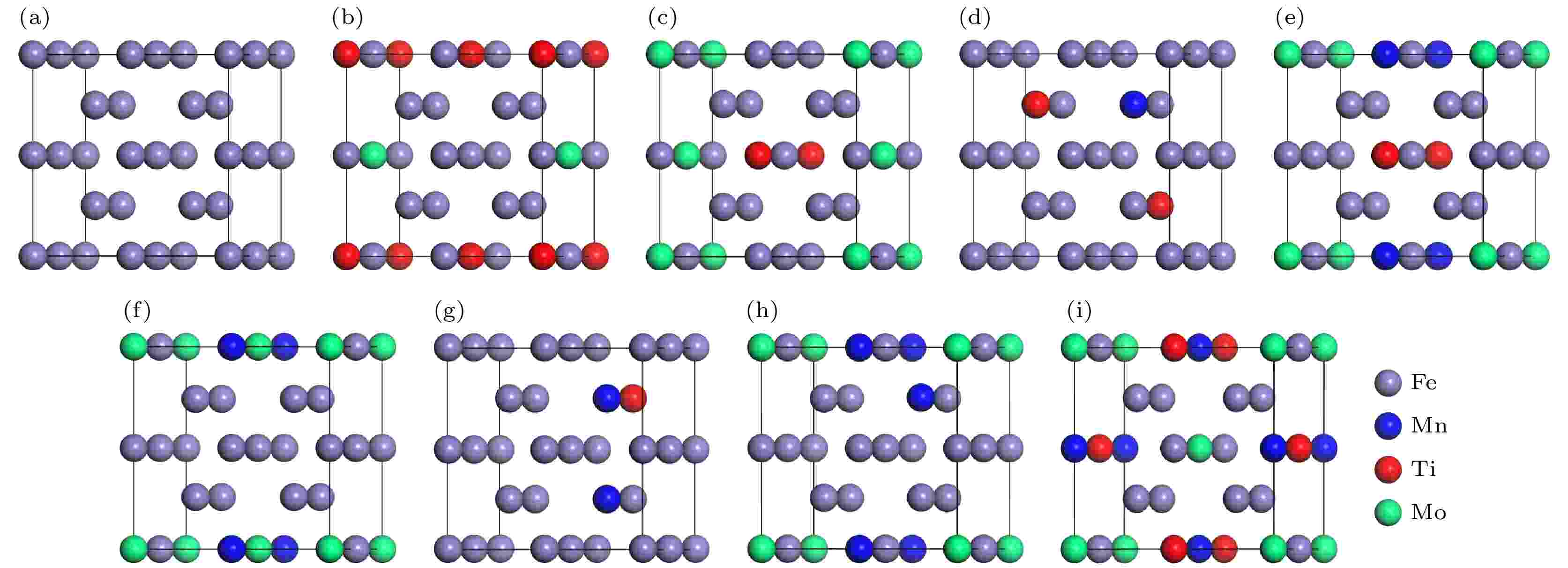
Ferrite (α-Fe), as a fundamental phase of steel materials, plays a decisive role in determining their macroscopic mechanical behaviors through its microscopic properties, particularly in engineering applications involving resistance to plastic deformation and fracture, fatigue resistance, wear resistance, and low-temperature toughness. Therefore, alloying elements are commonly introduced to improve the performance of steel via mechanisms such as grain refinement strengthening and precipitation strengthening. However, in these strengthening mechanisms, the effects of doped alloying elements on the stability, electronic structure, and mechanical properties of ferrite itself have not been thoroughly investigated. In this study, orthogonal experimental design and first-principles calculations are employed to investigate the effects of ternary alloy doping with M (Mn, Ti, Mo) on the stabilities, electronic structures, and mechanical properties of a ferrite-based supercell model Fe16 – x – y – zMnxTiyMoz (x, y, or z = 0, 1, or 2), aiming to provide both theoretical insight and experimental reference for improving the comprehensive performance of ferrite-based steels by modifying the properties of the matrix phase. The results of the formation enthalpy (Hform) calculations indicate that all solid solutions have negative formation enthalpies, suggesting that they can form spontaneously. Among them, Ti doping is the most favorable for solid solution formation, followed by Mn, with Mo being the least favorable. The Fe13Ti1Mo2 configuration is the easiest to form spontaneously. The cohesive energy (Ecoh) results demonstrate that all solid solutions exhibit structural stabilities. Fe13Ti1Mo2 has the largest (most negative) cohesive energy of –477.96 eV, indicating that it possesses the highest structural stability. The contribution of Mo doping to stability enhancement is the greatest, followed by Ti, while the influence of Mn is the smallest. Electronic structure calculations reveal that M doping consistently reduces the density of states (DOS) at the Fermi level for Fe16 – x – y – zMnxTiyMoz. The lowest DOS at the Fermi level is found to be 4.294 in Fe13Ti1Mo2, indicating enhanced hybridization and overlap between Mn 3d, Ti 3d, Mo 4d, and Fe 3d states. This strong hybridization leads to a decrease in the Fermi level and contributes to the high stability of the Fe13Ti1Mo2 phase. Mechanical property calculations indicate that M doping reduces the Young’s modulus (E) and Vickers hardness (HV) of the solid solutions. However, the K values (K = GH/BH) are all greater than 1.75, and Poisson’s ratios (ν) exceed 0.26, implying that while stiffness and hardness decrease, the ductility of the materials is improved. This study provides valuable guidance for designing ductile and tough ferrite-based steel materials.
CONDENSED MATTER: ELECTRONIC STRUCTURE, ELECTRICAL, MAGNETIC, AND OPTICAL PROPERTIES
2025, 74 (24): 247401.
doi: 10.7498/aps.74.20251391
Abstract +
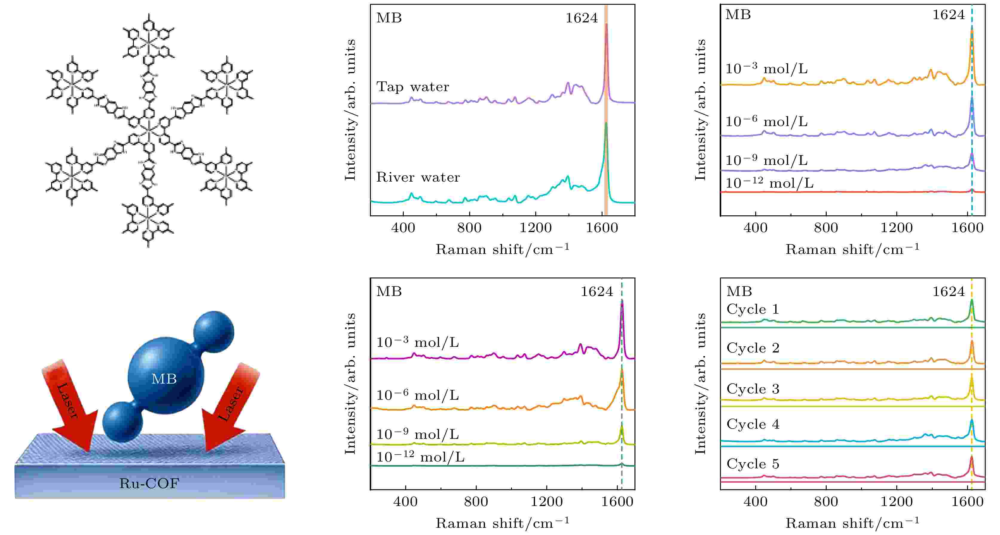
Covalent organic frameworks (COFs) have emerged as promising substrates for surface-enhanced Raman scattering (SERS) due to their highly ordered crystalline porous architecture, superior molecular adsorption and enrichment capabilities, and excellent thermal and chemical stability. However, pure COFs inherently lack plasmonic resonance and free electron density, resulting in limited electromagnetic enhancement and overall weak SERS signal, which hinders their practicality in ultrasensitive molecular detection applications. To overcome these limitations, this study aims to design and synthesize a novel ruthenium-based covalent organic framework composite (Ru-COF) by integrating ruthenium complexes directly into the COF skeleton, thereby creating a metal-organic, synergy-enhanced SERS substrate suited for trace analysis in real water. A Ru-COF is synthesized by solvothermal condensation of 1, 2, 4, 5-benzenetetramine (BTA·4HCl) with tris (4, 4'-dicarboxy-2, 2'-bipyridyl) ruthenium, forming Ru-N/O coordinated nodes within the framework. The material is characterizedusing X-ray diffraction (XRD) to confirm enhanced π-π stacking and new crystalline peaks at 10.2° and 16° in Ru-COF, Fourier-transform infrared spectroscopy (FT-IR) to verify amide and benzimidazole bond formations with shifts indicating Ru integration, Brunauer-Emmett-Teller (BET) analysis to reveal the increased specific surface areas (22.5 m2/g for Ru-COF vs. 17.2 m2/g for COF), and scanning electron microscopy (SEM) with energy-dispersive X-ray spectroscopy (EDS) mapping to show uniform distribution of C, N, O, and Ru elements in a dense layered morphology. SERS performance is evaluated using methylene blue (MB) as a probe molecule on a Renishaw InVia Raman spectrometer (514.5 nm excitation, 40 mW power, 10 s exposure), with additional tests on 4-mercaptobenzoic acid (4-MBA) for universality assessment. Enhancement mechanisms are analyzed through energy level alignments, with Ru-COF’s HOMO/LUMO at –0.95 eV/–1.12 eV (vs. vacuum) facilitating hole-injection charge transfer to MB’s levels (–2.34 eV/–4.15 eV), enhancing polarizability derivatives and Raman cross-sections via Herzberg-Teller coupling. The results demonstrate that Ru-COF exhibits superior SERS activity compared with pure COF and Ag-COF. For MB detection, the characteristic peak at 1624 cm–1 shows an analytical enhancement factor (EF) of 1.83 × 10¹⁰, calculated from normalized intensities and molecular densities, which far exceeds COF’s performance. Concentration-dependent spectra reveal a linear response from 10–3 to 10–13 mol/L (R2 = 0.997), with a limit of detection (LOD, S/N = 3) of 4.16 × 10⁻¹² mol/L. Signal reproducibility is excellent, with a relative standard deviation (RSD) of 3.41% across 10 random spots. Cycling tests (5 repetitions) retain 90.2% of initial intensity, and long-term stability assessment shows 85.7% signal retention after four-months of air exposure. For 4-MBA, non-resonant enhancement yields an LOD of 10–12 mol/L, dominated by CM via interfacial coordination and π-π interactions. In complex matrices such as tap and river water, Ru-COF maintains LODs of 5.2 × 10⁻¹² mol/L and 6.8 × 10⁻¹² mol/L, respectively, with 91% signal retention after five cycles, demonstrating robust anti-interference against ions (e.g., Cl–, ${\rm SO}^{2-}_4 $) and organic impurities, attributed to the hydrophobic porous structure and stable Ru coordination. In conclusion, the Ru-COF composite represents a breakthrough in SERS substrate design by achieving ultrasensitive detection through EM-CM synergy, with key physical outcomes including high EF, sub-picomolar LODs, and exceptional spatiotemporal stability. This work provides a novel paradigm for metal-embedded COFs in plasmonic sensing and lays the groundwork for practical applications in environmental monitoring, food safety, and biomedical diagnostics.
2025, 74 (24): 247901.
doi: 10.7498/aps.74.20251188
Abstract +
The virtual cathode is an important phenomenon in thermionic emission, and it is widely present in various electronic devices and systems such as vacuum tubes, electron guns, high-power microscopes, X-ray tubes, concentrated solar thermionic converters, and emissive probes. Since the virtual cathode can directly affect the performance of these devices, it is of great significance to study the characteristics of the virtual cathode and conduct experimental measurements on it. In our recent research, a one-dimensional model of thermionic emission was established, and the analytical expressions for the potential barrier and the spatial width of the virtual cathode were derived. With the development of virtual cathode theories, measuring the virtual cathode experimentally has become a reality. In this study, based on our one-dimensional theoretical model, the absolute error theory of the virtual cathode is established, and the contributions of different parameters, such as the hot-cathode temperature, the saturated electron emission current, the electron collection current, Dushman constant, and the work function of hot cathodes, to the absolute errors in the virtual cathode measurement are systematically analyzed. The research results show that the main factors affecting the measurement of the virtual cathode potential are closely related to the size of the virtual cathode. When the virtual cathode potential generated by hot-cathodes is strong, the uncertainty of the hot-cathode temperature becomes the main error source, with a probability of about 61% for the potential barrier measurement, but when the virtual cathode is weak, the main factor becomes the uncertainty of the electron current measurement with a probability of about 39%. Besides, when measuring the virtual cathode width, for common hot-cathodes such as oxide (BaO) cathode, tungsten cathode, and molybdenum cathode, the main factors affecting the measurement results are the uncertainties in the hot-cathode temperature and the work function. These uncertainties account for approximately 94%, 96% and 97% of the measurement variability, corresponding to the above three cathodes, respectively. Only when the virtual cathode is very weak, does the uncertainty of the electron current become the main error source for the measurement of the virtual cathode width.
INTERDISCIPLINARY PHYSICS AND RELATED AREAS OF SCIENCE AND TECHNOLOGY
2025, 74 (24): 248501.
doi: 10.7498/aps.74.20251004
Abstract +
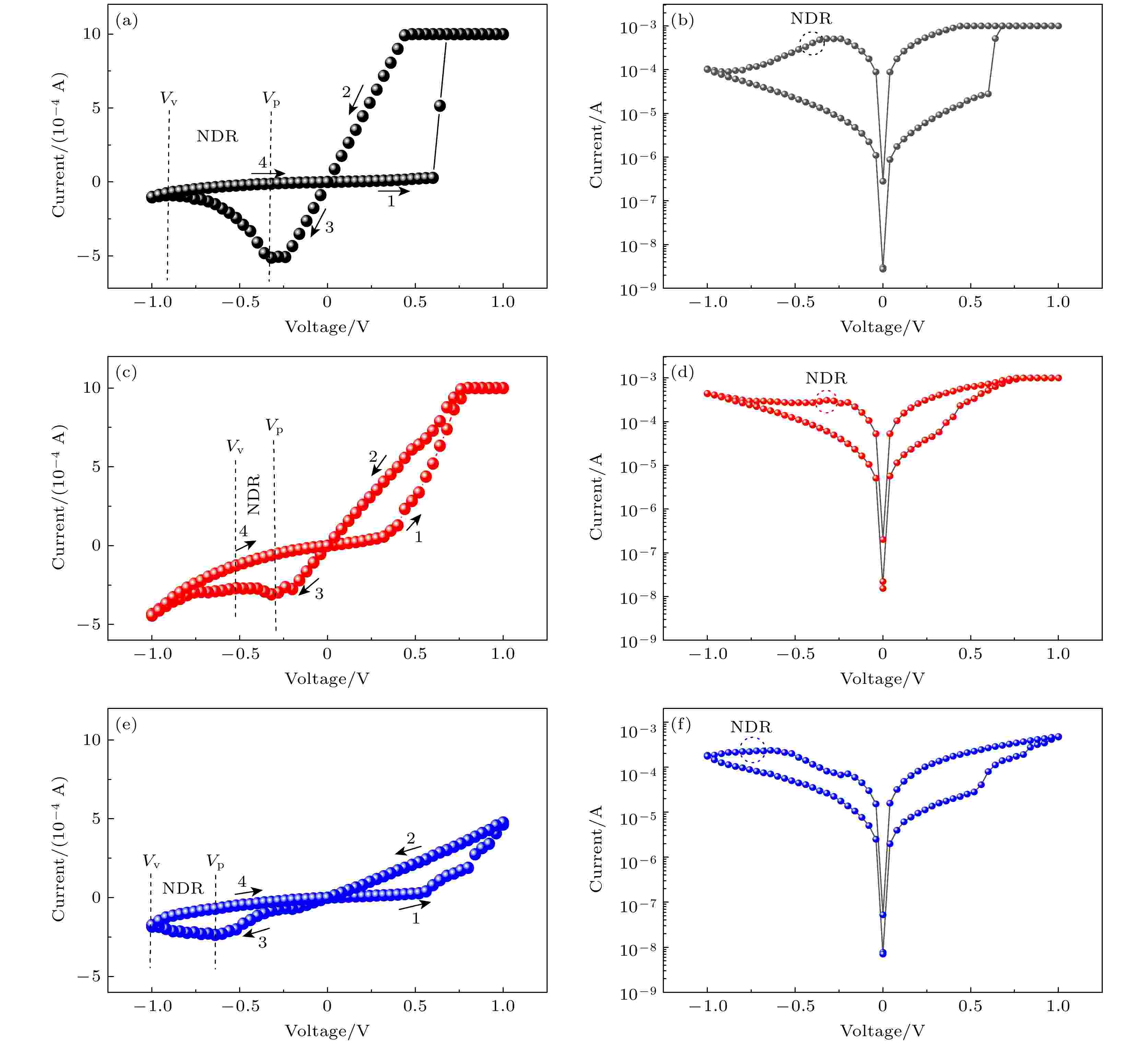
In this paper, the resistive switching characteristics of Ag/BiFeO3/Fe2O3/ITO multilayer film deposited on ITO by magnetron sputtering are investigated. The Ag/BiFeO3/Fe2O3/ITO devices all exhibit superior resistive switching behaviors due to the formation of Ag conducting filaments. The resistive switching ratio of the device is close to 10 for the sample with 100 nm-thick Fe2O3 film. The current value of the device increases sharply at 0.56 V when the voltage is swept forward, and the device switches from LRS back to HRS at –0.3 V when a voltage of opposite polarity is applied. The I-V curves of the device are fitted in double logarithmic coordinates. It is found that the device is controlled by an Ohmic conduction model in the low resistance state and by two conduction models in the high resistance state: Ohmic conduction in the low bias region, and the SCLC conduction model at higher voltages. Such a resistive switching characteristic with very low switching voltage and a high resistance ratio is particularly important for the application of resistive stochastic storage. In addition, all samples show an obvious negative differential resistance effect, which is caused by Joule heating. The Ag/BiFeO3/Fe2O3/ITO device show both resistive switching characteristics and a negative differential resistance effect, which have important applications.
2025, 74 (24): 248502.
doi: 10.7498/aps.74.20250891
Abstract +
