


-
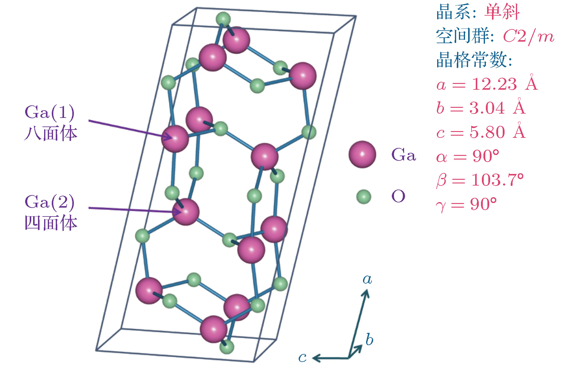
Gallium oxide (Ga2O3), with a bandgap of about 4.9 eV, is a new type of ultra-wide bandgap semiconductor material. The Ga2O3 can crystallize into five different phases, i.e. α, β, γ, δ, and ε-phase. Among them, the monoclinic β-Ga2O3 (space group: C2/m) with the lattice parameters of a = 12.23 Å, b = 3.04 Å, c = 5.80 Å, and β = 103.7° has been recognized as the most stable phase. The β-Ga2O3 can be grown in bulk form from edge-defined film-fed growth with a low-cost method. With a high theoretical breakdown electrical field (8 MV/cm) and large Baliga’s figure of merit, the β-Ga2O3 is a potential candidate material for next-generation high-power electronics (including diode and field effect transistor) and extreme environment electronics [high temperature, high radiation, and high voltage (low power) switching]. Due to a high transmittance to the deep ultraviolet-visible light with a wavelength longer than 253 nm, the β-Ga2O3 is a natural material for solar-blind ultraviolet detection and deep-ultraviolet transparent conductive electrode. In this paper, the crystal structure, physical properties and device applications of Ga2O3 material are introduced. And the latest research progress of β-Ga2O3 in deep ultraviolet transparent conductive electrode and solar-blind ultraviolet photodetector are reviewed. Although Sn doped Ga2O3 thin film has a conductivity of up to 32.3 S/cm and a transmittance greater than 88%, there is still a long way to go for commercial transparent conductive electrode. At the same time, the development history of β-Ga2O3 solar-blind ultraviolet photodetectors based on material type (nanometer, single crystal and thin film) is described in chronological order. The photodetector based on quasi-two-dimensional β-Ga2O3 flakes shows the highest responsivity (1.8 × 10⁵ A/W). The photodetector based on ZnO/Ga2O3 core/shell micron-wire has a best comprehensive performance, which exhibits a responsivity of 1.3 × 10³ A/W and a response time ranging from 20
${\text{μ}}{\rm{s}}$ to 254 nm light at –6 V. We look forward to applying the β-Ga2O3 based solar-blind ultraviolet photodetectors to military (such as: missile early warning and tracking, ultraviolet communication, harbor fog navigation, and so on) and civilian fields (such as ozone hole monitoring, disinfection and sterilization ultraviolet intensity monitoring, high voltage corona detection, forest fire ultraviolet monitoring, and so on).-
Keywords:
- gallium oxide /
- ultra-wide bandgap semiconductor /
- solar-blind photodetector /
- ultraviolet transparent electrode
[1] 程轶 2013 博士学位论文(大连: 大连理工大学)
Cheng Y 2013 Ph. D. Dissertation (Dalian: Dalian University of Technology) (in Chinese)
[2] 马海林, 苏庆 2014 物理学报 63 116701
 Google Scholar
Ma H L, Su Q 2014 Acta Phys. Sin. 63 116701
Google Scholar
[3] 潘惠平, 成枫锋, 李琳, 洪瑞华, 姚淑德 2013 物理学报 62 048801
Google Scholar
Pan H P, Cheng F F, Li L, Hong R H, Yao S D 2013 Acta Phys. Sin. 62 048801
Google Scholar
[4] Roy R, Hill V G, Osborn E F 1952 J. Am. Chem. Soc. 74 719
Google Scholar
[5] Kaneko K, Nomura T, Kakeya I, Fujita S 2009 Appl. Phys. Express 2 075501
Google Scholar
[6] Fujita S, Kaneko K 2014 J. Cryst. Growth 401 588
Google Scholar
[7] Shinohara D, Fujita S 2008 Jpn. J. Appl. Phys. 47 7311
Google Scholar
[8] Schewski R, Wagner G, Baldini M, Gogova D, Galazka Z, Schulz T, Remmele T, Markurt T, Wenckstern H V, Grundmann M, Bierwagen O, Vogt P, Albrecht M 2015 Appl. Phys. Express 8 011101
Google Scholar
[9] Lee S D, Akaiwa K, Fujita S 2013 Phys. Status Solidi C 10 1592
Google Scholar
[10] Lee S D, Ito Y, Kaneko K, Fujita S 2015 Jpn. J. Appl. Phys. 54 030301
Google Scholar
[11] Kaneko K, Nomura T, Fujita S 2010 Phys. Status Solidi C 7 2467
Google Scholar
[12] Kaneko K, Kakeya I, Komori S, Fujita S 2013 J. Appl. Phys. 113 233901
Google Scholar
[13] Mitome M, Kohiki S, Nagai T, Kurashima K, Kimoto K, Bando Y 2013 Cryst. Growth Des. 13 3577
Google Scholar
[14] Wang T, Farvid S S, Abulikemu M, Radovanovic P V 2010 J. Am. Chem. Soc. 132 9250
Google Scholar
[15] Playford H Y, Hannon A C, Tucker M G, Dawson D M, Ashbrook S E, Kastiban R J, Sloan J, Walton R I 2014 J. Phys. Chem. C 118 16188
Google Scholar
[16] Lorenzi R, Paleari A, Golubev N V, Ignat'eva E S, Sigaev V N, Niederberger M, Lauria A 2015 J. Mater. Chem. C 3 41
Google Scholar
[17] Takahashi M, Nakatani T, Iwamoto S, Watanabe T, Inoue M 2006 J. Phys. Condens Matter 18 5745
Google Scholar
[18] Oshima Y, Víllora E G, Matsushita Y, Yamamoto S, Shimamura K 2015 J. Appl. Phys. 118 085301
Google Scholar
[19] Ge S X, Zheng Z 2009 Solid State Sci. 11 1592
Google Scholar
[20] Tsuchiya T, Yusa H, Tsuchiya J 2007 Phys. Rev. B 76 174108
Google Scholar
[21] Bermudez V M 2006 Chem. Phys. 323 193
Google Scholar
[22] Yamaga M, Víllora E G, Shimamura K, Ichinose N, Honda M 2003 Phys. Rev. B 68 155207
Google Scholar
[23] Zacherle T, Schmidt P C, Martin M 2013 Phys. Rev. B 87 235206
Google Scholar
[24] Orita M, Hiramatsu H, Ohta H, Hirano M, Hosono H 2002 Thin Solid Films 411 134
Google Scholar
[25] Higashiwaki M, Sasaki K, Kuramata A, Masui T, Yamakoshi S 2012 Appl. Phys. Lett. 100 013504
Google Scholar
[26] Dong L, Jia R, Xin B, Zhang Y 2016 J. Vac. Sci. Technol., A 34 060602
[27] Dong L, Jia R, Xin B, Peng B, Zhang Y 2017 Sci. Rep. 7 40160
Google Scholar
[28] Tao X T 2019 J. Semicond. 40 010401
Google Scholar
[29] Fu B, Jia Z T, Mu W X, Yin Y R, Zhang J, Tao X T 2019 J. Semicond. 40 011804
Google Scholar
[30] Mohamed H F, Xia C T, Sai Q L, Cui H Y, Pan M Y, Qi H J 2019 J. Semicond. 40 011801
Google Scholar
[31] Higashiwaki M, Sasaki K, Murakami H, Kumagai Y, Koukitu A, Kuramata A, Masui T, Yamakoshi S 2016 Semicond. Sci. Technol. 31 034001
Google Scholar
[32] Razeghi M 2002 Proc. IEEE 90 1006
Google Scholar
[33] Du X, Mei Z, Liu Z, Guo Y, Zhang T, Hou Y, Zhang Z, Xue Q, Kuznetsov A Y 2009 Adv. Mater. 21 4625
Google Scholar
[34] Higashiwaki M, Sasaki K, Kuramata A, Masui T, Yamakoshi S 2014 Phys. Status Solidi A 211 21
Google Scholar
[35] Higashiwaki M, Jessen G H 2018 Appl. Phys. Lett. 112 060401
Google Scholar
[36] Villora E G, Arjoca S, Shimamura K, Inomata D, Aoki K 2014 Proc. of SPIE 8987 1
[37] Wellenius P, Suresh A, Foreman J V, Everitt H O, Muth J F 2008 Mater. Sci. Eng. B 146 252
Google Scholar
[38] Wellenius P, Suresh A, Muth J F 2008 Appl. Phys. Lett. 92 021111
Google Scholar
[39] Vanithakumari S C, Nanda K K 2009 Adv. Mater. 21 3581
Google Scholar
[40] Lin C F, Chen K T, Huang K P 2010 IEEE Electron Device Lett. 31 1431
Google Scholar
[41] Choi S E, Oh Y T, Ham H K, Kim T W, Heo G S, Park J W, Choi B H, Shin D C 2011 Curr. Appl. Phys. 11 S255
[42] Iizuka K, Morishima Y, Kuramata A, Shen Y J, Tsai C Y, Su Y Y, Liu G, Hsu T C, Yeh J H 2015 Proc. of SPIE 9363 1
[43] Schwebel T, Fleischer M, Meixner H, Kohl C D 1998 Sens. Actuators B 49 46
Google Scholar
[44] Kohl D, Ochs T, Geyer W, Fleischer M, Meixner H 1999 Sens. Actuators B 59 140
Google Scholar
[45] Ogita M, Saika N, Nakanishi Y, Hatanaka Y 1999 Appl. Surf. Sci. 142 188
Google Scholar
[46] Schwebel T, Fleischer M, Meixner H 2000 Sens. Actuators B 65 176
Google Scholar
[47] Baban C, Toyoda Y, Ogita M 2005 Thin Solid Films 484 369
Google Scholar
[48] Bartic M, Toyoda Y, Baban C I, Ogita M 2006 Jpn. J. Appl. Phys., Part1 45 5186
Google Scholar
[49] Feng P, Xue X Y, Liu Y G, Wan Q, Wang T H 2006 Appl. Phys. Lett. 89 112114
Google Scholar
[50] Bartic M, Baban C I, Suzuki H, Ogita M, Isai M 2007 J. Am. Ceram. Soc. 90 2879
Google Scholar
[51] Liu Z F, Yamazaki T, Shen Y, Kikuta T, Nakatani N, Li Y 2008 Sens. Actuators B 129 666
Google Scholar
[52] Arnold S P, Prokes S M, Perkins F K, Zaghloul M E 2009 Appl. Phys. Lett. 95 103102
Google Scholar
[53] Lee C T, Yan J T 2010 Sens. Actuators B 147 723
Google Scholar
[54] Hou Y, Jayatissa A H 2014 Sens. Actuators B 204 310
Google Scholar
[55] Bartic M 2015 Phys. Status Solidi A 211 40
[56] Hayashi H, Huang R, Ikeno H, Oba F, Yoshioka S, Tanaka I, Sonoda S 2006 Appl. Phys. Lett. 89 181903
Google Scholar
[57] Pei G, Xia C, Dong Y, Wu B, Wang T, Xu J 2008 Scr. Mater. 58 943
Google Scholar
[58] Guo D Y, Wu Z P, An Y H, Li X J, Guo X C, Chu X L, Sun C L, Lei M, Li L H, Cao L X, Li P G, Tang W H 2015 J. Mater. Chem. C 3 1830
Google Scholar
[59] Guo D Y, Wu Z P, Li P G, Wang Q J, Lei M, Li L H, Tang W H 2015 RSC Adv. 5 12894
Google Scholar
[60] Guo D Y, An Y H, Cui W, Zhi Y S, Zhao X L, Lei M, Li L H, Li P G, Wu Z P, Tang W H 2016 Sci. Rep. 6 25166
Google Scholar
[61] Gao X, Xia Y, Ji J, Xu H, Su Y, Li H, Yang C, Guo H, Yin J, Liu Z 2010 Appl. Phys. Lett. 97 193501
Google Scholar
[62] Yang J B, Chang T C, Huang J J, Chen S C, Yang P C, Chen Y T, Tseng H C, Sze S M, Chu A K, Tsai M J 2013 Thin Solid Films 529 200
Google Scholar
[63] Aoki Y, Wiemann C, Feyer V, Kim H S, Schneider C M, Ill-Yoo H, Martin M 2014 Nat. Commun. 5 3473
Google Scholar
[64] Hsu C W, Chou L J 2012 Nano Lett. 12 4247
Google Scholar
[65] Lee D Y, Tseng T Y 2011 J. Appl. Phys. 110 114117
Google Scholar
[66] Huang J J, Chang T C, Yang J B, Chen S C, Yang P C, Chen Y T, Tseng H C, Sze S M, Chu A K, Tsai M J 2012 IEEE Electron Device Lett. 33 1387
Google Scholar
[67] Yang J B, Chang T C, Huang J J, Chen Y T, Yang P C, Tseng H C, Chu A K, Sze S M, Tsai M J 2013 Thin Solid Films 528 26
Google Scholar
[68] Guo D Y, Wu Z P, An Y H, Li P G, Wang P C, Chu X L, Guo X C, Zhi Y S, Lei M, Li L H, Tang W H 2015 Appl. Phys. Lett. 106 042105
Google Scholar
[69] Guo D Y, Wu Z P, Zhang L J, Yang T, Hu Q R, Lei M, Li P G, Li L H, Tang W H 2015 Appl. Phys. Lett. 107 032104
Google Scholar
[70] Guo D Y, Qian Y P, Su Y L, Shi H Z, Li P G, Wu J T, Wang S L, Cui C, Tang W H 2017 AIP Adv. 7 065312
Google Scholar
[71] Wang P C, Li P G, Zhi Y S, Guo D Y, Pan A Q, Zhan J M, Liu H, Shen J Q, Tang W H 2015 Appl. Phys. Lett. 107 262110
Google Scholar
[72] Gollakota P, Dhawan A, Wellenius P, Lunardi L M, Muth J F, Saripalli Y N 2006 Appl. Phys. Lett. 88 221906
Google Scholar
[73] Sawada K, Adachi S 2014 ECS J. Solid State Sci. 3 R238
Google Scholar
[74] Kang B K, Mang S R, Lim H D, Song K M, Song Y H, Go D H, Jung M K, Senthil K, Yoon D H 2014 Mater. Chem. Phys. 147 178
Google Scholar
[75] Wu Z, Bai G, Hu Q, Guo D, Sun C, Ji L, Lei M, Li L, Li P, Hao J, Tang W 2015 Appl. Phys. Lett. 106 171910
Google Scholar
[76] Wu Z, Bai G, Qu Y, Guo D, Li L, Li P, Hao J, Tang W 2016 Appl. Phys. Lett. 108 211903
Google Scholar
[77] Li W, Peng Y, Wang C, Zhao X, Zhi Y, Yan H, Li L, Li P, Yang H, Wu Z, Tang W 2017 J. Alloys Compd. 697 388
Google Scholar
[78] Orita M, Ohta H, Hirano M, Hosono H 2000 Appl. Phys. Lett. 77 4166
Google Scholar
[79] Suzuki N, Ohira S, Tanaka M, Sugawara T, Nakajima K, Shishido T 2007 Phys. Status Solidi C 4 2310
Google Scholar
[80] Ou S L, Wuu D S, Fu Y C, Liu S P, Horng R H, Liu L, Feng Z C 2012 Mater. Chem. Phys. 133 700
Google Scholar
[81] Du X J, Li Z, Luan C N, Wang W G, Wang M X, Feng X J, Xiao H D, Ma J 2015 J. Mater. Sci. 50 3252
Google Scholar
[82] Mi W, Li Z, Luan C N, Xiao H D, Zhao C S, Ma J 2015 Ceram. Int. 41 2572
Google Scholar
[83] Minami T, Takeda Y, Kakumu T, Takata S, Fukuda I 1997 J. Vac. Sci. Technol., A 15 958
Google Scholar
[84] Kim S, Kim S J, Kim K H, Kim H D, Kim T G 2014 Phys. Status Solidi A 211 2569
Google Scholar
[85] Kim S J, Park S Y, Kim K H, Kim S W, Kim T G 2014 IEEE Electron Device Lett. 35 232
Google Scholar
[86] Woo K Y, Lee J H, Kim K H, Kim S J, Kim T G 2014 Phys. Status Solidi A 211 1760
Google Scholar
[87] Zhuang H H, Yan J L, Xu C Y, Meng D L 2014 Appl. Surf. Sci. 307 241
Google Scholar
[88] Li Y, Tokizono T, Liao M, Zhong M, Koide Y, Yamada I, Delaunay J J 2010 Adv. Funct. Mater. 20 3972
Google Scholar
[89] Oshima T, Okuno T, Arai N, Suzuki N, Hino H, Fujita S 2009 Jpn. J. Appl. Phys. 48 011605
Google Scholar
[90] Oshima T, Okuno T, Fujita S 2007 Jpn. J. Appl. Phys. 46 7217
Google Scholar
[91] Feng P, Zhang J Y, Li Q H, Wang T H 2006 Appl. Phys. Lett. 88 153107
Google Scholar
[92] Weng W Y, Hsueh T J, Chang S J, Huang G J, Chang S P 2010 IEEE Photonics Technol. Lett. 22 709
Google Scholar
[93] Wu Y L, Chang S J, Weng W Y, Liu C H, Tsai T Y, Hsu C L, Chen K C 2013 IEEE Sens. J. 13 2368
Google Scholar
[94] Li L, Auer E, Liao M, Fang X, Zhai T, Gautam U K, Lugstein A, Koide Y, Bando Y, Golberg D 2011 Nanoscale 3 1120
Google Scholar
[95] Tian W, Zhi C, Zhai T, Chen S M, Wang X, Liao M Y, Golberg D, Bando Y 2012 J. Mater. Chem. 22 17984
Google Scholar
[96] Feng W, Wang X N, Zhang J, Wang L, Zheng W, Hu P, Cao W, Yang B 2014 J. Mater. Chem. C 2 3254
Google Scholar
[97] Teng Y, Song L X, Ponchel A, Yang Z K, Xia J 2014 Adv. Mater. 26 6238
Google Scholar
[98] Zou R J, Zhang Z Y, Liu Q, Hu J Q, Sang L W, Liao M Y, Zhang W J 2014 Small 10 1848
Google Scholar
[99] Zhong M Z, Wei Z M, Meng X Q, Wu F, Li J 2015 J. Alloys Compd. 619 572
Google Scholar
[100] Zhao B, Wang F, Chen H Y, Wang Y P, Jiang M M, Fang X S, Zhao D X 2015 Nano Lett. 15 3988
Google Scholar
[101] Zhao B, Wang F, Chen H, Zheng L, Su L, Zhao D, Fang X 2017 Adv. Funct. Mater. 27 1700264
Google Scholar
[102] Chen X, Liu K, Zhang Z, Wang C, Li B, Zhao H, Zhao D, Shen D 2016 ACS Appl. Mater. Interfaces 8 4185
Google Scholar
[103] Oh S, Kim J, Ren F, Pearton S J, Kim J 2016 J. Mater. Chem. C 4 9245
Google Scholar
[104] Kwon Y, Lee G, Oh S, Kim J, Pearton S J, Ren F 2017 Appl. Phys. Lett. 110 131901
Google Scholar
[105] Oh S, Mastro M A, Tadjer M J, Kim J 2017 ECS J. Solid State. Sci. 6 Q79
Google Scholar
[106] Oh S, Kim C K, Kim J 2017 ACS Photonics 5 1123
[107] Du J, Xing J, Ge C, Liu H, Liu P, Hao H, Dong J, Zheng Z, Gao H 2016 J. Phys. D: Appl. Phys. 49 425105
Google Scholar
[108] He T, Zhao Y, Zhang X, Lin W, Fu K, Sun C, Shi F, Ding X, Yu G, Zhang K, Lu S, Zhang X, Zhang B 2018 Nanophotonics 7 1557
Google Scholar
[109] Oshima T, Okuno T, Arai N, Suzuki N, Ohira S, Fujita S 2008 Appl. Phys. Express 1 011202
Google Scholar
[110] Suzuki R, Nakagomi S, Kokubun Y, Arai N, Ohira S 2009 Appl. Phys. Lett. 94 222102
Google Scholar
[111] Suzuki R, Nakagomi S, Kokubun Y 2011 Appl. Phys. Lett. 98 131114
Google Scholar
[112] Kong W Y, Wu G A, Wang K Y, Zhang T F, Zou Y F, Wang D D, Luo L B 2016 Adv. Mater. 28 10725
Google Scholar
[113] Mu W, Jia Z, Yin Y, Hu Q, Zhang J, Feng Q, Hao Y, Tao X 2017 CrystEngComm 19 5122
Google Scholar
[114] Yang C, Liang H, Zhang Z, Xia X, Tao P, Chen Y, Zhang H, Shen R, Luo Y, Du G 2018 RSC Adv. 8 6341
Google Scholar
[115] Ji Z, Du J, Fan J, Wang W 2006 Opt. Mater. 28 415
Google Scholar
[116] Kokubun Y, Miura K, Endo F, Nakagomi S 2007 Appl. Phys. Lett. 90 031912
Google Scholar
[117] Weng W Y, Hsueh T J, Chang S J, Huang G J, Hsueh H T 2011 IEEE Sens. J. 11 999
Google Scholar
[118] Huang Z D, Weng W Y, Chang S J, Chiu C, Wu S, Hsueh T 2013 IEEE Sens. J. 13 3462
Google Scholar
[119] Huang Z D, Weng W Y, Chang S J, Hua Y F, Chiu C J, Hsueh T J, Wu S L 2013 IEEE Sens. J. 13 1187
Google Scholar
[120] Huang Z D, Weng W Y, Chang S J, Hua Y F, Chiu C J, Tsai T Y 2013 IEEE Photonics Technol. Lett. 25 809
[121] Nakagomi S, Momo T, Takahashi S, Kokubun Y 2013 Appl. Phys. Lett. 103 072105
Google Scholar
[122] Ravadgar P, Horng R H, Yao S D, Lee H Y, Wu R, Ou S L, Tu L W 2013 Opt. Express 21 24599
Google Scholar
[123] Guo D Y, Wu Z P, Li P G, An Y H, Liu H, Guo X C, Yan H, Wang G F, Sun C L, Li L H, Tang W H 2014 Opt. Mater. Express 4 1067
Google Scholar
[124] Wang X, Chen Z W, Guo D Y, Zhang X, Wu Z P, Li P G, Tang W H 2018 Opt. Mater. Express 8 2918
Google Scholar
[125] Peng Y K, Zhang Y, Chen Z W, Guo D Y, Zhang X, Li P G, Wu Z P, Tang W H 2018 IEEE Photonics Technol. Lett. 30 993
Google Scholar
[126] Guo D Y, Wu Z P, An Y H, Guo X C, Chu X L, Sun C L, Li L H, Li P G, Tang W H 2014 Appl. Phys. Lett. 105 023507
Google Scholar
[127] Guo D Y, Li P G, Wu Z P, Cui W, Zhao X L, Lei M, Li L H, Tang W H 2016 Sci. Rep. 6 24190
Google Scholar
[128] Qian Y P, Guo D Y, Chu X L, Shi H Z, Zhu W K, Wang K, Wang S L, Li P G, Zhang X H, Tang W H 2017 Mater. Lett. 209 558
Google Scholar
[129] Guo D Y, Qin X Y, Lv M, Shi H Z, Su Y L, Yao G S, Wang S L, Li C R, Li P G, Tang W H 2017 Electron. Mater. Lett. 13 483
Google Scholar
[130] Zhao X L, Cui W, Wu Z P, Guo D Y, Li P G, An Y H, Li L H, Tang W H 2017 J. Electron. Mater. 46 2366
Google Scholar
[131] Zhao X L, Wu Z P, Cui W, Zhi Y S, Guo D Y, Li L H, Tang W H 2017 ACS Appl. Mater. Interfaces 9 983
Google Scholar
[132] Zhao X L, Wu Z P, Guo D Y, Cui W, Li P G, An Y H, Li L H, Tang W H 2016 Semicond. Sci. Technol. 31 065010
Google Scholar
[133] Zhao X L, Zhi Y S, Cui W, Guo D Y, Wu Z P, Li P G, Li L H, Tang W H 2016 Opt. Mater. 62 651
Google Scholar
[134] Zhao X L, Wu Z P, Zhi Y S, An Y H, Cui W, Li L H, Tang W H 2017 J. Phys. D: Appl. Phys. 50 085102
Google Scholar
[135] Zhang M, Liu G H, Gu X H, Zhou J R 2014 Journal of Nanoscience and Nanotechnology 14 3827
Google Scholar
[136] Li W H, Zhao X L, Zhi Y S, Zhang X H, Chen Z W, Chu X L, Yang H J, Wu Z P, Tang W H 2018 Appl. Opt. 57 538
Google Scholar
[137] Guo D Y, Zhao X L, Zhi Y S, Cui W, Huang Y Q, An Y H, Li P G, Wu Z P, Tang W H 2016 Mater. Lett. 164 364
Google Scholar
[138] Ai M L, Guo D Y, Qu Y Y, Cui W, Wu Z P, Li P G, Li L H, Tang W H 2017 J. Alloys Compd. 692 634
Google Scholar
[139] An H Y, Chu X L, Huang Y Q, Zhi Y S, Guo D Y, Li P G, Wu Z P, Tang W H 2016 Prog. Nat. Sci. 26 65
Google Scholar
[140] Cui W, Guo D Y, Zhao X L, Wu Z P, Li P G, Li L H, Cui C, Tang W H 2016 RSC Adv. 6 100683
Google Scholar
[141] Huang Y Q, An Y H, Wu Z P, Guo D Y, Zhi Y S, Cui W, Zhao X L, Tang W H 2017 J. Alloys Compd. 717 8
Google Scholar
[142] Guo D Y, Liu H, Li P G, Wu Z P, Wang S L, Cui C, Li C R, Tang W H 2017 ACS Appl. Mater. Interfaces 9 1619
Google Scholar
[143] Guo X C, Hao N H, Guo D Y, Wu Z P, An Y H, Chu X L, Li L H, Li P G, Lei M, Tang W H 2016 J. Alloys Compd. 660 136
Google Scholar
[144] Guo D Y, Shi H Z, Qian Y P, Lv M, Li P G, Su Y L, Liu Q, Chen K, Wang S L, Cui C, Li C R, Tang W H 2017 Semicond. Sci. Technol. 32 03LT1
[145] Wu Z P, Jiao L, Wang X L, Guo D Y, Li W H, Li L H, Huang F, Tang W H 2017 J. Mater. Chem. C 5 8688
Google Scholar
[146] Li P G, Shi H Z, Chen K, Guo D Y, Cui W, Zhi Y S, Wang S L, Wu Z P, Chen Z W, Tang W H 2017 J. Mater. Chem. C 5 10562
Google Scholar
[147] Guo D Y, Su Y L, Shi H Z, Li P G, Zhao N, Ye J H, Wang S L, Liu A P, Chen Z W, Li C R, Tang W H 2018 ACS Nano 12 12827
Google Scholar
[148] An H Y, Zhi Y S, Wu Z P, Cui W, Zhao X L, Guo D Y, Li P G, Tang W H 2016 Appl. Phys. A 122 1036
Google Scholar
[149] Qu Y Y, Wu Z P, Ai M L, Guo D Y, An Y H, Yang H J, Li L H, Tang W H 2016 J. Alloys Compd. 680 247
Google Scholar
[150] An Y H, Guo D Y, Li S Y, Wu Z P, Huang Y Q, Li P G, Li L H, Tang W H 2016 J. Phys. D: Appl. Phys. 49 285111
Google Scholar
[151] Cui W, Zhao X L, An Y H, Guo D Y, Qing X Y, Wu Z P, Li P G, Li L H, Cui C, Tang W H 2017 J. Phys. D: Appl. Phys. 50 135109
Google Scholar
[152] Guo P, Xiong J, Zhao X H, Sheng T, Yue C, Tao B W, Liu X Z 2014 J. Mater. Sci. 25 3629
[153] Hu G C, Shan C X, Zhang N, Jiang M M, Wang S P, Shen D Z 2015 Opt. Express 23 13554
Google Scholar
[154] Sheng T, Liu X Z, Qian L X, Xu B, Zhang Y Y 2015 Rare Met.
Google Scholar
[155] Yu F P, Ou S L, Wuu D S 2015 Opt. Mater. Express 5 1240
Google Scholar
[156] Liu X Z, Guo P, Sheng T, Qian L X, Zhang W L, Li Y R 2016 Opt. Mater. 51 203
Google Scholar
[157] Qian L X, Liu X Z, Sheng T, Zhang W L, Li Y R, Lai P T 2016 AIP Adv. 6 045009
Google Scholar
[158] Liu X Z, Yue C, Xia C T, Zhang W L 2016 Chin. Phys. B 25 017201
Google Scholar
[159] Qian L X, Wu Z H, Zhang Y Y, Lai P T, Liu X Z, Li Y R 2017 ACS Photonics 4 2203
Google Scholar
[160] Feng Q, Huang L, Han G, Li F, Li X, Fang L, Xing X, Zhang J, Mu W, Jia Z, Guo D, Tang W, Tao X, Hao Y 2016 IEEE Trans. Electron Devices 63 3578
Google Scholar
[161] Feng Z Q, Huang L, Feng Q, Li X, Zhang H, Tang W H, Zhang J C, Hao Y 2018 Opt. Mater. Express 8 2229
Google Scholar
[162] Huang L, Feng Q, Han G Q, Li F G, Li X, Fang L W, Xing X Y, Zhang J C, Hao Y 2017 IEEE Photonics J. 9 6803708
[163] Zhang K, Feng Q, Huang L, Hu Z Z, Feng Z Q, Li A, Zhou H, Lu X L, Zhang C F, Zhang J C, Hao Y 2018 IEEE Photonics J. 10 6802508
[164] Feng Q, Li X, Han G, Huang L, Li F, Tang W, Zhang J, Hao Y 2017 Opt. Mater. Express 7 1240
Google Scholar
[165] Xu Y, An Z Y, Zhang L X, Feng Q, Zhang J C, Zhang C F, Hao Y 2018 Opt. Mater. Express 8 2941
Google Scholar
[166] Ahn S, Lin Y H, Ren F, Oh S, Jung Y, Yang G, Kim J, Mastro M A, Hite J K, Eddy C R, Pearton S J 2016 J. Vac. Sci. Technol. B 34 041213
Google Scholar
[167] Ahn S, Ren F, Oh S, Jung Y, Kim J, Mastro M A, Hite J K, Eddy C R, Pearton S J 2016 J. Vac. Sci. Technol. B 34 041207
Google Scholar
[168] Alema F, Hertog B, Ledyaev O, Volovik D, Thoma G, Miller R, Osinsky A, Mukhopadhyay P, Bakhshi S, Ali H, Schoenfeld W V 2017 Phys. Status Solidi A 1 1600688
[169] Cui S, Mei Z, Zhang Y, Liang H, Du X 2017 Adv. Opt. Mater. 17 00454
[170] Cui S J, Mei Z. X, Hou Y N, Chen Q S, Liang H L, Zhang Y H, Huo W X, Du X L 2018 Chin. Phys. B 27 067301
Google Scholar
[171] Lee S H, Kim S B, Moon Y J, Kim S M, Jung H J, Seo M S, Lee K M, Kim S K, Lee S W 2017 ACS Photonics 4 2937
Google Scholar
[172] Chen X H, Xu Y, Zhou D, Yang S, Ren F F, Lu H, Tang K, Gu S L, Zhang R, Zheng Y D, Ye J D 2017 ACS Appl. Mater. Interfaces 9 36997
Google Scholar
[173] Patil-Chaudhari D, Ombaba M, Oh J Y, Mao H, Montgomery K H, Lange A, Mahajan S, Woodall J M, Islam M S 2017 IEEE Photonics J. 9 2300207
[174] Rafique S, Han L, Zhao H P 2017 Phys. Status Solidi A 214 1700063
Google Scholar
[175] Pratiyush A S, Krishnamoorth S, Solanke S V, Xia Z B, Muralidharan R, Rajan S, Nath D N 2017 Appl. Phys. Lett. 110 221107
Google Scholar
[176] Zhang D, Zheng W, Lin R C, Li T T, Zhang Z J, Huang F 2018 J. Alloys Compd. 735 150
Google Scholar
[177] Lin R C, Zheng W, Zhang D, Zhang Z, Liao Q, Yang L, Huang F 2018 ACS Appl. Mater. Interfaces 10 22419
Google Scholar
[178] Jaiswal P, Muazzam U U, Pratiyush A S, Mohan N, Raghavan S, Muralidharan R, Shivashankar S A, Nath D N 2018 Appl. Phys. Lett. 112 021105
Google Scholar
[179] Chen Y C, Lu Y J, Lin C N, Tian Y Z, Gao C J, Dong L, Shan C X 2018 J. Mater. Chem. C 6 5727
Google Scholar
[180] Arora K, Goel N, Kumar M, Kumar M 2018 ACS Photonics 5 2391
Google Scholar
[181] Shen H, Yin Y, Tian K, Baskaran K, Duan L, Zhao X, Tiwari A 2018 J. Alloys Compd. 766 601
Google Scholar
-
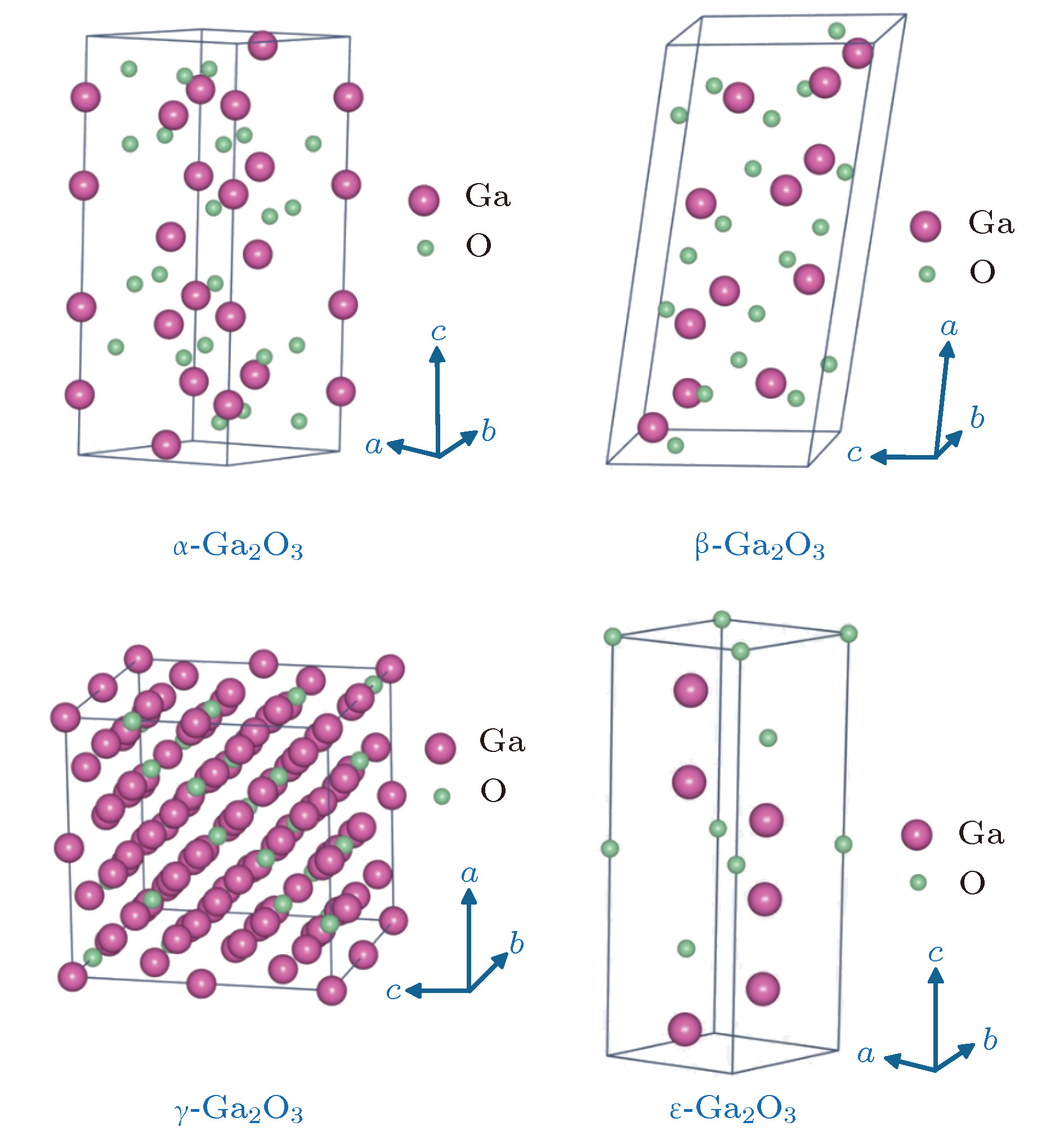
图 1 Ga2O3几个同分异构体的晶体结构
Figure 1. Crystal structures of several isomers of Ga2O3
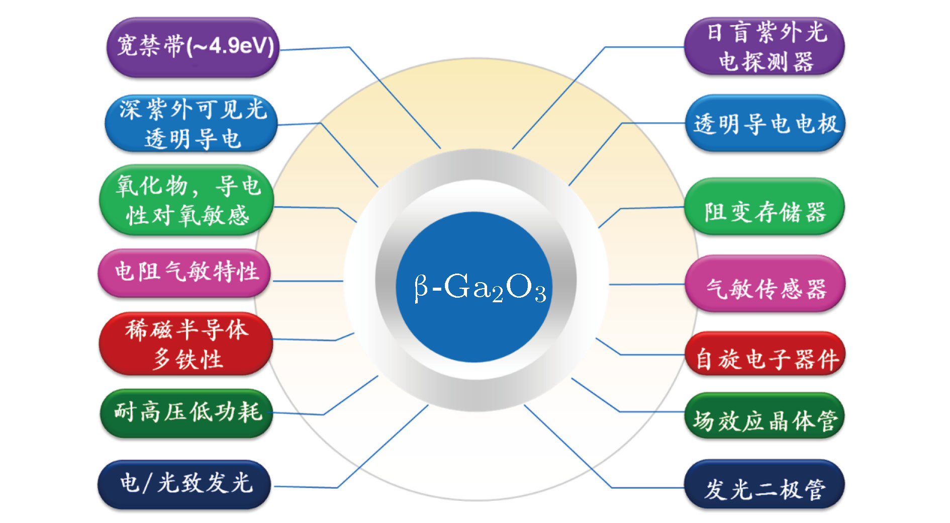
图 4 β-Ga2O3材料具有的物理性质及其对应的器件应用
Figure 4. Physical properties and device applications of β-Ga2O3 material
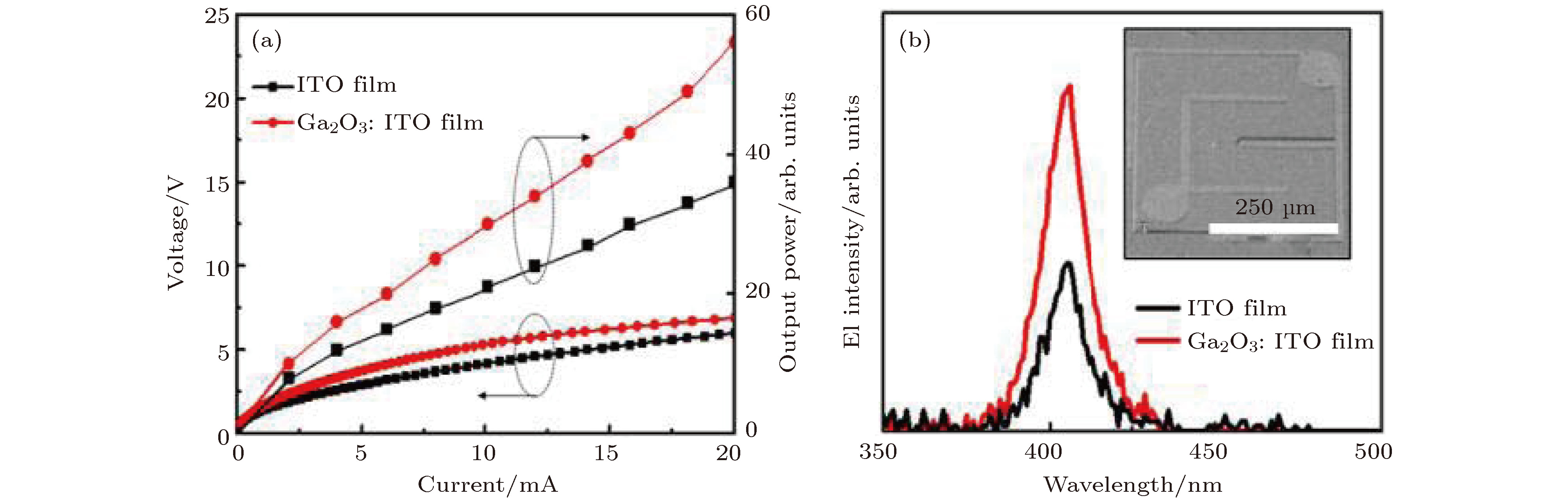
图 7 ITO与Ga2O3:ITO薄膜性能对比 (a)光输出功率–电流–电压特征曲线; (b)近紫外LED的电致发光光谱[85]
Figure 7. (a) Current versus light output power and forward voltage (L-I-V) characteristic curves and (b) typical electroluminescence spectra measured for near-ultraviolet LEDs with Ga2O3:ITO and ITO transparent conducting electrodes; the inset shows top-view SEM image of near-ultraviolet[85]
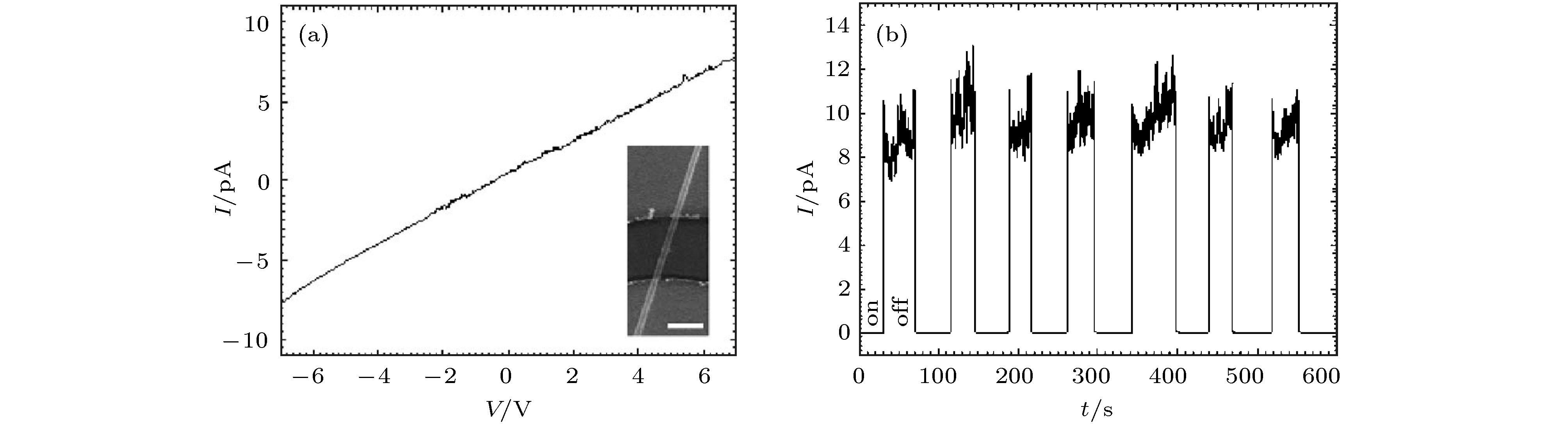
图 8 Au-Ga2O3纳米线-Au光电探测器 (a)黑暗情况下的I–V特性曲线及其器件结构SEM图(插图); (b)–8 V偏压下对254 nm光的I–t响应特性曲线[91]
Figure 8. Au-Ga2O3 nanowire-Au photodetector: (a) I-V characteristic curve of the detector in dark. The inset of is a typical SEM image of the device, the scale bar: 200 nm; (b) real-time photoresponse of the detector to 254 nm light[91]
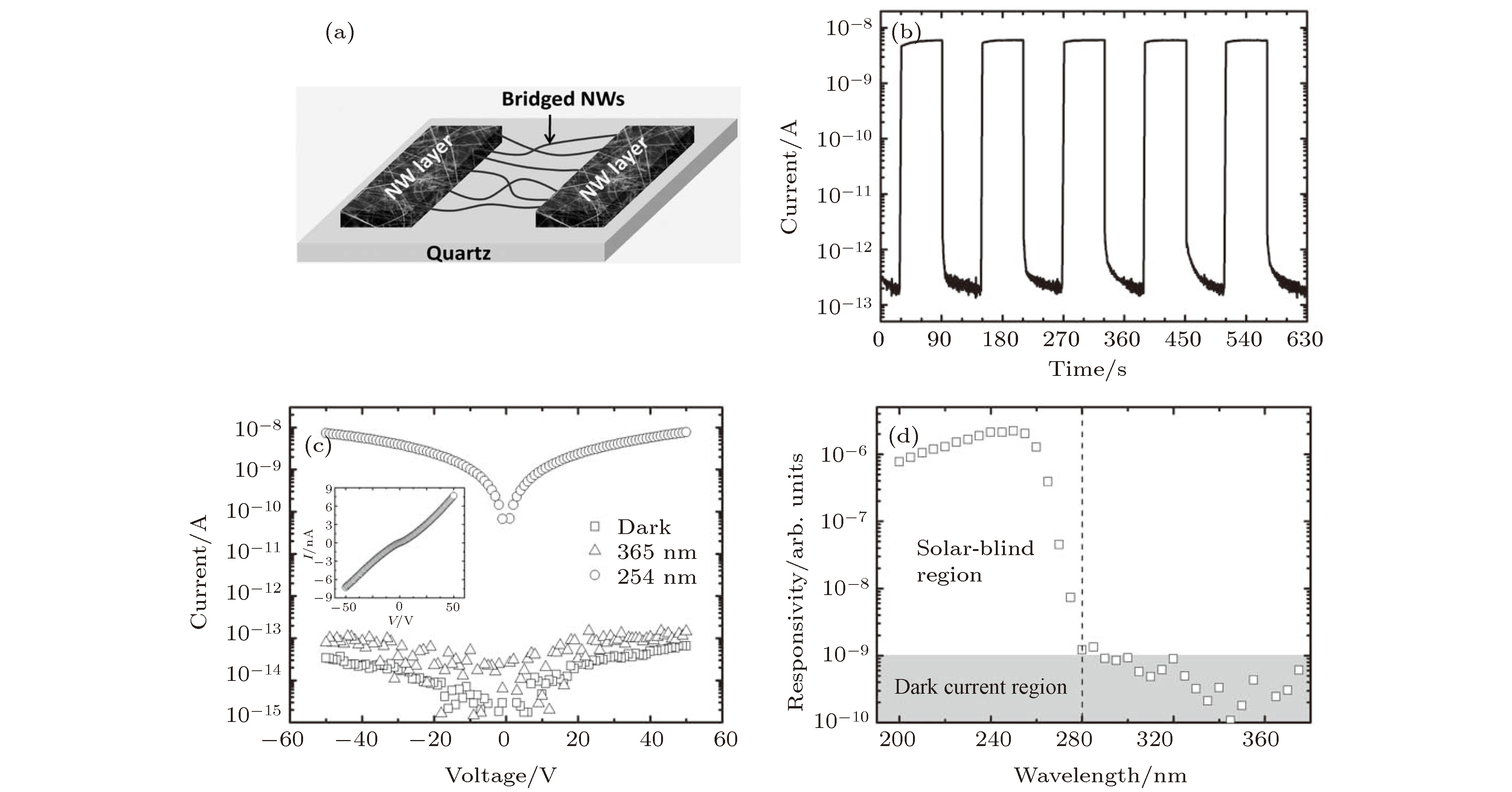
图 9 β-Ga2O3纳米桥光电探测器的日盲光电性质 (a) 器件的结构示意图; (b) 50 V偏压下对254 nm光的I–t响应特性; (c) 黑暗及对365和254 nm光响应的I–V特性曲线; (d) 不同波长的光谱响应特性[88]
Figure 9. Solar blind photoelectric properties of photodetector based on the bridged β-Ga2O3 nanowires: (a) Schematic diagram of the devices; (b) time-dependent photoresponse of the bridged β-Ga2O3 nanowires measured in dry air under UVC (~2 mW cm–2 at 254 nm) illumination with a period of 60 s at a bias voltage of 50 V; (c) I-V characteristics of the bridged β-Ga2O3 nanowires in dark (squares), under 365 nm light (triangles), and under 254 nm light (circles). The I-V curve measured under 254 nm light is plotted on a linear scale in the inset; (d) spectral response of the bridged β-Ga2O3 nanowires revealing that the device is blind to solar light. The dashed line indicates the lowest wavelength of the solar spectrum on Earth[88]

图 10 (a) Ga2O3纳米线光电探测器在不同偏压下的光谱响应[92]; (b)在Cr/Au电极上生长获得的Ga2O3纳米线光电探测器结构[93]; (c)不同温度下生长的Ga2O3纳米线对255 nm光的I–t响应曲线[93]; (d)不同偏压下的光谱响应[93]
Figure 10. (a) Room-temperature spectral responses of the Ga2O3 nanowires photodetector measured with different applied biases[92]; (b) Ga2O3 nanowire photodetector with Cr/Au as electrodes[93]; (c) transit responses measured from the three fabricated photodetectors grown at different temperatures[93]; (d) room-temperature spectral responses of the photodetector under different bias[93]
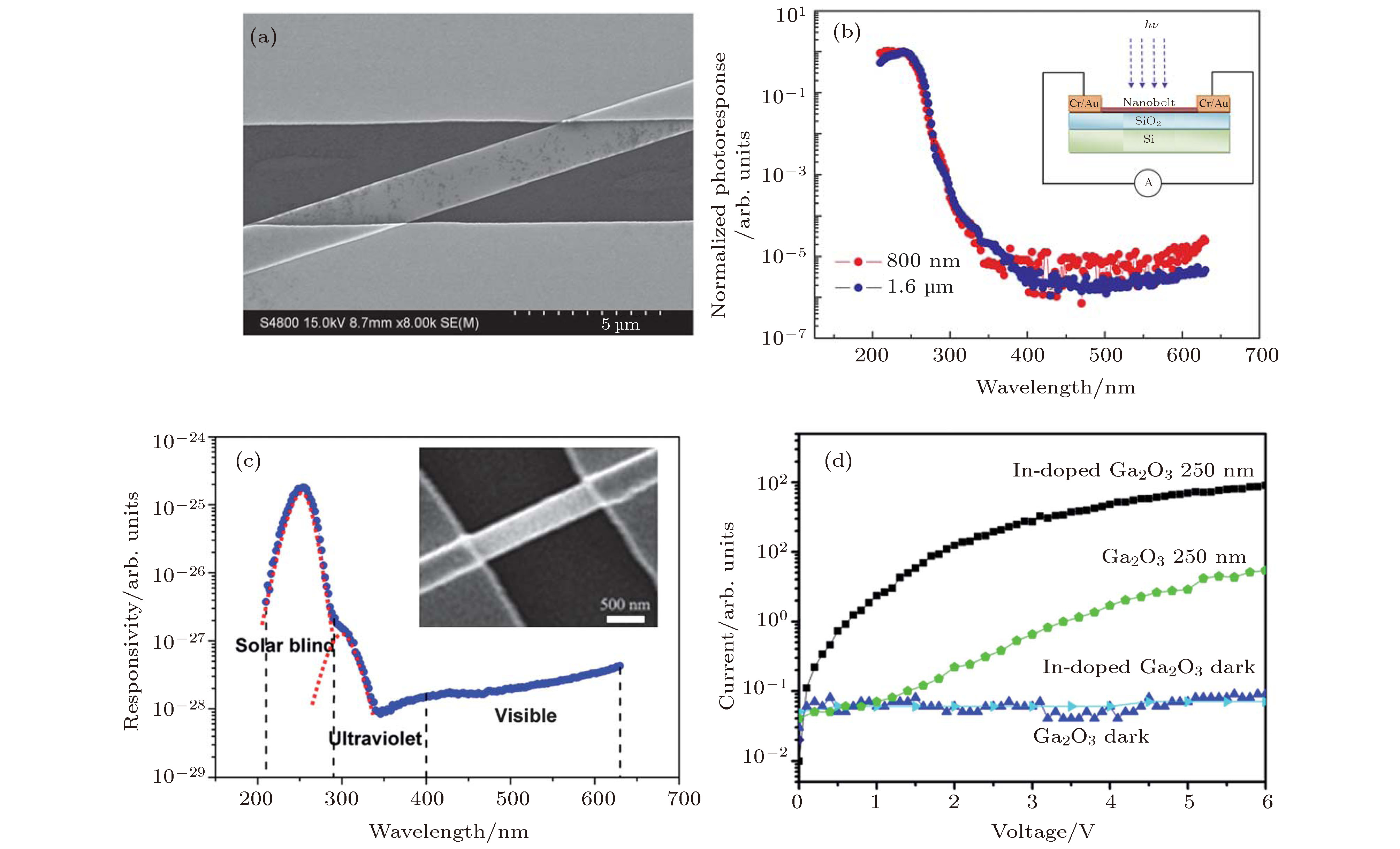
图 11 (a)单条Ga2O3纳米带光电探测器的SEM图[94]; (b)不同带宽Ga2O3纳米带的光谱响应, 插图为探测器结构[94]; (c) In掺杂的Ga2O3单条纳米带光电探测器的光谱响应[95]; (d)纯Ga2O3和In:Ga2O3单条纳米带黑暗情况及在250 nm光照下的I–V曲线[95]
Figure 11. (a) SEM image of a Ga2O3 individual-nanobelt device[94]; (b) spectral response of the devices (nanobelts with different widths of 800 nm and 1.6 mm) measured at a bias of 15 V. The schematic configuration of a photoconductive measurement is inserted in the top-right corner[94]; (c) spectral response of an individual In-doped Ga2O3 nanobelt photodetector. The inset is a typical SEM image of an individual In-doped Ga2O3 nanobelt device[95]; (d) logarithmic plot of I-V curves of the individual Ga2O3 and In-doped Ga2O3 nanobelt photodetector under illumination with the 250 nm wavelength light and in dark conditions[95]
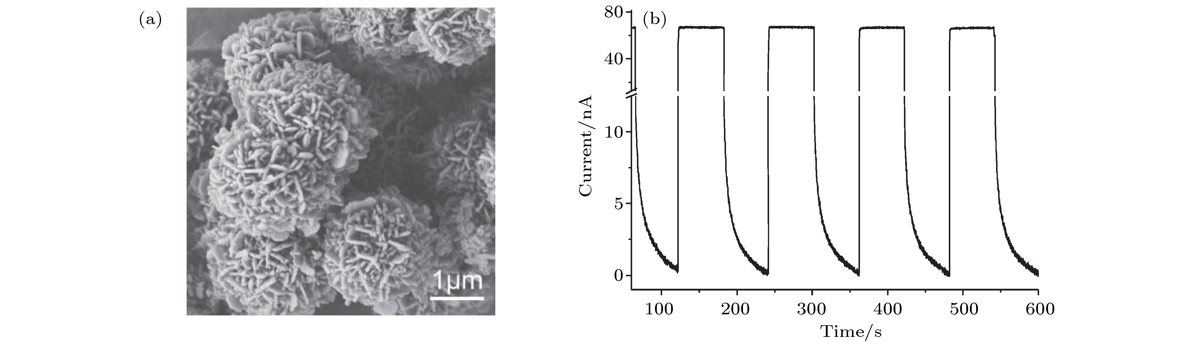
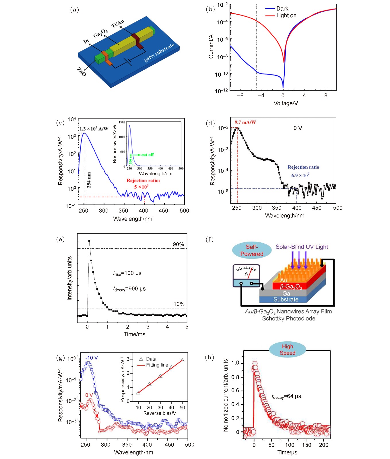
图 13 ZnO/Ga2O3核/壳结构的日盲紫外探测器 (a)器件示意图; (b)黑暗和254 nm光照下的I–V特征曲线; (c)–6 V偏压下的光谱响应[100]; (d)0 V偏压下的光谱响应; (e)光电流衰减[101]. Au/Ga2O3纳米线Schottky型垂直结构的光电探测器 (f)器件示意图; (g)光谱响应; (h)光电流衰减[102]
Figure 13. Solar-blind ultraviolet photodetector based on Single ZnO-Ga2O3 core-shell microwire ZnO/Ga2O3 core-shell: (a) Device schematic diagram; (b)I-V characteristic curve in dark and under 254 nm light; (c) spectral response of the device at −6 V bias[100]; (d) the photoresponse spectrum of the device at 0 V; (e) the time response under the excitation of 266 nm pulse laser at 0 V[101]. Au/Ga2O3 nanowire Schottky vertical structure photodetector: (f) device schematic diagram; (g) spectral responses of the device at zero bias and under reverse bias of 10 V. Inset shows the responsivity of photodetectors at the wavelength of 254 nm as a function of reverse bias; (h) decay edge of the current response at reverse bias of 10 V[102].
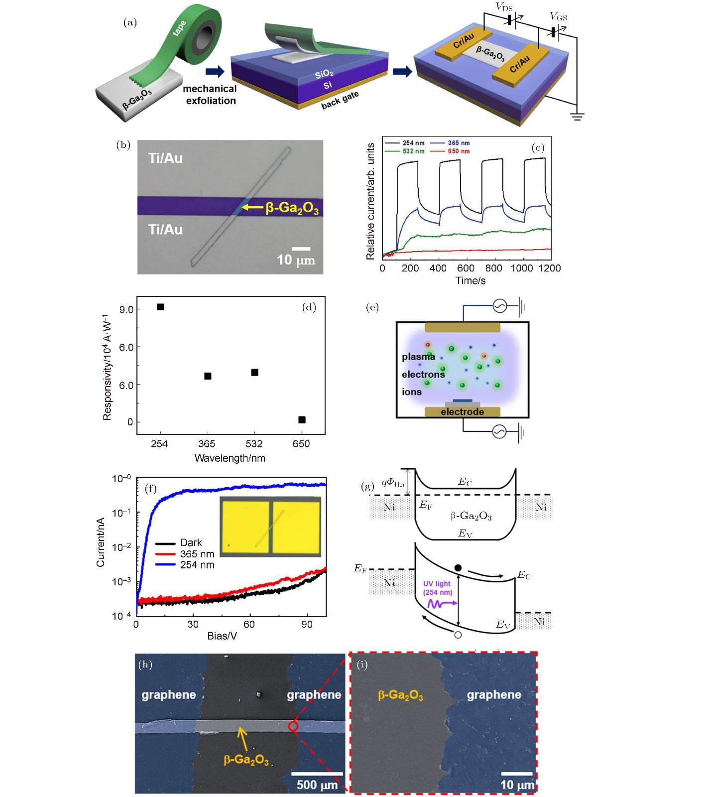
图 14 基于β-Ga2O3薄片的日盲紫外探测器 (a)机械剥离获得β-Ga2O3微米薄片及器件制作流程示意图; (b)器件的光学照片; (c)不同波长光照下的器件的I–t响应曲线; (d) 光谱响应曲线[103]; (e) β-Ga2O3微米薄片的反应离子刻蚀减薄[104]; (f) Ni/Au电极与β-Ga2O3薄片构成的MSM结构肖特基结日盲紫外探测器在不用波长下的I–V曲线; (g)能带结构示意图[105]; (h), (i)石墨烯电极与β-Ga2O3薄片构成的MSM结构日盲紫外探测器的SEM图[106]
Figure 14. Solar-blind ultraviolet photodetector based on β-Ga2O3 flake: (a) Schematic of the entire exfoliated β-Ga2O3 flake based photodetector fabrication process; (b) optical image of the fabricated photodetector; (c) time-dependent photoresponse of the fabricated photodetector under various illumination conditions (254, 365, 532 and 650 nm light exposure); (d) responsivity as a function of wavelength[103]; (e) the reactive ion etching assisted thinning of a β-Ga2O3 flake[104]; (f) the I-V curve; (g) energy band structure diagram of the schottky junction MSM structure solar-blind ultraviolet photodetector based on Ni/Au electrodes and β-Ga2O3 flake under different wavelengths[105]; (h), (i) the SEM image of the MSM structure solar-blind ultraviolet photodetector based on graphene electrode and β-Ga2O3 flake[106]
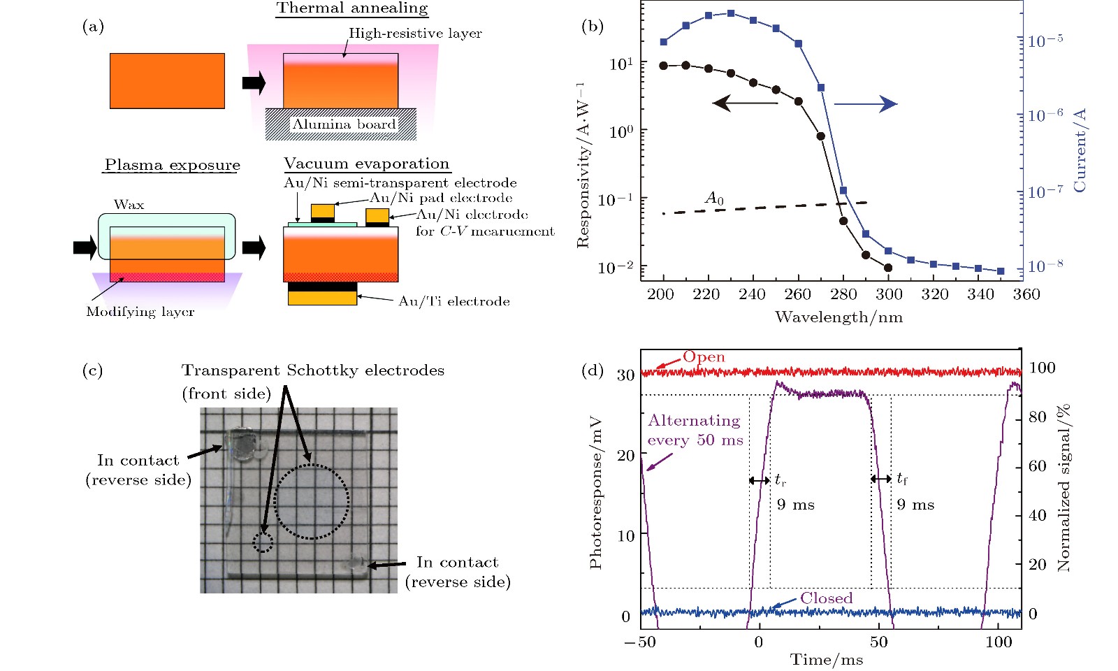
图 15 垂直结构肖特基型β-Ga2O3单晶日盲紫外探测器 (a)制作过程[109]; (b)光谱响应[109]; (c)实物图[89]; (d)瞬态光响应[89]
Figure 15. Vertical solar-blind deep-ultraviolet schottky photodetectors based onβ-Ga2O3 substrates: (a) Fabrication process for photodetector[109]; (b) spectral responser[109]; (c) photograph of the flame detector. The dashed circles are on the edges of the transparent electrodes[89]; (d) transient response of the detector[89]
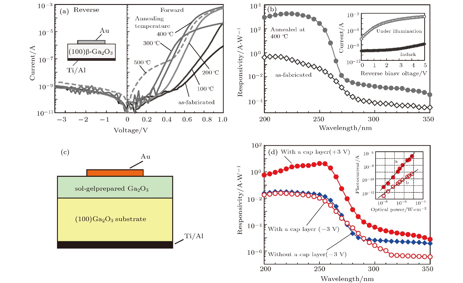
图 16 (a) β-Ga2O3单晶与Au电极在不同温度下退火后的I–V曲线[110]; (b)未退火和400℃下退火后Au/β-Ga2O3单晶肖特基型光电探测器的光谱响应[110]; (c)在β-Ga2O3单晶上采用溶胶凝胶法制备高绝缘β-Ga2O3薄膜并与Au电极构成的光电探测器[111]; (d)有无高绝缘β-Ga2O3薄膜层的光谱响应对比图[111]
Figure 16. (a) Dark I-V characteristics of the Au-Ga2O3 Schottky photodiode annealed at various temperatures. The inset shows the device configuration[110]; (b) spectral response of the Au-Ga2O3 Schottky photodiode before and after annealing at 400℃. The inset shows the reverse I-V characteristics of the photodiode annealed at 400℃ taken in dark and under illumination with 240 nm light[110]; (c) schematic structure of a photodiode composed of a Au Schottky contact and a β-Ga2O3 single-crystal substrate with a sol-gel prepared cap layer.[111]; (d) spectral response of Ga2O3 photodiodes with and without a cap layer at reverse and forward biases of 3 V. The inset shows the incident light intensity dependence of the photocurrent at forward and reverse biases of 3 V under illumination with 250 nm light[111]
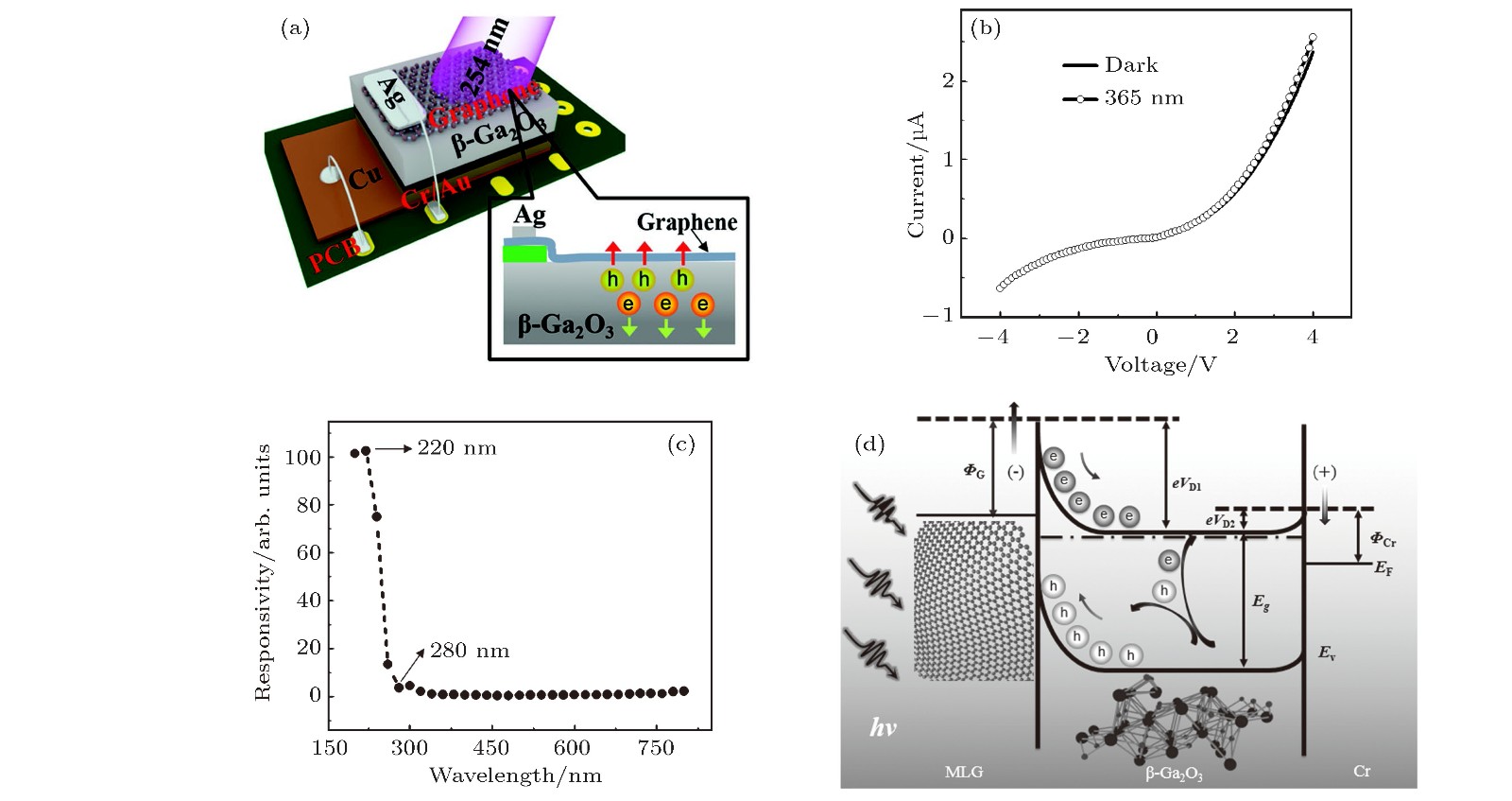
图 17 石墨烯/β-Ga2O3单晶日盲紫外探测器[112] (a)器件结构示意图; (b)黑暗及365 nm光照下的I–V曲线; (c)光谱响应; (d)能带结构示意图
Figure 17. Solar-blind ultraviolet photodetectors based on graphene/β-Ga2O3 single crystal heterojunction[112]: (a) Schematic diagram of device structure; (b) I-V characteristics of the photodetectors in dark and under 365 nm light irradiation; (c) normalized spectral selectivity; (b) energy band diagram at forward bias voltage
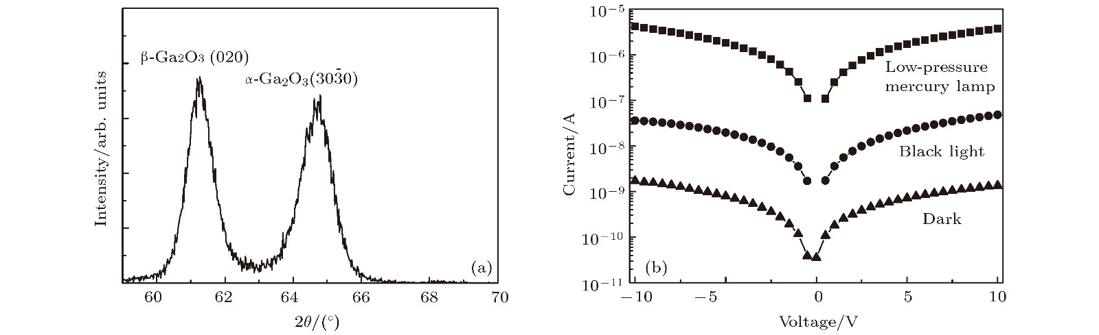
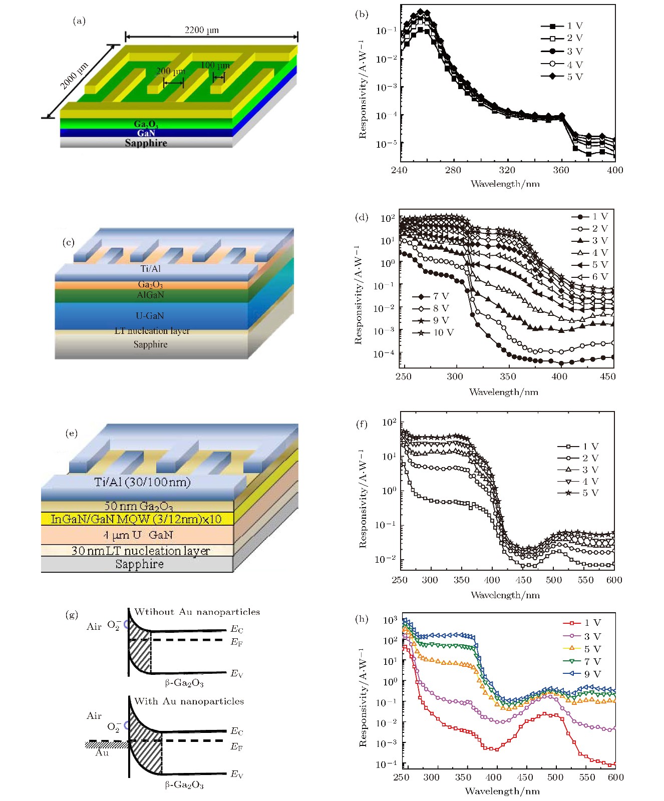
图 19 (a) Ga2O3/GaN光电探测器结构; (b) Ga2O3/GaN光电探测器在不同偏压下的光谱响应[117]; (c) Ga2O3/AlGaN/GaN光电探测器结构; (d) Ga2O3/AlGaN/GaN光电探测器在不同偏压下的光谱响应[118]; (e) Ga2O3/InGaN/GaN光电探测器结构; (f) Ga2O3/InGaN/GaN光电探测器在不同偏压下的光谱响应[119]; (g)有无Au纳米颗粒与Ga2O3界面形成的能带结构示意图; (h) Au纳米颗粒/Ga2O3光电探测器在不同偏压下的光谱响应[120]
Figure 19. Schematic diagram (a) and spectral responses under different bias (b) of Ga2O3/GaN photodetector[117]; Schematic diagram (c) and spectral responses under different bias (d) of Ga2O3/AlGaN/GaN photodetector[118]; Schematic diagram (e) and spectral responses under different bias (f) of Ga2O3/InGaN/GaN photodetector[119]; Energy band diagram of area near the surface of β-Ga2O3 and Au in the dark (g), spectral responses under different bias of Ga2O3/GaN-based metal-semiconductor-metal photodetectors covered with Au nanoparticles (h)[120]
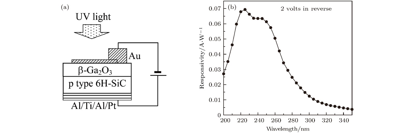
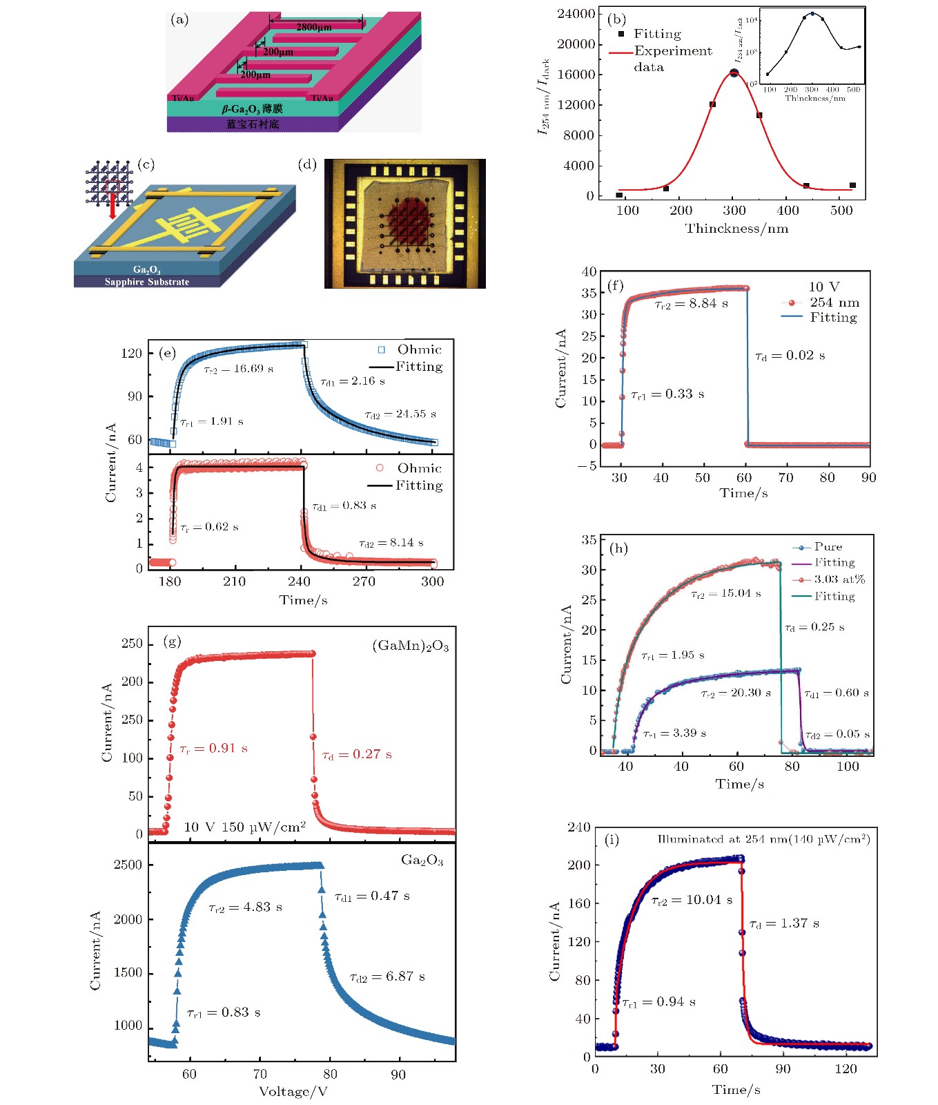
图 21 (a) Ga2O3薄膜MSM结构日盲紫外探测器的结构示意图[123]; (b) MSM结构中Ga2O3薄膜厚度对探测器光暗比的影响[124]; (c), (d) MSM结构阵列探测器[125]; (e)氧气氛退火处理构成的肖特基结与未退火欧姆接触MSM结构探测器的I–t曲线[126]. 不同元素掺杂Ga2O3薄膜MSM结构探测器的I–t曲线 (f) Mg掺杂[128]; (g) Mn掺杂[127]; (h) Zn掺杂[129]; (i) Sn掺杂[130]
Figure 21. (a) Schematic diagram of the β-Ga2O3 thin film MSM structure photodetector[123; (b) the effect of Ga2O3 film thickness on light-dark ratio of the MSM structure photodetector[124]; (c), (d) MSM structure arrays photodetector[125]; (e)I-t curves of the β-Ga2O3 thin films MSM structure photodetector with unannealed (Ohmic-type up) and annealed treatment in O2 atmosphere (Schottky-type, down), respectively[126]. I-t curves of the MSM structure photodetector based on β-Ga2O3 thin films doped with different element: (f) Mg doped[128]; (g) Mn doped[127]; (h) Zn doped[129]; (i) Sn doped[130]
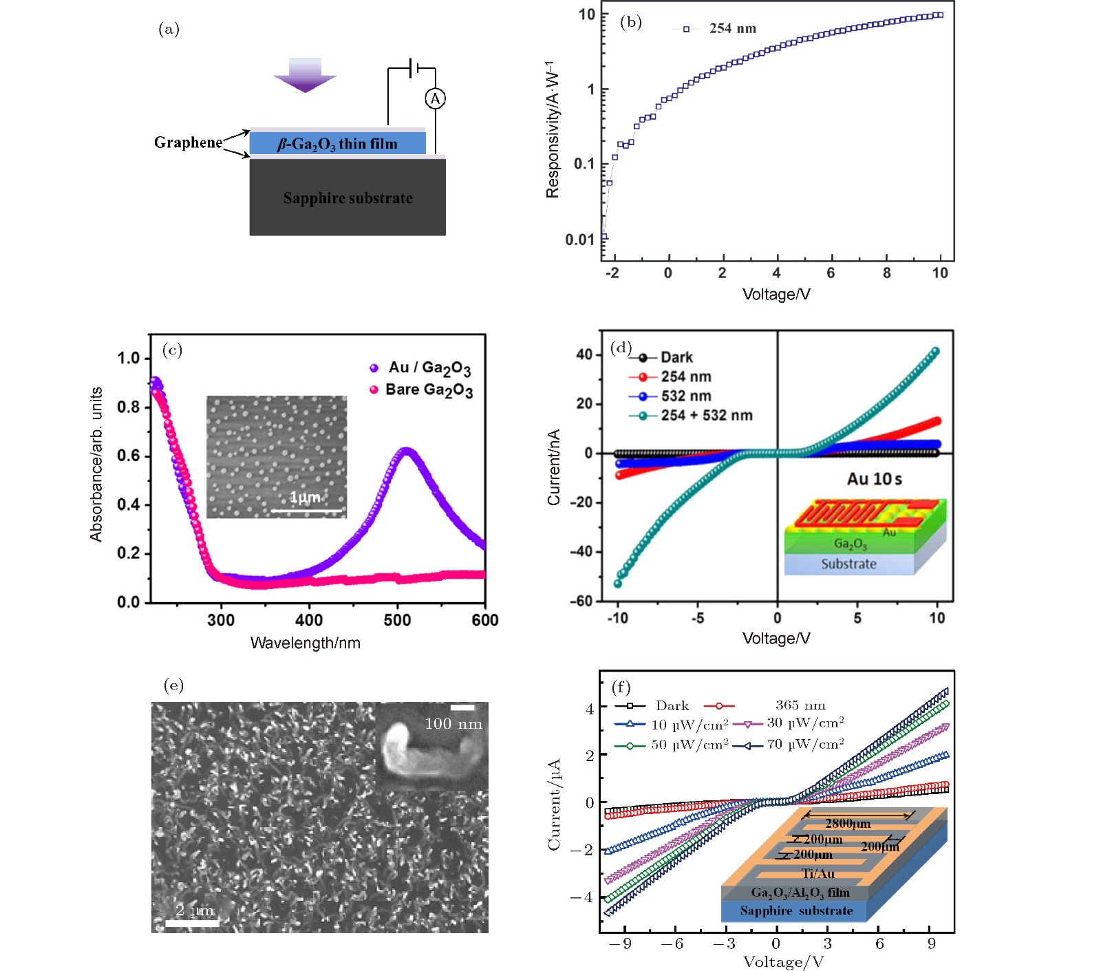
图 22 石墨烯/Ga2O3/石墨烯垂直结构日盲紫外探测器的结构示意图[138](a)及其不同偏压下对254 nm紫外光的响应度(b)[138]; 纯Ga2O3及表面附着有Au纳米颗粒Ga2O3薄膜的紫外可见吸收(c)[139]和不同光照下的I–V曲线(d)[139]; 引入Al2O3薄层生长获得的Ga2O3薄膜/纳米线SEM图(e)[140]和不同光照下的I–V曲线(f)[140]
Figure 22. Schematic diagram (a) [138] and photoresponses to 254 nm ultraviolet light under different bias (b) [138] of graphene/Ga2O3/graphene vertical structure photodetector; UV-vis absorbance spectrum (c) [139] and I-V cures under the different wavelength light illumination (d) [139] of the bare Ga2O3 thin film and Au nanoparticles/Ga2O3 composite thin film; SEM image (e) and I-V cures under the different wavelength light illumination (f) [140] of Ga2O3 thin film/nanowire grown induced by Al2O3 thin layer[140]
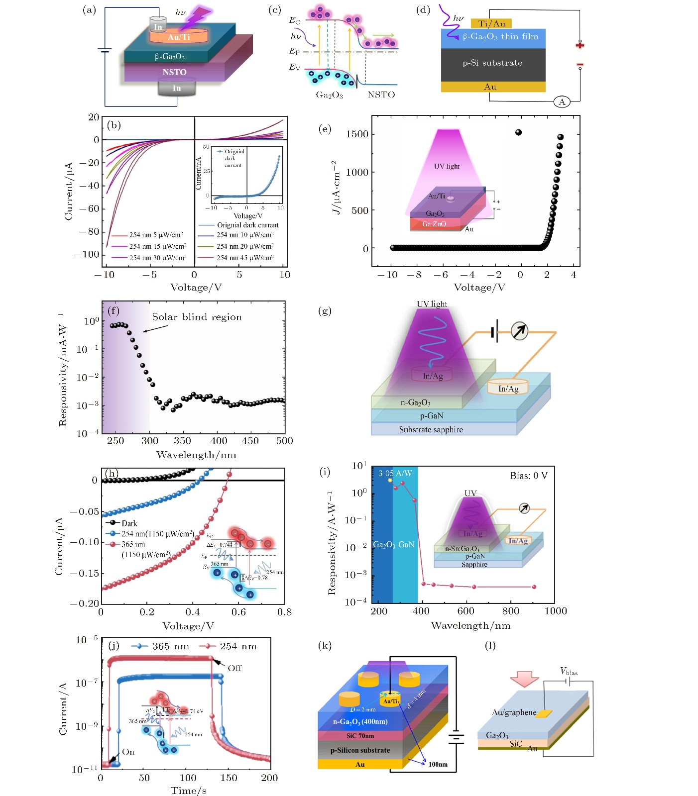
图 23 Ga2O3/NSTO异质结自供电探测器的结构示意图(a)[142] 、黑暗及254 nm不同光强下的I–V曲线(b)[142]和异质结界面处光生载流子输运的能带结构示意图(c)[142]; Ga2O3/P-Si PN结探测器的结构示意图(d)[143]; Ga2O3/Ga:ZnO异质结探测器的整流特性及结构示意图(e)[145]和光谱响应(f)[145]; Ga2O3/GaN PN结探测器的结构示意图(g)[146]和黑暗及不同波长光照下的I–V曲线(h)[146]; Sn:Ga2O3/GaN PN结探测器的光谱响应(i)[144]和不同波长光照下的I–t曲线(j)[147]; Ga2O3/SiC/P-Si PIN结(k)[148]和石墨烯/Ga2O3/SiC探测器的结构示意图(l)[149]
Figure 23. Schematic diagram (a) [142], I-V cures in dark and under 254 nm with different light intensity illumination (b) [142], and schematic energy band diagrams (c) [142] of the β-Ga2O3/NSTO heterojunction self-powered photodetector; Schematic diagram of Ga2O3/P-Si PN junction detector (d) [143]; Rectifier features (e), schematic diagram (e) and spectral response (f) of the Ga2O3/Ga:ZnO heterojunction photodetector[145]; Schematic diagram (g) [145], I-V cures in dark and under the different wavelength light illumination (h) [146]; Spectral response (i) and I-t cures under the different wavelength light illumination (j) of the Sn:Ga2O3/GaN PN junction photodetector[145]; Schematic diagram of Ga2O3/SiC/P-Si PIN junction photodetector (k) [148]and graphene/Ga2O3/SiC photodetector (l)[149]
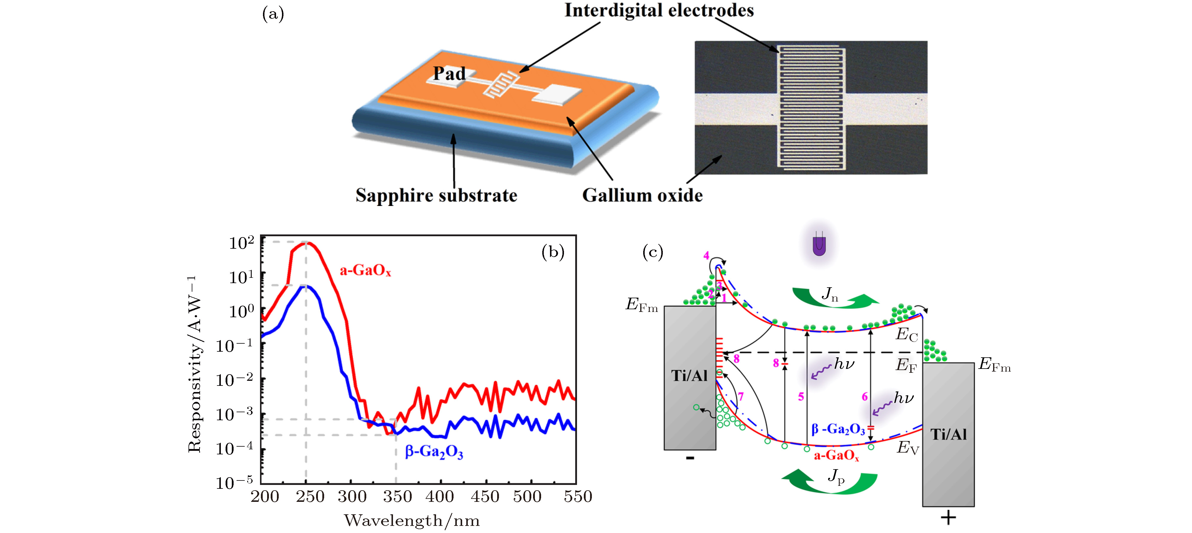
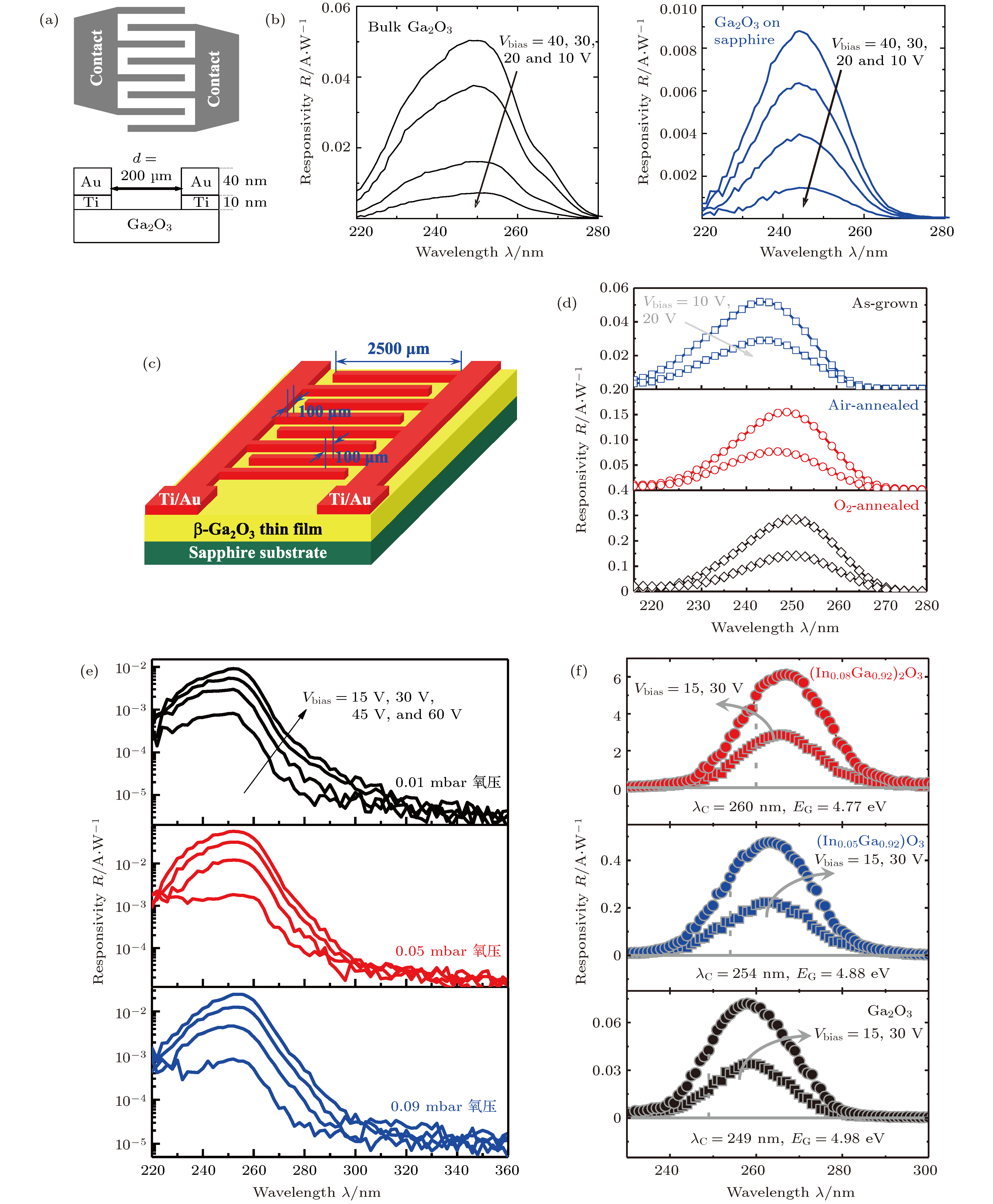
图 25 MSM结构日盲紫外探测器 (a) MSM结构示意图[160]; (b) Ga2O3单晶和薄膜的光谱响应对比[160]; (c) MSM结构[162]; (d) Ga2O3薄膜不同气氛退火的光谱响应对比[161]; (e)不同氧压下生长的Ga2O3薄膜的光谱响应对比[162]; (f)不同In掺杂的Ga2O3薄膜的光谱响应对比图[163]
Figure 25. MSM structure solar-blind ultraviolet photodetector: (a) Schematic diagram of MSM structure[160]; (b) spectral response comparison of Ga2O3 single crystal and thin film[160]; (c) MSM structure[162]; (d) spectral response comparison of Ga2O3 thin films annealed in different atmospheres[161]; (e) spectral response comparison of Ga2O3 thin films grown under different oxygen pressures[162]; (f) spectral response comparison of Ga2O3 thin films doped with different concentrations of In elements[163]

图 26 a-Ga2O3非晶薄膜日盲紫外探测器[169] (a)以石英为衬底的器件结构示意图; (b)光谱响应; (c)光衰减测试; (d)以柔性为衬底的器件结构示意图
Figure 26. Solar-blind ultraviolet photodetector based on a-Ga2O3 amorphous film[169]: (a) Schematic diagram of device structure with quartz substrate; (b) spectral response; (c) the decay of photoresponse; (d) schematic diagram of device structure with flexible substrate
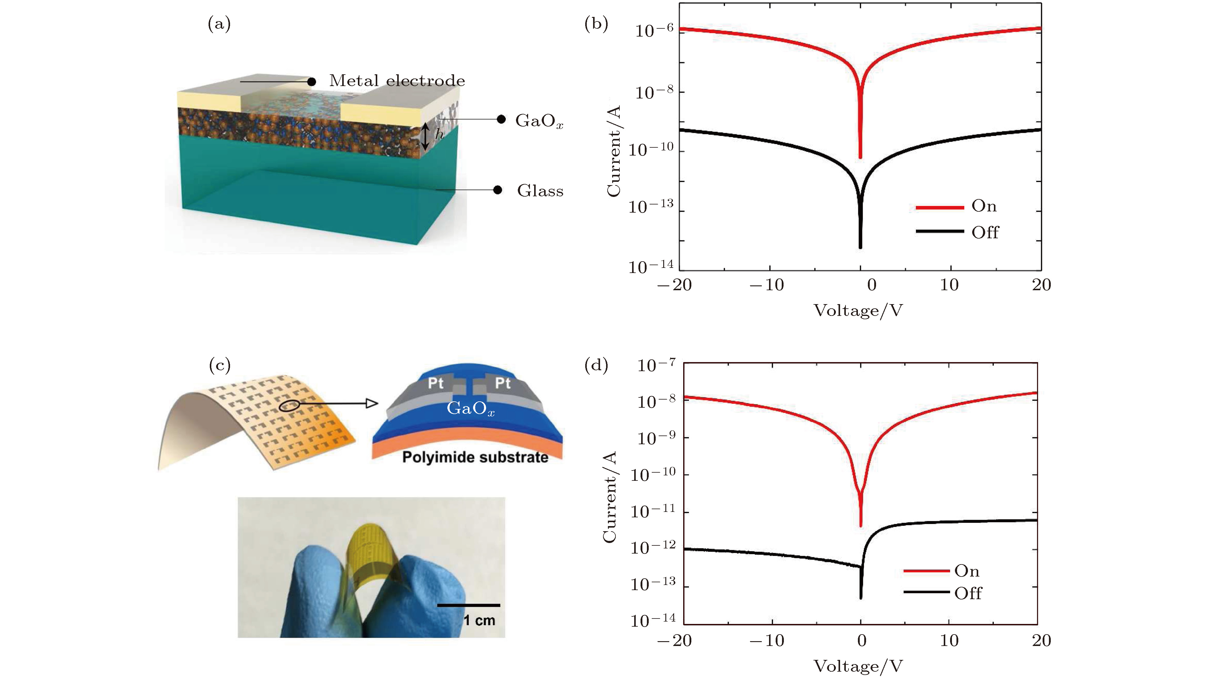
图 27 a-GaOx非晶薄膜日盲紫外探测器[171] (a)以玻璃为衬底的器件结构示意图; (b)黑暗和253 nm光照下的I–V曲线; 以聚酰亚胺为衬底的器件结构示意图(c)及黑暗和253 nm光照下的I–V曲线(d)
Figure 27. Solar-blind ultraviolet photodetector based on a-Ga2O3 amorphous film[171]: Schematic diagram of device structure with glass substrate (a) and I-V cures in dark and under the illumination of 253 nm light (b); Schematic diagram of device structure with polyimide substrate (c) and I-V cures in dark and under the illumination of 253 nm light (d)
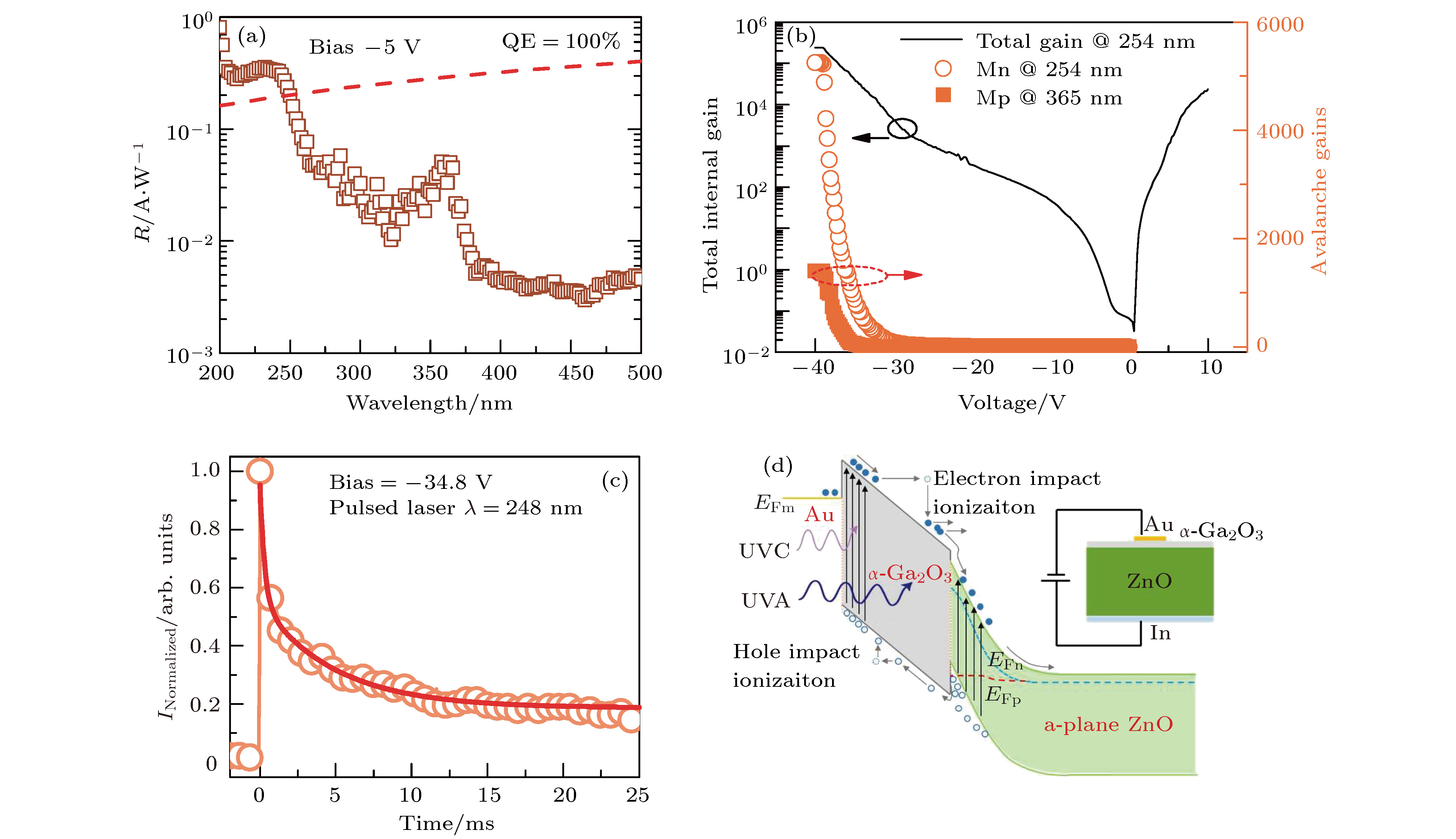
图 28 α-Ga2O3/ZnO异质结日盲紫外探测器[172] (a)光谱响应; (b)增益随偏压的变化; (c)瞬态光响应特性; (d)能带结构及器件结构示意图
Figure 28. Solar-blind ultraviolet photodetector based on α-Ga2O3/ZnO heterojunction[172] : (a) Spectral response; (b) variation of gain with bias; (c) transient photoresponse characteristics; (d) schematic diagram of energy band structure and device structure

图 29 以N2O为反应气体获得的β-Ga2O3薄膜日盲紫外探测器 (a)生长原理示意图[176]; (b)黑暗和255 nm光照下的I–V曲线及MSM结构示意图[176]; (c)光谱响应及不同偏压下的光响应度[176]; (d)石墨烯/β-Ga2O3/GaN器件结构示意图[177]; (e)光谱响应[177]; (f)能带结构示意图[177]
Figure 29. Solar-blind ultraviolet photodetector based on β-Ga2O3 thin film grown using N2O as the reaction gas: (a) Schematic diagram of growth principle[176]; (b) I-V cures in dark and under 255 nm light illumination, and schematic diagram of MSM structure[176]; (c) spectral response and photoresponsivity under different bias[176]; (d) schematic diagram of graphene/β-Ga2O3/GaN devices[177]; (e) spectral response[177]; (f) energy band structure diagram[177]
表 1 β-Ga2O3与主流半导体材料的基本物性比较[25]
Table 1. Comparison of basic physical properties of β-Ga2O3 with mainstream semiconductor materials[25]
材料 Si GaAs GaP 4H-SiC ZnO GaN ß-Ga2O3 Diamond AlN MgO 带隙Eg/eV 1.1 1.43 2.27 3.3 3.35 3.4 4.2—4.9 5.5 6.2 7.8 迁移率${\text{μ}}$/cm2·Vs–1 1400 8500 350 1000 200 1200 300 2000 135 击穿电场强度Eb/MV·cm–1 0.3 0.6 1.0 2.5 3.3 8 10 2 相对介电常数ε 11.8 12.9 11.1 9.7 8.7 9 10 5.5 8.5 9.9 导热率/W·cm–1·K–1 1.5 0.55 1.1 2.7 0.6 2.1 0.23[010] 0.13[100] 10 3.2 巴利加优值/$\varepsilon {\text{μ}} {E_{\rm{b}}}^3$ 1 15 340 870 3444 24664  DownLoad: CSV
表 2 Ga2O3基透明导电电极薄膜的各参数指标汇总
Table 2. Parameters and indicators of Ga2O3-based transparent conductive electrode films
薄膜类型 电导率/S·cm–1 面电阻/Ω·sq–1 载流子浓度/cm–3 迁移率/cm2·V–1·s–1 透过率/% 参考文献 Ga2O3薄膜 7.6 - - - 85 [80] Sn:Ga2O3薄膜 1 - 1.4 × 10¹⁹ 0.44 80 [78] Sn:Ga2O3薄膜 8.2 - - < 0.44 80 [24] Sn:Ga2O3薄膜 8.3 - - 12.03 85 [81] Sn:Ga2O3薄膜 32.3 - 2.4 × 10²⁰ 0.74 88 [82] Sn:Ga2O3单晶 23.4 - 2.3 × 10¹⁸ 64.7 85 [79] (Ga, In)2O3薄膜 1.72 × 10³ - 5 × 10²⁰ - > 95 [83] Ga2O3/ITO薄膜 - 164 - - > 94 [84] Ga2O3/ITO薄膜 - 49 - - 93.8 [85] Ag/Ga2O3薄膜 - 42 - - 91 [86] Ga2O3/Cu/ITO - 50 - - 86 [87]
DownLoad: CSV
表 3 几种无线通信的比较
Table 3. Comparison of several wireless communications
通信类别 非视距通信 抗干扰、防窃听 相对运动信号接收 传播距离调控 受环境气候时间影响 无线电通信 是 易被干扰和窃听 是 很差 受环境影响 激光通信 否 抗干扰、防窃听 否 较差 受环境影响 红外通信 否 较易干扰、防窃听 否 较差 受环境时间影响 紫外通信 是 抗干扰、防窃听 是 很好 很小、全天候
DownLoad: CSV
表 4 Ga2O3基日盲紫外探测器的各参数指标汇总
Table 4. Summary of parameters and indicators of Ga2O3 based solar-blind ultraviolet photodetector.
光电探测器类型 光响应度/A·W–1 量子效率/% 暗电流/A 光暗比 响应时间/s 参考文献 Ga2O3纳米线 - - 10–12 ≈ 2 × 10³ 2.2 × 10⁻¹ [91] Ga2O3纳米线 - - < 10–12 3 × 10⁴ < 2 × 10⁻² [88] Ga2O3纳米线 8.0 × 10⁻⁴ 0.39 2.4 × 10⁻¹⁰ ≈ 102 - [92] Ga2O3纳米线 3.4 × 10⁻³ 1.37 - ≈ 102 - [93] ZnO/Ga2O3核壳微米线 1.3 × 10³(–6 V) - 10–10 ≈ 106 2 × 10⁻⁵ [100] ZnO/Ga2O3核壳微米线 9.7 × 10⁻³(0 V) - 10–10 ≈ 7 × 10² 10–4 [101] Ga2O3纳米线 6 × 10⁻⁴ - 10–11 ≈ 102 6.4 × 10⁻⁵ [102] Ga2O3纳米线 3.77 × 10² 2.0 × 10⁵ 10–11 103 0.21 [107] 石墨烯/Ga2O3纳米线 1.85 × 10⁻¹ - 10–5 - 8 × 10⁻³ [108] Ga2O3纳米片 3.3 1.6 × 10³ 10–9 10 3 × 10⁻² [96] Ga2O3纳米花(γ) - - 10–9 2.2 × 10² 10–1 [97] Ga2O3纳米带 3.37 × 101 1.67 × 10⁴ 10–13 4.0 × 10² 8.6 × 101 [94] Ga2O3纳米带 8.51 × 10² 4.2 × 10³ 10–13 ≈ 103 < 3 × 10⁻¹ [98] Ga2O3纳米带 1.93 × 101 9.4 × 10³ 10–10 ≈ 104 < 2 × 10⁻² [99] In:Ga2O3纳米带 5.47 × 10² 2.72 × 10⁵ 10–13 9.1 × 10² 1 [95] Ga2O3微米带 1.8 × 10⁵(–30 V) 8.8 × 10⁵ 10–6 2.57 0.67 [103] Ga2O3微米带 - - 10–4 - 1.4 [104] Ga2O3微米带 1.68 - 10–13 1.9 × 10³ 0.53 [105] 石墨烯/Ga2O3微米带 2.98 × 101 - 10–13 ≈ 104 - [106] Ga2O3单晶 2.6—8.7 - 10–10 ≈ 103 - [109] Ga2O3单晶 3.7 × 10⁻² 1.8 × 101 10–10 1.5 × 10⁴ 9 × 10⁻³ [89] Ga2O3单晶 103 - 10–10 ≈ 106 - [110] Ga2O3单晶 4.3 2.1 × 101 10–11 105 - [111] 石墨烯/Ga2O3单晶 3.93 × 101 1.96 × 10⁴ 10–6 103 2.2 × 10² [112] Ga2O3单晶 5 × 10⁻² - 10–5 102 2.4 × 10⁻¹ [160] Ga2O3单晶 3 × 10⁻³ - 10–8 101 1.4 × 10⁻¹ [113] Ga2O3薄膜 8 × 10⁻⁵ - - - - [116] Ga2O3薄膜 3.7 × 10⁻² 1.8 × 101 10–9 - - [90] Ga2O3薄膜 4.53 × 10⁻¹ > 102 10–10 105 - [117] Ga2O3薄膜 ≈ 101 - 10–10 103 - [118] Ga2O3薄膜 ≈ 101 - 10–7 103 - [119] Ga2O3薄膜 ≈ 102 - 10–10 102 - [120] Ga2O3薄膜 - - 10–11 105 - [122] Ga2O3薄膜 7.6 × 10⁻¹ - 10–10 6 5 × 10⁻² [152] Ga2O3薄膜 1.7 × 101 8.2 × 10³ 10–9 8.5 × 10⁶ - [153] Ga2O3薄膜 - - 10–11 102 8 × 10⁻¹ [154] Ga2O3薄膜 9.03 × 10⁻¹ - 10–11 105 - [155] Ga2O3薄膜 2.59 × 10² 7.9 × 10⁴ 10–10 104 4 × 10⁻¹ [156] Ga2O3薄膜 - - 10–7 15 - [157] Ga2O3薄膜/晶体 1.8 8.7 × 10² 10–6 36.9 - [158] a-GaOx非晶薄膜 7.0 × 101 - 10–10 1.2 × 10⁵ 2 × 10⁻² [159] Ga2O3薄膜 4.2 - 10–11 1.6 × 10⁴ 4 × 10⁻² [159] Ga2O3薄膜 9 × 10⁻³ - 10–5 101 1.8 × 10⁻¹ [160] Al:Ga2O3薄膜 1.5 7.8 × 10² - - - [164] Si:Ga2O3薄膜 6 × 101 3 × 10⁴ - 9 - [166] Si:Ga2O3薄膜 3.6 × 101 1.75 × 10⁴ - 9 - [167] Zn:Ga2O3薄膜 2.1 × 10² - 10–11 5 × 10⁴ 1.4 [168] Ga2O3非晶薄膜 1.9 × 10⁻¹ - 10–12 106 1.9 × 10⁻⁵ [169] Ga2O3非晶薄膜 4.5 × 101 - 10–10 104 2.97 × 10⁻⁶ [171] Ga2O3薄膜 1.5 - 10–9 103 - [175] Ga2O3薄膜 0.29 1.34 10–8 1.6 × 10³ 0.1 [173] Ga2O3薄膜 0.11 - 10–9 3.5 × 10³ 0.45 [174] Ga2O3薄膜 0.14 - 10–11 1.4 × 10⁶ 0.2 [174] Ga2O3薄膜 1.5 - 10–8 103 - [173] Ga2O3薄膜 2.6 × 101 - 10–8 104 0.18 [176] 石墨烯/Ga2O3薄膜 1.28 × 101 - 10–8 - 2 × 10⁻³ [177] Ga2O3薄膜 9.6 × 101 4.76 × 10⁴ 10–6 - - [180] Ga2O3薄膜 5.86 × 10⁻⁵ - 10–9 1.8 × 101 0.1 [181] Ga2O3薄膜 1.5 × 10² 7 × 10⁴ 10–11 105 1.3 [165] Ga2O3薄膜 1 × 10⁻¹ - 10–8 - - [178] Ga2O3薄膜 - - 10–8 6 8.6 × 10⁻¹ [123] Ga2O3薄膜 - - 10–9 1.3 × 101 6.2 × 10⁻¹ [126] Ga2O3/Ga/Ga2O3薄膜 2.854 - 10–11 8 × 10⁵ - [170] Mn:Ga2O3薄膜 7 × 10⁻² 3.6 × 101 10–9 6.7 × 101 2.8 × 10⁻¹ [127] α-Ga2O3薄膜 1.5 × 10⁻² 7.39 10–9 3 × 101 - [137] α-Sn:Ga2O3薄膜 9.6 × 10⁻² - 10–9 1.4 × 10² 1.08 [132] α-Sn:Ga2O3薄膜 - - 10–7 4 8.73 [131] ε-Sn:Ga2O3薄膜 6.05 × 10⁻³ 3.02 10–9 46.46 - [133] β-Sn:Ga2O3薄膜 3.61 × 10⁻² - 10–8 19 1.37 [166] Zn:Ga2O3薄膜 - - 10–9 2 1.23 [134] Er:Ga2O3薄膜 - - 10–9 2.5 1.6 × 10⁻¹ [76] Au NPs/Ga2O3薄膜 102 - 10–6 > 2 × 10² - [139] Ga2O3/p-Si异质结 3.7 × 10² 1.8 × 10⁵ 10–8 9.4 × 10² 1.8 [143] Ga2O3/ZnO异质结 3.5 × 10⁻¹ 1.7 × 10² 10–10 1.5 × 101 6.2 × 10⁻¹ [144] Ga2O3/NSTO异质结 4.3 × 101 2.1 × 10⁴ 10–6 2 × 101 7 × 10⁻² [142] Ga2O3/Ga:ZnO异质结 7.6 × 10⁻⁴ - 10–9 2.6 × 10² 2.7 × 10⁻¹ [145] p-Si/i-SiC/n-Ga2O3 - - 10–8 5.4 × 10³ - [148] 石墨烯/Ga2O3/SiC 1.8 × 10⁻¹ - 10–5 6.3 × 101 1.7 [149] 石墨烯/Ga2O3/石墨烯 9.66 - 10–9 8.3 × 101 0.96 [138] Ga2O3/SiC/Al2O3 - - 10–9 7.7 - [141] Ga2O3/Al2O3 1.4 - 10–7 9.04 1.26 [140] Ga2O3/SiC异质结 7 × 10⁻² - 10–10 - 9 × 10⁻³ [121] Ga2O3/GaN异质结 5.4 × 10⁻² - 10–6 1.5 × 10² 8 × 10⁻² [146] Sn:Ga2O3/GaN异质结 3.05 - 10–11 104 1.8 × 10⁻² [147] α-Ga2O3/ZnO异质结 1.1 × 10⁴(–40 V) - 10–12 - 2.4 × 10⁻⁴ [172] Ga2O3/金刚石异质结 2 × 10⁻⁴ - 10–9 3.7 × 101 - [179]
DownLoad: CSV
-
[1] 程轶 2013 博士学位论文(大连: 大连理工大学)
Cheng Y 2013 Ph. D. Dissertation (Dalian: Dalian University of Technology) (in Chinese)
[2] 马海林, 苏庆 2014 物理学报 63 116701
Google Scholar
Ma H L, Su Q 2014 Acta Phys. Sin. 63 116701
Google Scholar
[3] 潘惠平, 成枫锋, 李琳, 洪瑞华, 姚淑德 2013 物理学报 62 048801
Google Scholar
Pan H P, Cheng F F, Li L, Hong R H, Yao S D 2013 Acta Phys. Sin. 62 048801
Google Scholar
[4] Roy R, Hill V G, Osborn E F 1952 J. Am. Chem. Soc. 74 719
Google Scholar
[5] Kaneko K, Nomura T, Kakeya I, Fujita S 2009 Appl. Phys. Express 2 075501
Google Scholar
[6] Fujita S, Kaneko K 2014 J. Cryst. Growth 401 588
Google Scholar
[7] Shinohara D, Fujita S 2008 Jpn. J. Appl. Phys. 47 7311
Google Scholar
[8] Schewski R, Wagner G, Baldini M, Gogova D, Galazka Z, Schulz T, Remmele T, Markurt T, Wenckstern H V, Grundmann M, Bierwagen O, Vogt P, Albrecht M 2015 Appl. Phys. Express 8 011101
Google Scholar
[9] Lee S D, Akaiwa K, Fujita S 2013 Phys. Status Solidi C 10 1592
Google Scholar
[10] Lee S D, Ito Y, Kaneko K, Fujita S 2015 Jpn. J. Appl. Phys. 54 030301
Google Scholar
[11] Kaneko K, Nomura T, Fujita S 2010 Phys. Status Solidi C 7 2467
Google Scholar
[12] Kaneko K, Kakeya I, Komori S, Fujita S 2013 J. Appl. Phys. 113 233901
Google Scholar
[13] Mitome M, Kohiki S, Nagai T, Kurashima K, Kimoto K, Bando Y 2013 Cryst. Growth Des. 13 3577
Google Scholar
[14] Wang T, Farvid S S, Abulikemu M, Radovanovic P V 2010 J. Am. Chem. Soc. 132 9250
Google Scholar
[15] Playford H Y, Hannon A C, Tucker M G, Dawson D M, Ashbrook S E, Kastiban R J, Sloan J, Walton R I 2014 J. Phys. Chem. C 118 16188
Google Scholar
[16] Lorenzi R, Paleari A, Golubev N V, Ignat'eva E S, Sigaev V N, Niederberger M, Lauria A 2015 J. Mater. Chem. C 3 41
Google Scholar
[17] Takahashi M, Nakatani T, Iwamoto S, Watanabe T, Inoue M 2006 J. Phys. Condens Matter 18 5745
Google Scholar
[18] Oshima Y, Víllora E G, Matsushita Y, Yamamoto S, Shimamura K 2015 J. Appl. Phys. 118 085301
Google Scholar
[19] Ge S X, Zheng Z 2009 Solid State Sci. 11 1592
Google Scholar
[20] Tsuchiya T, Yusa H, Tsuchiya J 2007 Phys. Rev. B 76 174108
Google Scholar
[21] Bermudez V M 2006 Chem. Phys. 323 193
Google Scholar
[22] Yamaga M, Víllora E G, Shimamura K, Ichinose N, Honda M 2003 Phys. Rev. B 68 155207
Google Scholar
[23] Zacherle T, Schmidt P C, Martin M 2013 Phys. Rev. B 87 235206
Google Scholar
[24] Orita M, Hiramatsu H, Ohta H, Hirano M, Hosono H 2002 Thin Solid Films 411 134
Google Scholar
[25] Higashiwaki M, Sasaki K, Kuramata A, Masui T, Yamakoshi S 2012 Appl. Phys. Lett. 100 013504
Google Scholar
[26] Dong L, Jia R, Xin B, Zhang Y 2016 J. Vac. Sci. Technol., A 34 060602
[27] Dong L, Jia R, Xin B, Peng B, Zhang Y 2017 Sci. Rep. 7 40160
Google Scholar
[28] Tao X T 2019 J. Semicond. 40 010401
Google Scholar
[29] Fu B, Jia Z T, Mu W X, Yin Y R, Zhang J, Tao X T 2019 J. Semicond. 40 011804
Google Scholar
[30] Mohamed H F, Xia C T, Sai Q L, Cui H Y, Pan M Y, Qi H J 2019 J. Semicond. 40 011801
Google Scholar
[31] Higashiwaki M, Sasaki K, Murakami H, Kumagai Y, Koukitu A, Kuramata A, Masui T, Yamakoshi S 2016 Semicond. Sci. Technol. 31 034001
Google Scholar
[32] Razeghi M 2002 Proc. IEEE 90 1006
Google Scholar
[33] Du X, Mei Z, Liu Z, Guo Y, Zhang T, Hou Y, Zhang Z, Xue Q, Kuznetsov A Y 2009 Adv. Mater. 21 4625
Google Scholar
[34] Higashiwaki M, Sasaki K, Kuramata A, Masui T, Yamakoshi S 2014 Phys. Status Solidi A 211 21
Google Scholar
[35] Higashiwaki M, Jessen G H 2018 Appl. Phys. Lett. 112 060401
Google Scholar
[36] Villora E G, Arjoca S, Shimamura K, Inomata D, Aoki K 2014 Proc. of SPIE 8987 1
[37] Wellenius P, Suresh A, Foreman J V, Everitt H O, Muth J F 2008 Mater. Sci. Eng. B 146 252
Google Scholar
[38] Wellenius P, Suresh A, Muth J F 2008 Appl. Phys. Lett. 92 021111
Google Scholar
[39] Vanithakumari S C, Nanda K K 2009 Adv. Mater. 21 3581
Google Scholar
[40] Lin C F, Chen K T, Huang K P 2010 IEEE Electron Device Lett. 31 1431
Google Scholar
[41] Choi S E, Oh Y T, Ham H K, Kim T W, Heo G S, Park J W, Choi B H, Shin D C 2011 Curr. Appl. Phys. 11 S255
[42] Iizuka K, Morishima Y, Kuramata A, Shen Y J, Tsai C Y, Su Y Y, Liu G, Hsu T C, Yeh J H 2015 Proc. of SPIE 9363 1
[43] Schwebel T, Fleischer M, Meixner H, Kohl C D 1998 Sens. Actuators B 49 46
Google Scholar
[44] Kohl D, Ochs T, Geyer W, Fleischer M, Meixner H 1999 Sens. Actuators B 59 140
Google Scholar
[45] Ogita M, Saika N, Nakanishi Y, Hatanaka Y 1999 Appl. Surf. Sci. 142 188
Google Scholar
[46] Schwebel T, Fleischer M, Meixner H 2000 Sens. Actuators B 65 176
Google Scholar
[47] Baban C, Toyoda Y, Ogita M 2005 Thin Solid Films 484 369
Google Scholar
[48] Bartic M, Toyoda Y, Baban C I, Ogita M 2006 Jpn. J. Appl. Phys., Part1 45 5186
Google Scholar
[49] Feng P, Xue X Y, Liu Y G, Wan Q, Wang T H 2006 Appl. Phys. Lett. 89 112114
Google Scholar
[50] Bartic M, Baban C I, Suzuki H, Ogita M, Isai M 2007 J. Am. Ceram. Soc. 90 2879
Google Scholar
[51] Liu Z F, Yamazaki T, Shen Y, Kikuta T, Nakatani N, Li Y 2008 Sens. Actuators B 129 666
Google Scholar
[52] Arnold S P, Prokes S M, Perkins F K, Zaghloul M E 2009 Appl. Phys. Lett. 95 103102
Google Scholar
[53] Lee C T, Yan J T 2010 Sens. Actuators B 147 723
Google Scholar
[54] Hou Y, Jayatissa A H 2014 Sens. Actuators B 204 310
Google Scholar
[55] Bartic M 2015 Phys. Status Solidi A 211 40
[56] Hayashi H, Huang R, Ikeno H, Oba F, Yoshioka S, Tanaka I, Sonoda S 2006 Appl. Phys. Lett. 89 181903
Google Scholar
[57] Pei G, Xia C, Dong Y, Wu B, Wang T, Xu J 2008 Scr. Mater. 58 943
Google Scholar
[58] Guo D Y, Wu Z P, An Y H, Li X J, Guo X C, Chu X L, Sun C L, Lei M, Li L H, Cao L X, Li P G, Tang W H 2015 J. Mater. Chem. C 3 1830
Google Scholar
[59] Guo D Y, Wu Z P, Li P G, Wang Q J, Lei M, Li L H, Tang W H 2015 RSC Adv. 5 12894
Google Scholar
[60] Guo D Y, An Y H, Cui W, Zhi Y S, Zhao X L, Lei M, Li L H, Li P G, Wu Z P, Tang W H 2016 Sci. Rep. 6 25166
Google Scholar
[61] Gao X, Xia Y, Ji J, Xu H, Su Y, Li H, Yang C, Guo H, Yin J, Liu Z 2010 Appl. Phys. Lett. 97 193501
Google Scholar
[62] Yang J B, Chang T C, Huang J J, Chen S C, Yang P C, Chen Y T, Tseng H C, Sze S M, Chu A K, Tsai M J 2013 Thin Solid Films 529 200
Google Scholar
[63] Aoki Y, Wiemann C, Feyer V, Kim H S, Schneider C M, Ill-Yoo H, Martin M 2014 Nat. Commun. 5 3473
Google Scholar
[64] Hsu C W, Chou L J 2012 Nano Lett. 12 4247
Google Scholar
[65] Lee D Y, Tseng T Y 2011 J. Appl. Phys. 110 114117
Google Scholar
[66] Huang J J, Chang T C, Yang J B, Chen S C, Yang P C, Chen Y T, Tseng H C, Sze S M, Chu A K, Tsai M J 2012 IEEE Electron Device Lett. 33 1387
Google Scholar
[67] Yang J B, Chang T C, Huang J J, Chen Y T, Yang P C, Tseng H C, Chu A K, Sze S M, Tsai M J 2013 Thin Solid Films 528 26
Google Scholar
[68] Guo D Y, Wu Z P, An Y H, Li P G, Wang P C, Chu X L, Guo X C, Zhi Y S, Lei M, Li L H, Tang W H 2015 Appl. Phys. Lett. 106 042105
Google Scholar
[69] Guo D Y, Wu Z P, Zhang L J, Yang T, Hu Q R, Lei M, Li P G, Li L H, Tang W H 2015 Appl. Phys. Lett. 107 032104
Google Scholar
[70] Guo D Y, Qian Y P, Su Y L, Shi H Z, Li P G, Wu J T, Wang S L, Cui C, Tang W H 2017 AIP Adv. 7 065312
Google Scholar
[71] Wang P C, Li P G, Zhi Y S, Guo D Y, Pan A Q, Zhan J M, Liu H, Shen J Q, Tang W H 2015 Appl. Phys. Lett. 107 262110
Google Scholar
[72] Gollakota P, Dhawan A, Wellenius P, Lunardi L M, Muth J F, Saripalli Y N 2006 Appl. Phys. Lett. 88 221906
Google Scholar
[73] Sawada K, Adachi S 2014 ECS J. Solid State Sci. 3 R238
Google Scholar
[74] Kang B K, Mang S R, Lim H D, Song K M, Song Y H, Go D H, Jung M K, Senthil K, Yoon D H 2014 Mater. Chem. Phys. 147 178
Google Scholar
[75] Wu Z, Bai G, Hu Q, Guo D, Sun C, Ji L, Lei M, Li L, Li P, Hao J, Tang W 2015 Appl. Phys. Lett. 106 171910
Google Scholar
[76] Wu Z, Bai G, Qu Y, Guo D, Li L, Li P, Hao J, Tang W 2016 Appl. Phys. Lett. 108 211903
Google Scholar
[77] Li W, Peng Y, Wang C, Zhao X, Zhi Y, Yan H, Li L, Li P, Yang H, Wu Z, Tang W 2017 J. Alloys Compd. 697 388
Google Scholar
[78] Orita M, Ohta H, Hirano M, Hosono H 2000 Appl. Phys. Lett. 77 4166
Google Scholar
[79] Suzuki N, Ohira S, Tanaka M, Sugawara T, Nakajima K, Shishido T 2007 Phys. Status Solidi C 4 2310
Google Scholar
[80] Ou S L, Wuu D S, Fu Y C, Liu S P, Horng R H, Liu L, Feng Z C 2012 Mater. Chem. Phys. 133 700
Google Scholar
[81] Du X J, Li Z, Luan C N, Wang W G, Wang M X, Feng X J, Xiao H D, Ma J 2015 J. Mater. Sci. 50 3252
Google Scholar
[82] Mi W, Li Z, Luan C N, Xiao H D, Zhao C S, Ma J 2015 Ceram. Int. 41 2572
Google Scholar
[83] Minami T, Takeda Y, Kakumu T, Takata S, Fukuda I 1997 J. Vac. Sci. Technol., A 15 958
Google Scholar
[84] Kim S, Kim S J, Kim K H, Kim H D, Kim T G 2014 Phys. Status Solidi A 211 2569
Google Scholar
[85] Kim S J, Park S Y, Kim K H, Kim S W, Kim T G 2014 IEEE Electron Device Lett. 35 232
Google Scholar
[86] Woo K Y, Lee J H, Kim K H, Kim S J, Kim T G 2014 Phys. Status Solidi A 211 1760
Google Scholar
[87] Zhuang H H, Yan J L, Xu C Y, Meng D L 2014 Appl. Surf. Sci. 307 241
Google Scholar
[88] Li Y, Tokizono T, Liao M, Zhong M, Koide Y, Yamada I, Delaunay J J 2010 Adv. Funct. Mater. 20 3972
Google Scholar
[89] Oshima T, Okuno T, Arai N, Suzuki N, Hino H, Fujita S 2009 Jpn. J. Appl. Phys. 48 011605
Google Scholar
[90] Oshima T, Okuno T, Fujita S 2007 Jpn. J. Appl. Phys. 46 7217
Google Scholar
[91] Feng P, Zhang J Y, Li Q H, Wang T H 2006 Appl. Phys. Lett. 88 153107
Google Scholar
[92] Weng W Y, Hsueh T J, Chang S J, Huang G J, Chang S P 2010 IEEE Photonics Technol. Lett. 22 709
Google Scholar
[93] Wu Y L, Chang S J, Weng W Y, Liu C H, Tsai T Y, Hsu C L, Chen K C 2013 IEEE Sens. J. 13 2368
Google Scholar
[94] Li L, Auer E, Liao M, Fang X, Zhai T, Gautam U K, Lugstein A, Koide Y, Bando Y, Golberg D 2011 Nanoscale 3 1120
Google Scholar
[95] Tian W, Zhi C, Zhai T, Chen S M, Wang X, Liao M Y, Golberg D, Bando Y 2012 J. Mater. Chem. 22 17984
Google Scholar
[96] Feng W, Wang X N, Zhang J, Wang L, Zheng W, Hu P, Cao W, Yang B 2014 J. Mater. Chem. C 2 3254
Google Scholar
[97] Teng Y, Song L X, Ponchel A, Yang Z K, Xia J 2014 Adv. Mater. 26 6238
Google Scholar
[98] Zou R J, Zhang Z Y, Liu Q, Hu J Q, Sang L W, Liao M Y, Zhang W J 2014 Small 10 1848
Google Scholar
[99] Zhong M Z, Wei Z M, Meng X Q, Wu F, Li J 2015 J. Alloys Compd. 619 572
Google Scholar
[100] Zhao B, Wang F, Chen H Y, Wang Y P, Jiang M M, Fang X S, Zhao D X 2015 Nano Lett. 15 3988
Google Scholar
[101] Zhao B, Wang F, Chen H, Zheng L, Su L, Zhao D, Fang X 2017 Adv. Funct. Mater. 27 1700264
Google Scholar
[102] Chen X, Liu K, Zhang Z, Wang C, Li B, Zhao H, Zhao D, Shen D 2016 ACS Appl. Mater. Interfaces 8 4185
Google Scholar
[103] Oh S, Kim J, Ren F, Pearton S J, Kim J 2016 J. Mater. Chem. C 4 9245
Google Scholar
[104] Kwon Y, Lee G, Oh S, Kim J, Pearton S J, Ren F 2017 Appl. Phys. Lett. 110 131901
Google Scholar
[105] Oh S, Mastro M A, Tadjer M J, Kim J 2017 ECS J. Solid State. Sci. 6 Q79
Google Scholar
[106] Oh S, Kim C K, Kim J 2017 ACS Photonics 5 1123
[107] Du J, Xing J, Ge C, Liu H, Liu P, Hao H, Dong J, Zheng Z, Gao H 2016 J. Phys. D: Appl. Phys. 49 425105
Google Scholar
[108] He T, Zhao Y, Zhang X, Lin W, Fu K, Sun C, Shi F, Ding X, Yu G, Zhang K, Lu S, Zhang X, Zhang B 2018 Nanophotonics 7 1557
Google Scholar
[109] Oshima T, Okuno T, Arai N, Suzuki N, Ohira S, Fujita S 2008 Appl. Phys. Express 1 011202
Google Scholar
[110] Suzuki R, Nakagomi S, Kokubun Y, Arai N, Ohira S 2009 Appl. Phys. Lett. 94 222102
Google Scholar
[111] Suzuki R, Nakagomi S, Kokubun Y 2011 Appl. Phys. Lett. 98 131114
Google Scholar
[112] Kong W Y, Wu G A, Wang K Y, Zhang T F, Zou Y F, Wang D D, Luo L B 2016 Adv. Mater. 28 10725
Google Scholar
[113] Mu W, Jia Z, Yin Y, Hu Q, Zhang J, Feng Q, Hao Y, Tao X 2017 CrystEngComm 19 5122
Google Scholar
[114] Yang C, Liang H, Zhang Z, Xia X, Tao P, Chen Y, Zhang H, Shen R, Luo Y, Du G 2018 RSC Adv. 8 6341
Google Scholar
[115] Ji Z, Du J, Fan J, Wang W 2006 Opt. Mater. 28 415
Google Scholar
[116] Kokubun Y, Miura K, Endo F, Nakagomi S 2007 Appl. Phys. Lett. 90 031912
Google Scholar
[117] Weng W Y, Hsueh T J, Chang S J, Huang G J, Hsueh H T 2011 IEEE Sens. J. 11 999
Google Scholar
[118] Huang Z D, Weng W Y, Chang S J, Chiu C, Wu S, Hsueh T 2013 IEEE Sens. J. 13 3462
Google Scholar
[119] Huang Z D, Weng W Y, Chang S J, Hua Y F, Chiu C J, Hsueh T J, Wu S L 2013 IEEE Sens. J. 13 1187
Google Scholar
[120] Huang Z D, Weng W Y, Chang S J, Hua Y F, Chiu C J, Tsai T Y 2013 IEEE Photonics Technol. Lett. 25 809
[121] Nakagomi S, Momo T, Takahashi S, Kokubun Y 2013 Appl. Phys. Lett. 103 072105
Google Scholar
[122] Ravadgar P, Horng R H, Yao S D, Lee H Y, Wu R, Ou S L, Tu L W 2013 Opt. Express 21 24599
Google Scholar
[123] Guo D Y, Wu Z P, Li P G, An Y H, Liu H, Guo X C, Yan H, Wang G F, Sun C L, Li L H, Tang W H 2014 Opt. Mater. Express 4 1067
Google Scholar
[124] Wang X, Chen Z W, Guo D Y, Zhang X, Wu Z P, Li P G, Tang W H 2018 Opt. Mater. Express 8 2918
Google Scholar
[125] Peng Y K, Zhang Y, Chen Z W, Guo D Y, Zhang X, Li P G, Wu Z P, Tang W H 2018 IEEE Photonics Technol. Lett. 30 993
Google Scholar
[126] Guo D Y, Wu Z P, An Y H, Guo X C, Chu X L, Sun C L, Li L H, Li P G, Tang W H 2014 Appl. Phys. Lett. 105 023507
Google Scholar
[127] Guo D Y, Li P G, Wu Z P, Cui W, Zhao X L, Lei M, Li L H, Tang W H 2016 Sci. Rep. 6 24190
Google Scholar
[128] Qian Y P, Guo D Y, Chu X L, Shi H Z, Zhu W K, Wang K, Wang S L, Li P G, Zhang X H, Tang W H 2017 Mater. Lett. 209 558
Google Scholar
[129] Guo D Y, Qin X Y, Lv M, Shi H Z, Su Y L, Yao G S, Wang S L, Li C R, Li P G, Tang W H 2017 Electron. Mater. Lett. 13 483
Google Scholar
[130] Zhao X L, Cui W, Wu Z P, Guo D Y, Li P G, An Y H, Li L H, Tang W H 2017 J. Electron. Mater. 46 2366
Google Scholar
[131] Zhao X L, Wu Z P, Cui W, Zhi Y S, Guo D Y, Li L H, Tang W H 2017 ACS Appl. Mater. Interfaces 9 983
Google Scholar
[132] Zhao X L, Wu Z P, Guo D Y, Cui W, Li P G, An Y H, Li L H, Tang W H 2016 Semicond. Sci. Technol. 31 065010
Google Scholar
[133] Zhao X L, Zhi Y S, Cui W, Guo D Y, Wu Z P, Li P G, Li L H, Tang W H 2016 Opt. Mater. 62 651
Google Scholar
[134] Zhao X L, Wu Z P, Zhi Y S, An Y H, Cui W, Li L H, Tang W H 2017 J. Phys. D: Appl. Phys. 50 085102
Google Scholar
[135] Zhang M, Liu G H, Gu X H, Zhou J R 2014 Journal of Nanoscience and Nanotechnology 14 3827
Google Scholar
[136] Li W H, Zhao X L, Zhi Y S, Zhang X H, Chen Z W, Chu X L, Yang H J, Wu Z P, Tang W H 2018 Appl. Opt. 57 538
Google Scholar
[137] Guo D Y, Zhao X L, Zhi Y S, Cui W, Huang Y Q, An Y H, Li P G, Wu Z P, Tang W H 2016 Mater. Lett. 164 364
Google Scholar
[138] Ai M L, Guo D Y, Qu Y Y, Cui W, Wu Z P, Li P G, Li L H, Tang W H 2017 J. Alloys Compd. 692 634
Google Scholar
[139] An H Y, Chu X L, Huang Y Q, Zhi Y S, Guo D Y, Li P G, Wu Z P, Tang W H 2016 Prog. Nat. Sci. 26 65
Google Scholar
[140] Cui W, Guo D Y, Zhao X L, Wu Z P, Li P G, Li L H, Cui C, Tang W H 2016 RSC Adv. 6 100683
Google Scholar
[141] Huang Y Q, An Y H, Wu Z P, Guo D Y, Zhi Y S, Cui W, Zhao X L, Tang W H 2017 J. Alloys Compd. 717 8
Google Scholar
[142] Guo D Y, Liu H, Li P G, Wu Z P, Wang S L, Cui C, Li C R, Tang W H 2017 ACS Appl. Mater. Interfaces 9 1619
Google Scholar
[143] Guo X C, Hao N H, Guo D Y, Wu Z P, An Y H, Chu X L, Li L H, Li P G, Lei M, Tang W H 2016 J. Alloys Compd. 660 136
Google Scholar
[144] Guo D Y, Shi H Z, Qian Y P, Lv M, Li P G, Su Y L, Liu Q, Chen K, Wang S L, Cui C, Li C R, Tang W H 2017 Semicond. Sci. Technol. 32 03LT1
[145] Wu Z P, Jiao L, Wang X L, Guo D Y, Li W H, Li L H, Huang F, Tang W H 2017 J. Mater. Chem. C 5 8688
Google Scholar
[146] Li P G, Shi H Z, Chen K, Guo D Y, Cui W, Zhi Y S, Wang S L, Wu Z P, Chen Z W, Tang W H 2017 J. Mater. Chem. C 5 10562
Google Scholar
[147] Guo D Y, Su Y L, Shi H Z, Li P G, Zhao N, Ye J H, Wang S L, Liu A P, Chen Z W, Li C R, Tang W H 2018 ACS Nano 12 12827
Google Scholar
[148] An H Y, Zhi Y S, Wu Z P, Cui W, Zhao X L, Guo D Y, Li P G, Tang W H 2016 Appl. Phys. A 122 1036
Google Scholar
[149] Qu Y Y, Wu Z P, Ai M L, Guo D Y, An Y H, Yang H J, Li L H, Tang W H 2016 J. Alloys Compd. 680 247
Google Scholar
[150] An Y H, Guo D Y, Li S Y, Wu Z P, Huang Y Q, Li P G, Li L H, Tang W H 2016 J. Phys. D: Appl. Phys. 49 285111
Google Scholar
[151] Cui W, Zhao X L, An Y H, Guo D Y, Qing X Y, Wu Z P, Li P G, Li L H, Cui C, Tang W H 2017 J. Phys. D: Appl. Phys. 50 135109
Google Scholar
[152] Guo P, Xiong J, Zhao X H, Sheng T, Yue C, Tao B W, Liu X Z 2014 J. Mater. Sci. 25 3629
[153] Hu G C, Shan C X, Zhang N, Jiang M M, Wang S P, Shen D Z 2015 Opt. Express 23 13554
Google Scholar
[154] Sheng T, Liu X Z, Qian L X, Xu B, Zhang Y Y 2015 Rare Met.
Google Scholar
[155] Yu F P, Ou S L, Wuu D S 2015 Opt. Mater. Express 5 1240
Google Scholar
[156] Liu X Z, Guo P, Sheng T, Qian L X, Zhang W L, Li Y R 2016 Opt. Mater. 51 203
Google Scholar
[157] Qian L X, Liu X Z, Sheng T, Zhang W L, Li Y R, Lai P T 2016 AIP Adv. 6 045009
Google Scholar
[158] Liu X Z, Yue C, Xia C T, Zhang W L 2016 Chin. Phys. B 25 017201
Google Scholar
[159] Qian L X, Wu Z H, Zhang Y Y, Lai P T, Liu X Z, Li Y R 2017 ACS Photonics 4 2203
Google Scholar
[160] Feng Q, Huang L, Han G, Li F, Li X, Fang L, Xing X, Zhang J, Mu W, Jia Z, Guo D, Tang W, Tao X, Hao Y 2016 IEEE Trans. Electron Devices 63 3578
Google Scholar
[161] Feng Z Q, Huang L, Feng Q, Li X, Zhang H, Tang W H, Zhang J C, Hao Y 2018 Opt. Mater. Express 8 2229
Google Scholar
[162] Huang L, Feng Q, Han G Q, Li F G, Li X, Fang L W, Xing X Y, Zhang J C, Hao Y 2017 IEEE Photonics J. 9 6803708
[163] Zhang K, Feng Q, Huang L, Hu Z Z, Feng Z Q, Li A, Zhou H, Lu X L, Zhang C F, Zhang J C, Hao Y 2018 IEEE Photonics J. 10 6802508
[164] Feng Q, Li X, Han G, Huang L, Li F, Tang W, Zhang J, Hao Y 2017 Opt. Mater. Express 7 1240
Google Scholar
[165] Xu Y, An Z Y, Zhang L X, Feng Q, Zhang J C, Zhang C F, Hao Y 2018 Opt. Mater. Express 8 2941
Google Scholar
[166] Ahn S, Lin Y H, Ren F, Oh S, Jung Y, Yang G, Kim J, Mastro M A, Hite J K, Eddy C R, Pearton S J 2016 J. Vac. Sci. Technol. B 34 041213
Google Scholar
[167] Ahn S, Ren F, Oh S, Jung Y, Kim J, Mastro M A, Hite J K, Eddy C R, Pearton S J 2016 J. Vac. Sci. Technol. B 34 041207
Google Scholar
[168] Alema F, Hertog B, Ledyaev O, Volovik D, Thoma G, Miller R, Osinsky A, Mukhopadhyay P, Bakhshi S, Ali H, Schoenfeld W V 2017 Phys. Status Solidi A 1 1600688
[169] Cui S, Mei Z, Zhang Y, Liang H, Du X 2017 Adv. Opt. Mater. 17 00454
[170] Cui S J, Mei Z. X, Hou Y N, Chen Q S, Liang H L, Zhang Y H, Huo W X, Du X L 2018 Chin. Phys. B 27 067301
Google Scholar
[171] Lee S H, Kim S B, Moon Y J, Kim S M, Jung H J, Seo M S, Lee K M, Kim S K, Lee S W 2017 ACS Photonics 4 2937
Google Scholar
[172] Chen X H, Xu Y, Zhou D, Yang S, Ren F F, Lu H, Tang K, Gu S L, Zhang R, Zheng Y D, Ye J D 2017 ACS Appl. Mater. Interfaces 9 36997
Google Scholar
[173] Patil-Chaudhari D, Ombaba M, Oh J Y, Mao H, Montgomery K H, Lange A, Mahajan S, Woodall J M, Islam M S 2017 IEEE Photonics J. 9 2300207
[174] Rafique S, Han L, Zhao H P 2017 Phys. Status Solidi A 214 1700063
Google Scholar
[175] Pratiyush A S, Krishnamoorth S, Solanke S V, Xia Z B, Muralidharan R, Rajan S, Nath D N 2017 Appl. Phys. Lett. 110 221107
Google Scholar
[176] Zhang D, Zheng W, Lin R C, Li T T, Zhang Z J, Huang F 2018 J. Alloys Compd. 735 150
Google Scholar
[177] Lin R C, Zheng W, Zhang D, Zhang Z, Liao Q, Yang L, Huang F 2018 ACS Appl. Mater. Interfaces 10 22419
Google Scholar
[178] Jaiswal P, Muazzam U U, Pratiyush A S, Mohan N, Raghavan S, Muralidharan R, Shivashankar S A, Nath D N 2018 Appl. Phys. Lett. 112 021105
Google Scholar
[179] Chen Y C, Lu Y J, Lin C N, Tian Y Z, Gao C J, Dong L, Shan C X 2018 J. Mater. Chem. C 6 5727
Google Scholar
[180] Arora K, Goel N, Kumar M, Kumar M 2018 ACS Photonics 5 2391
Google Scholar
[181] Shen H, Yin Y, Tian K, Baskaran K, Duan L, Zhao X, Tiwari A 2018 J. Alloys Compd. 766 601
Google Scholar
-
[1] ZHENG Xuqian, GONG Siyu, GENG Hongshang, GUO Yufeng. Mechanical energy dissipation pathways in Ga2O3 nanoelectromechanical resonators. Acta Physica Sinica, 2025, 74(7): 078501. doi: 10.7498/aps.74.20241706 [2] DONG Dianmeng, WANG Jingchen, XU Xiaoyun, PENG Min, WANG Zechuan, WANG Cheng, WU Zhenping. Construction of a fully transparent β-Ga2O3 multi-mode solar-blind detection experimental system based on back incidence technology. Acta Physica Sinica, 2025, 74(22): 225203. doi: 10.7498/aps.74.20251009 [3] Yi Zi-Qi, Wang Yan-Ming, Wang Shuo, Sui Xue, Shi Jia-Hui, Yang Yi-Han, Wang De-Yu, Feng Qiu-Ju, Sun Jing-Chang, Liang Hong-Wei. Performance of UV photodetector of mechanical exfoliation prepared PEDOT:PSS/β-Ga2O3 microsheet heterojunction. Acta Physica Sinica, 2024, 73(15): 157102. doi: 10.7498/aps.73.20240630 [4] Zhang Yu, Liu Rui-Wen, Zhang Jing-Yang, Jiao Bin-Bin, Wang Ru-Zhi. Gallium oxide cantilevered thin film-based solar-blind photodetector and its arc detection applications. Acta Physica Sinica, 2024, 73(9): 098501. doi: 10.7498/aps.73.20240186 [5] Su Ran, Xi Zhao-Ying, Li Shan, Zhang Jia-Han, Jiang Ming-Ming, Liu Zeng, Tang Wei-Hua. GaSe/β-Ga2O3 heterojunction based self-powered solar-blind ultraviolet photoelectric detector. Acta Physica Sinica, 2024, 73(11): 118502. doi: 10.7498/aps.73.20240267 [6] Wang Lu-Xuan, Liu Yi-Tong, Shi Fang-Yuan, Qi Xian-Wen, Shen Han, Song Ying-Lin, Fang Yu. Broadband ultrafast photogenerated carrier dynamics induced by intrinsic defects in $\boldsymbol\beta$ -Ga2O3. Acta Physica Sinica, 2023, 72(21): 214202. doi: 10.7498/aps.72.20231173[7] Li Lei, Zhi Yu-Song, Zhang Mao-Lin, Liu Zeng, Zhang Shao-Hui, Ma Wan-Yu, Xu Qiang, Shen Gao-Hui, Wang Xia, Guo Yu-Feng, Tang Wei-Hua. Dual-band and dual-mode ultraviolet photodetection characterizations of Ga2O3/Al0.1Ga0.9N homo-type heterojunction. Acta Physica Sinica, 2023, 72(2): 027301. doi: 10.7498/aps.72.20221738 [8] Kuang Dan, Xu Shuang, Shi Da-Wei, Guo Jian, Yu Zhi-Nong. High performance amorphous Ga2O3 thin film solar blind ultraviolet photodetectors decorated with Al nanoparticles. Acta Physica Sinica, 2023, 72(3): 038501. doi: 10.7498/aps.72.20221476 [9] Liu Wei, Feng Qiu-Ju, Yi Zi-Qi, Yu Chen, Wang Shuo, Wang Yan-Ming, Sui Xue, Liang Hong-Wei. Preparation and ultraviolet detection performance of Cu doped β-Ga2O3 thin films. Acta Physica Sinica, 2023, 72(19): 198503. doi: 10.7498/aps.72.20230971 [10] Zhang Mao-Lin, Ma Wan-Yu, Wang Lei, Liu Zeng, Yang Li-Li, Li Shan, Tang Wei-Hua, Guo Yu-Feng. Investigation of high-temperature performance of WO3/β-Ga2O3 heterojunction deep-ultraviolet photodetectors. Acta Physica Sinica, 2023, 72(16): 160201. doi: 10.7498/aps.72.20230638 [11] Dong Dian-Meng, Wang Cheng, Zhang Qing-Yi, Zhang Tao, Yang Yong-Tao, Xia Han-Chi, Wang Yue-Hui, Wu Zhen-Ping. Ga2O3-based metal-insulator-semiconductor solar-blind ultraviolet photodetector with HfO2 inserting layer. Acta Physica Sinica, 2023, 72(9): 097302. doi: 10.7498/aps.72.20222222 [12] Luo Ju-Xin, Gao Hong-Li, Deng Jin-Xiang, Ren Jia-Hui, Zhang Qing, Li Rui-Dong, Meng Xue. Effects of annealing temperature on properties of gallium oxide thin films and ultraviolet detectors. Acta Physica Sinica, 2023, 72(2): 028502. doi: 10.7498/aps.72.20221716 [13] Liu Zeng, Li Lei, Zhi Yu-Song, Du Ling, Fang Jun-Peng, Li Shan, Yu Jian-Gang, Zhang Mao-Lin, Yang Li-Li, Zhang Shao-Hui, Guo Yu-Feng, Tang Wei-Hua. Gallium oxide thin film-based deep ultraviolet photodetector array with large photoconductive gain. Acta Physica Sinica, 2022, 71(20): 208501. doi: 10.7498/aps.71.20220859 [14] Xuan Xin-Miao, Wang Jia-Heng, Mao Yan-Qi, Ye Li-Juan, Zhang Hong, Li Hong-Lin, Xiong Yuan-Qiang, Fan Si-Qiang, Kong Chun-Yang, Li Wan-Jun. Flexible transparent solar blind ultraviolet photodetector based on amorphous Ga2O3 grown on mica substrate. Acta Physica Sinica, 2021, 70(23): 238502. doi: 10.7498/aps.70.20211039 [15] Zhou Shu-Ren, Zhang Hong, Mo Hui-Lan, Liu Hao-Wen, Xiong Yuan-Qiang, Li Hong-Lin, Kong Chun-Yang, Ye Li-Juan, Li Wan-Jun. Effect of N-doping on performance of ${\boldsymbol\beta}$ -Ga2O3 thin film solar-blind ultraviolet detector. Acta Physica Sinica, 2021, 70(17): 178503. doi: 10.7498/aps.70.20210434[16] Qi Qi, Chen Hai-Feng, Hong Zi-fan, Liu Ying-Ying, Guo Li-Xin, Li Li-Jun, Lu Qin, Jia Yi-Fan. Preparation and characteristics of ultra-wide Ga2O3 nanoribbons up to millimeter-long level without catalyst. Acta Physica Sinica, 2020, 69(16): 168101. doi: 10.7498/aps.69.20200481 [17] Zhao Zan-Shan, Li Pei-Li. All-optical broadcast ultra-wideband signal source based on semiconductor fiber ring laser. Acta Physica Sinica, 2019, 68(14): 140401. doi: 10.7498/aps.68.20182301 [18] Liu Ming, Zhang Ming-Jiang, Wang An-Bang, Wang Long-Sheng, Ji Yong-Ning, Ma Zhe. Generation of ultra-wideband signals by directly current-modulating distributed feedback laser diode subjected to optical feedback. Acta Physica Sinica, 2013, 62(6): 064209. doi: 10.7498/aps.62.064209 [19] Zhang Xiao-Fu, Li Yu-Dong, Guo Qi, Luo Mu-Chang, He Cheng-Fa, Yu Xin, Shen Zhi-Hui, Zhang Xing-Yao, Deng Wei, Wu Zheng-Xin. 60Coγ-radiation effects on the ideality factor of AlxGa1?xN p-i-n solar-blind detector with high content of aluminum. Acta Physica Sinica, 2013, 62(7): 076106. doi: 10.7498/aps.62.076106 [20] Ma Hai-Lin, Su Qing, Lan Wei, Liu Xue-Qin. Influence of oxygen pressure on the structure and photoluminescence of β-Ga2O3 nano-material prepared by thermal evaporation. Acta Physica Sinica, 2008, 57(11): 7322-7326. doi: 10.7498/aps.57.7322


 DownLoad:


Catalog
Metrics
- Abstract views: 80498
- PDF Downloads: 1245
- Cited By: 0
