-
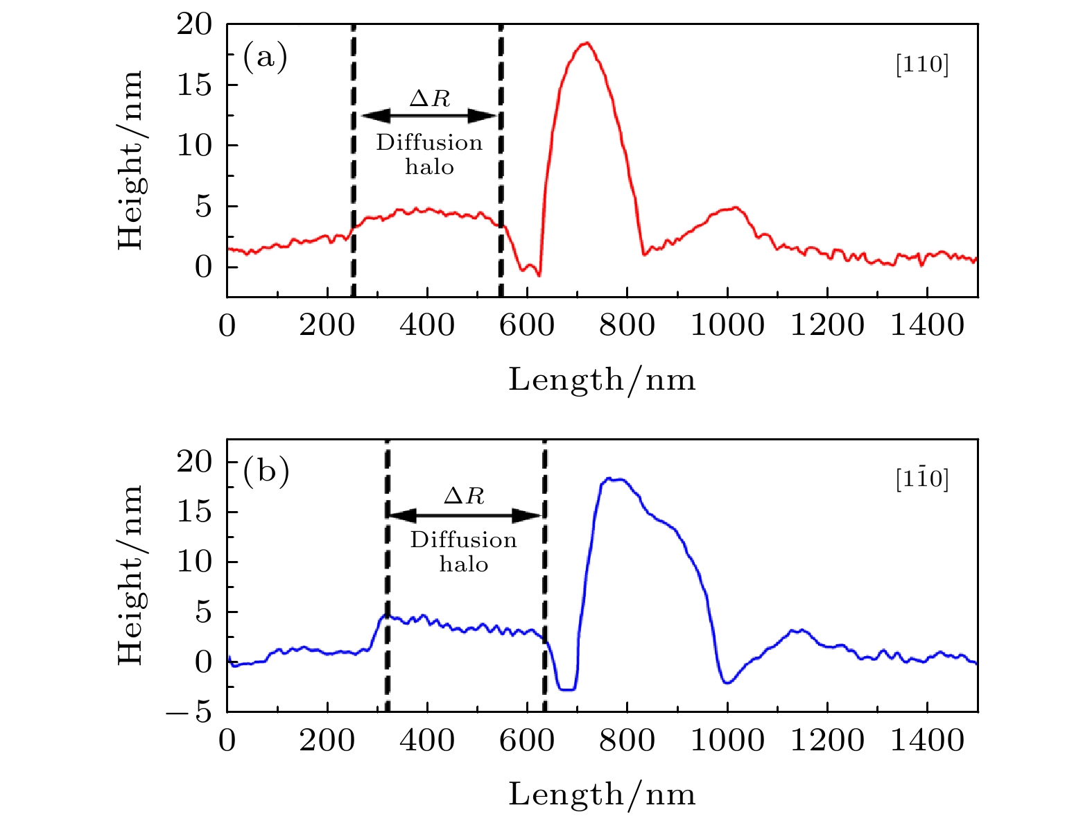
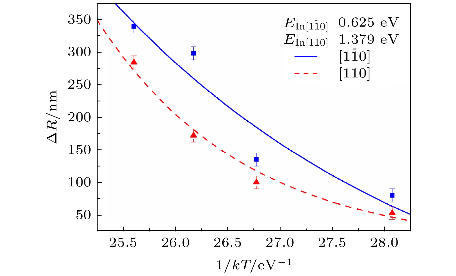
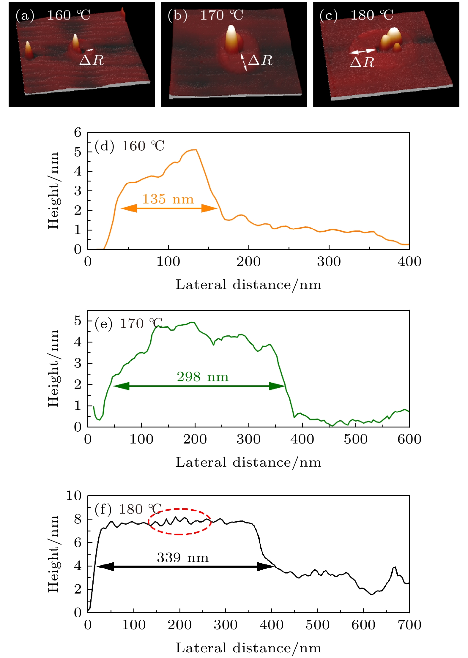
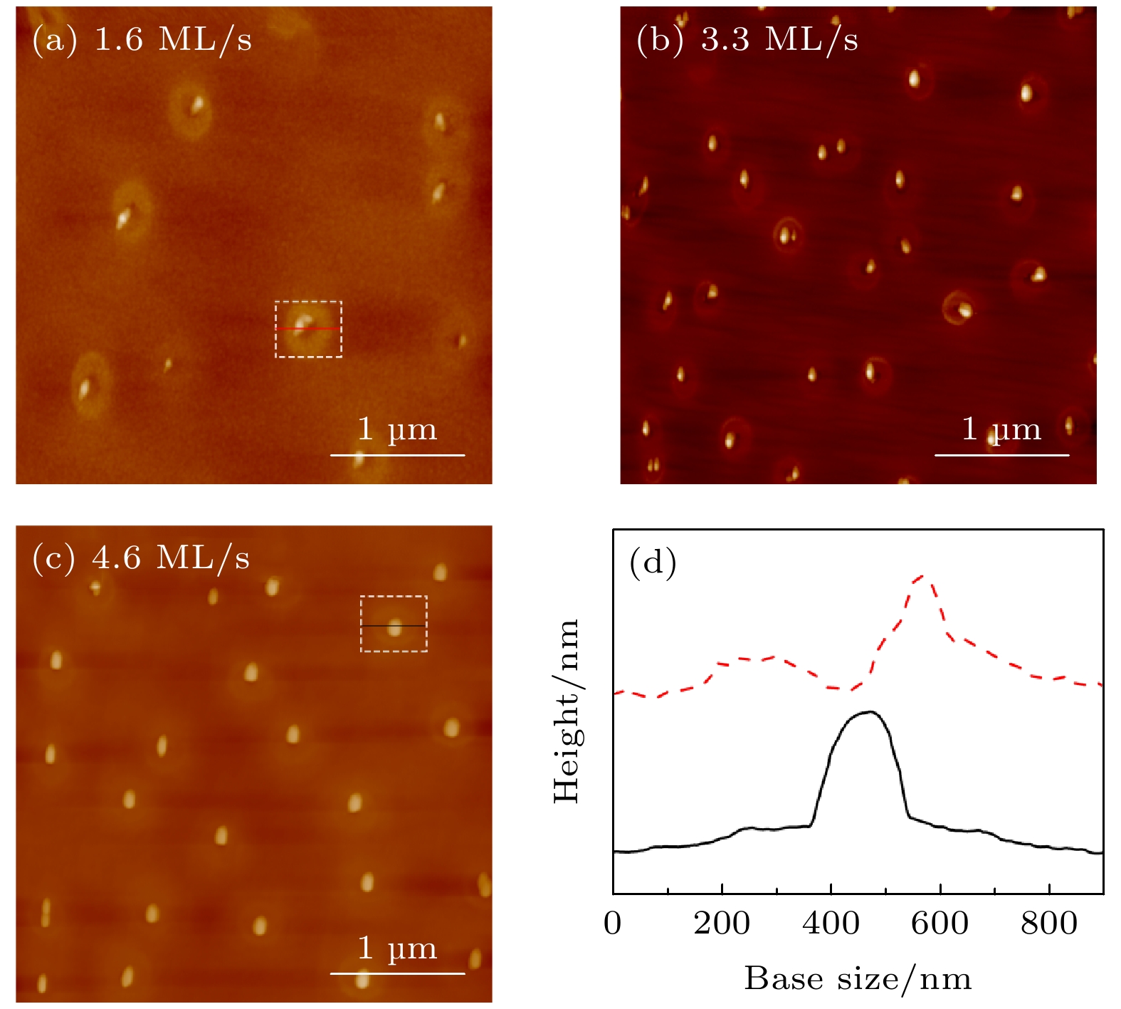
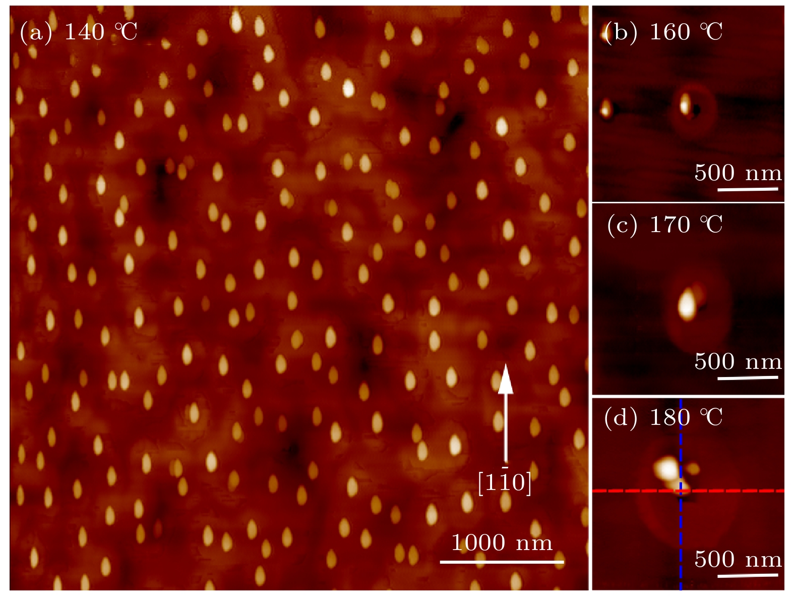
改变生长工艺、控制并调整液滴中原子扩散机制是对复杂纳米结构制备的关键途径, 并且对基于液滴外延方法研究半导体纳米结构十分重要. 本文在不同衬底温度, 不同As压下在GaAs(001)上沉积相同沉积量(5 monolayer)的In液滴并观察其表面形貌的变化. 原子力显微镜图像显示, 液滴晶化后所形成的扩散“盘”且呈现一定的对称性. 随着衬底温度的增高, 圆盘半径逐渐扩大, 扩散圆盘中心出现了坑. 而随着As压的增高, 所形成的液滴密度增加, 以液滴为中心所形成的扩散圆盘宽度逐渐减小. 基于经典的成核扩散理论对实验数据拟合得到: GaAs(001))表面In原子在
$ [1\bar10] $ 和[110]晶向上的扩散激活能分别为(0.62 ± 0.01) eV和(1.37 ± 0.01) eV, 且扩散系数D0为1.2 × 10⁻² cm2/s. 对比其他研究小组的结果证实了理论的正确性. 实验中得到的In原子的扩散激活能以及In液滴在GaAs(001)上扩散机理, 可以为InAs纳米结构特性的调制提供实验指导.In recent years, low-dimensional nanostructures such as quantum dots (QD) and quantum rings (QR) have been widely used in many fields such as optoelectronics, microelectronics and quantum communication due to their unique electrical, optical and magnetic properties. Owing to the similarity between nanostructures and atomic systems, the flexible modulation of several quantum properties of nanomaterials and the preparation of new optoelectronic devices around the characteristics of these structural systems have become a hot topic of research. Changing the growth process to control and tune the atomic diffusion mechanism in droplets is a key way of preparing complex nanostructures, which is important for the study of semiconductor nanostructure by droplet epitaxy. In the present experiment, the same amount (5 monolayer (5 ML)) of indium is deposited on GaAs (001) at different substrate temperatures (140, 160, 170 and 180 ℃) and different arsenic pressures (1.6, 3.3 and 4.6 ML/s), and the surface morphology evolutions are observed. As the substrate temperature increases, the radius of the disk gradually expands and a pit appears in the center of the diffusion disk. As the arsenic pressure increases, the density of the formed droplets increases, and the width of the diffusion disk formed in the center of the droplets gradually decreases. Our work involving nucleation theory is done at T < 200 ℃ to deactivate many thermal processes. This is a result of the diffusion coefficient being more complexly related to temperature. Based on the classical nucleation diffusion theory, the results of experimental data fitting include that the diffusion activation energies of In atoms on the surface of GaAs (001) are (0.62 ± 0.01) eV in$ [1\bar 10] $ and (1.37 ± 0.01) eV in [110] respectively, and that the diffusion coefficient D0 is 1.2 × 10⁻² cm2/s:those results confirm the theory after having been compared with the results obtained by other research groups. The diffusion activation energy of indium atoms and the diffusion mechanism of indium droplets on GaAs (001) obtained from the experiment can provide experimental guidance for modulating the structural property of InAs nanostructures.-
Keywords:
- InAs nanostructures /
- surface diffusion /
- droplet epitaxy
[1] Massimo G, Zhiming W, Armando R, Takashi K, Stefano S 2019 Nat. Mater. 5 799
[2] Francesco B B, Sergio B, Marcus R, Luca E, Alexey F, Daniel H, Armando R, Emiliano B, Rinaldo T, Stefano S 2018 Nano Lett. 18 505
 Google Scholar
[3] Zocher M, Heyn C, Hansen W 2019 J. Cryst. Growth 512 219
 Google Scholar
[4] Sergey V B, Maxim S S, Mikhail M E, Boris G K, Oleg A A 2019 Nanotechnology 30 505601
 Google Scholar
[5] Ying Y, Hancheng Z, Jiawei Y, Lin L, Jin L, Siyuan Y 2019 Nanotechnology 30 485001
 Google Scholar
[6] Jong S K, Im S H, Sang J L, Jin D S 2018 J. Korean Phys. Soc. 73 190
 Google Scholar
[7] Li A Z, Wang Z M, Wu J, Salamo G J 2010 Nano Res. 3 490
 Google Scholar
[8] Pankaow N, Thainoi S, Panyakeow S, Ratanathammaphan S 2011 J. Cryst. Growth. 323 282
 Google Scholar
[9] Boonpeng P, Jevasuwan W, Nuntawong N, Thainoi S, Panyakeow S, Ratanathammaphan S 2011 J. Cryst. Growth 323 271
 Google Scholar
[10] Boonpeng P, Kiravittaya S, Thainoi S, Panyakeow S, Ratanathammaphan S 2013 J. Cryst. Growth 378 435
 Google Scholar
[11] Pankaow N, Prongjit P, Thainoi S, Panyakeow S, Ratanathammaphan S 2013 Microelectron. Eng. 110 298
 Google Scholar
[12] Biccari F, Bietti S, Cavigli L, Vinattieri A, Nötzel R, Gurioli M 2016 J. Appl. Phys. 120 134312
 Google Scholar
[13] Nataliya L S, Maxim A V, Alla G N, Igor G N 2018 Comput. Mater. Sci. 141 91
 Google Scholar
[14] David F, Kamal A, Benito A, Yolanda G, Luisa G 2016 J. Cryst. Growth 434 81
 Google Scholar
[15] Noda T, Jo M, Mano T, Kawazu T, Sakaki H 2013 J. Cryst. Growth 378 529
 Google Scholar
[16] Jong S K 2017 Mater. Sci. Semicond. Process. 57 70
 Google Scholar
[17] Spirina A A, Shwartz N L 2019 Mater. Sci. Semicond. Process. 100 319
 Google Scholar
[18] Chawner J M A, Chang Y, Hodgson P D, Hayne M, Robson A J, Sanchez A M, Zhuang Q 2019 Semicond. Sci. Technol. 34 9
[19] Zhao C J 2018 J. Nanosci. Nanotechnol. 18 7617
 Google Scholar
[20] Bietti S, Somaschini C, Esposito L, Fedorov A, Sanguinetti S 2014 J. Appl. Phys. 116 114311
 Google Scholar
[21] Somaschini C, Bietti S, Koguchi N, Sanguinetti S 2010 Appl. Phys. Lett. 97 203109
 Google Scholar
[22] Takeshi N, Takaaki M, Hiroyuki S 2011 Cryst. Growth. Des. 11 726
 Google Scholar
[23] Rosini M, Righi M C, Kratzer P, Magri R 2009 Phys. Rev. B 79 075302
 Google Scholar
[24] Margaret A S, Stephanie T, Sergey M, Thomas EV, Michael KY 2017 J. Appl. Phys. 121 195302
 Google Scholar
-
表 1 本文得到的EIn值与文献的比较
Table 1. Comparison of the EIn values obtained in this paper with the literatures.
References Material system EIn/eV Method Takeshi等[24] InAs/GaAs [110]: 0.34
$ [1\bar 10] $: 0.21Droplet epitaxy Margaret等[23] InAs/InGaAs/InP [110]: 0.686 ± 0.04
$ [1\bar 10] $: 0.546 ± 0.03Droplet epitaxy Rosini等[22] InAs/InGaAs/GaAs [110]: 0.8–1.0
$ [1\bar 10] $: 0.4–0.9Simulation: KMC and DFT Our work InAs/GaAs [110]: 1.37 ± 0.01
$ [1\bar 10] $: 0.62 ± 0.01Droplet epitaxy -
[1] Massimo G, Zhiming W, Armando R, Takashi K, Stefano S 2019 Nat. Mater. 5 799
[2] Francesco B B, Sergio B, Marcus R, Luca E, Alexey F, Daniel H, Armando R, Emiliano B, Rinaldo T, Stefano S 2018 Nano Lett. 18 505
 Google Scholar
[3] Zocher M, Heyn C, Hansen W 2019 J. Cryst. Growth 512 219
 Google Scholar
[4] Sergey V B, Maxim S S, Mikhail M E, Boris G K, Oleg A A 2019 Nanotechnology 30 505601
 Google Scholar
[5] Ying Y, Hancheng Z, Jiawei Y, Lin L, Jin L, Siyuan Y 2019 Nanotechnology 30 485001
 Google Scholar
[6] Jong S K, Im S H, Sang J L, Jin D S 2018 J. Korean Phys. Soc. 73 190
 Google Scholar
[7] Li A Z, Wang Z M, Wu J, Salamo G J 2010 Nano Res. 3 490
 Google Scholar
[8] Pankaow N, Thainoi S, Panyakeow S, Ratanathammaphan S 2011 J. Cryst. Growth. 323 282
 Google Scholar
[9] Boonpeng P, Jevasuwan W, Nuntawong N, Thainoi S, Panyakeow S, Ratanathammaphan S 2011 J. Cryst. Growth 323 271
 Google Scholar
[10] Boonpeng P, Kiravittaya S, Thainoi S, Panyakeow S, Ratanathammaphan S 2013 J. Cryst. Growth 378 435
 Google Scholar
[11] Pankaow N, Prongjit P, Thainoi S, Panyakeow S, Ratanathammaphan S 2013 Microelectron. Eng. 110 298
 Google Scholar
[12] Biccari F, Bietti S, Cavigli L, Vinattieri A, Nötzel R, Gurioli M 2016 J. Appl. Phys. 120 134312
 Google Scholar
[13] Nataliya L S, Maxim A V, Alla G N, Igor G N 2018 Comput. Mater. Sci. 141 91
 Google Scholar
[14] David F, Kamal A, Benito A, Yolanda G, Luisa G 2016 J. Cryst. Growth 434 81
 Google Scholar
[15] Noda T, Jo M, Mano T, Kawazu T, Sakaki H 2013 J. Cryst. Growth 378 529
 Google Scholar
[16] Jong S K 2017 Mater. Sci. Semicond. Process. 57 70
 Google Scholar
[17] Spirina A A, Shwartz N L 2019 Mater. Sci. Semicond. Process. 100 319
 Google Scholar
[18] Chawner J M A, Chang Y, Hodgson P D, Hayne M, Robson A J, Sanchez A M, Zhuang Q 2019 Semicond. Sci. Technol. 34 9
[19] Zhao C J 2018 J. Nanosci. Nanotechnol. 18 7617
 Google Scholar
[20] Bietti S, Somaschini C, Esposito L, Fedorov A, Sanguinetti S 2014 J. Appl. Phys. 116 114311
 Google Scholar
[21] Somaschini C, Bietti S, Koguchi N, Sanguinetti S 2010 Appl. Phys. Lett. 97 203109
 Google Scholar
[22] Takeshi N, Takaaki M, Hiroyuki S 2011 Cryst. Growth. Des. 11 726
 Google Scholar
[23] Rosini M, Righi M C, Kratzer P, Magri R 2009 Phys. Rev. B 79 075302
 Google Scholar
[24] Margaret A S, Stephanie T, Sergey M, Thomas EV, Michael KY 2017 J. Appl. Phys. 121 195302
 Google Scholar
计量
- 文章访问数: 2644
- PDF下载量: 49
- 被引次数: 0


 下载:
下载:
