


-
With the development of the semiconductor manufacturing process, the size of the metal-oxide-semiconductor field-effect transistor (MOSFET) device has been on a tens-of-nanometer scale. The shot noise appears in the excess channel noise of the device, and the noise mechanism of the device begins to change gradually. Due to the fact that the electron temperature gradient is neglected in calculation and the significant enhancement of the lateral channel electric field are not taken into consideration, the traditional electron temperature model and the thermal noise model underestimate the effect of hot carrier effects, resulting in the underestimate of the thermal noise. Moreover, the traditional drain-source current model ignores the electron temperature gradient in the calculation and does not include the effect of the electron temperature on the mobility degradation effect either. Therefore, the calculation accuracy of the shot noise and the Fano factor on the basis of the traditional model will be reduced to a certain extent as the size of the device decreases, thus affecting the analysis of the noise mechanism of the device. In this paper, we establish the channel electron temperature model and the electron velocity model by solving the energy balance equation, and develop the drain source current model based on these two models. Moreover, the shot noise model and the thermal noise model suitable for devices below 40 nm are established based on the drain-source current model. Meanwhile, the Fano factor of the shot noise is calculated. The influence of the MOSFET device size on the noise mechanism and the Fano factor of the shot noise are also investigated when the device is under different bias voltages. The results show that the accuracy of the existing thermal noise model and the shot noise model decline as the device size decreases, which eventually leads the Fano factor of the shot noise to be overestimated. When the size of the NMOSFET device is below 20 nm, the shot noise affects the device noise in the strong inversion region. With the size decreasing, the characteristic of the noise mechanism of the NMOSFET device changes from the characteristic of single thermal noise to the common characteristic of both the thermal noise and the shot noise. When the NMOSFET device size is scaled down to 10 nm, the channel noise of the device can no longer be characterized by the thermal noise alone. Instead, the noise mechanism of the device changes and is characterized by both the channel thermal noise and the suppressed shot noise. The shot noise has become an important factor that contributes to the excessive noise in the device. -
Keywords:
- shot noise /
- Fano factor /
- electron temperature /
- short channel /
- field effect transistor
[1] Scholten A J, Tiemeijer L F, Duijnhoven A T A Z, Havens R J, Kort R, Langevelde R, Klaassen D B M, Jeamsaksiri W, Velghe R M D A 2005 International Conference on Noise and Fluctuations Salamanca, Spain, September 19−23, 2005 p735
[2] 贾晓菲, 杜磊, 唐冬和, 王婷岚, 陈文豪 2012 物理学报 61 127202
 Google Scholar
Jia X F, Du L, Tang D H, Wang T L, Chen W H 2012 Acta Phys. Sin. 61 127202
Google Scholar
[3] Do V A, Dollfus P, Nguyen V L 2007 J. Comput. Electron. 6 125
Google Scholar
[4] Spathis C, Georgakopoulou K, Birbas A 2013 22nd International Conference on Noise and Fluctuations (ICNF) Montpellier, France, June 24−28, 2013 p1
[5] Navid R 2007 J. Appl. Phys. 101 124501
Google Scholar
[6] Jia X F, He L 2017 AIP Adv. 7 055202
Google Scholar
[7] Teng H F, Jang S L, Juang M H 2003 Solid-State Electron. 47 2043
Google Scholar
[8] Chan L H K, Yeo K S, Chew K W J, Ong S N, Loo X S, Boon C C, Do M A 2012 IEEE Electron Device Lett. 33 1117
Google Scholar
[9] 唐冬和, 杜磊, 王婷岚, 陈华, 贾晓菲 2011 物理学报 60 097202
Google Scholar
Tang D H, Du L, Wang T L, Chen H, Jia X F 2011 Acta Phys. Sin. 60 097202
Google Scholar
[10] Jeon J, Kang M 2016 Jpn. J. Appl. Phys. 55 054102
Google Scholar
[11] Jeon J, Lee J, Kim J, Park C H, Lee H, Oh H, Kang H K, Park B G, Shin H 2009 Symposium on VLSI Technology Honolulu, HI, USA, June 15−17, 2009 p48
[12] Smit G D J, Scholten A J, Pijper R M T, Tiemeijer L F, Toorn R V D, Klaassen D B M 2014 IEEE Trans. Electron Devices 61 245
Google Scholar
[13] 王军, 王林, 王丹丹 2016 物理学报 65 237102
Google Scholar
Wang J, Wang L, Wang D D 2016 Acta Phys. Sin. 65 237102
Google Scholar
[14] Wang J, Peng X M, Liu Z J, Wang L, Luo Z, Wang D D 2018 Chin. Phys. B 27 027201
Google Scholar
[15] Mahajan V M, Patalay P R, Jindal R P, Shichijo H, Martin S, Hou F C, Machala C, Trombley D E 2012 IEEE Trans. Electron Devices 59 197
Google Scholar
[16] Chen X S, Chen C H, Deen M J 2017 International Conference on Noise and Fluctuations (ICNF) Vilnius, Lithuania, June 20−13, 2017 p1
[17] Spathis C, Birbas A, Georgakopoulou K 2015 AIP Adv. 5 087114
Google Scholar
[18] Wang J 2017 Electron. Lett. 53 1671
Google Scholar
[19] Barral V, Poiroux T, Saint-Martin J, Munteanu D, Autran J L, Deleonibus S 2009 IEEE Trans. Electron Devices 56 408
Google Scholar
[20] Shen Y F, Cui J, Mohammadi S 2017 Solid-State Electron. 131 45
Google Scholar
[21] Chen X S, Chih H C, Ryan L 2018 IEEE Trans. Electron Devices 65 1502
Google Scholar
[22] Lu Z Q, Lai F C 2009 Analog. Integr. Circ. Process 59 185
Google Scholar
[23] Lee K Y 2017 Solid-State Electron. 130 63
Google Scholar
[24] Chen C H, Deen M J 2002 IEEE Trans. Electron Devices 49 1484
Google Scholar
[25] 艾罗拉 N 著 (张兴, 李映雪 译) 1999 用于VLSI模拟的小尺寸MOS器件模型 (北京: 科学出版社) 第248−251页
Arora N (translated by Zhang X, Li Y X) 1999 MOSFET Models for VLSI Circuit Simulation (Beijing: Science Press) pp248−251 (in Chinese)
[26] Lim K Y, Zhou X 2002 Microelectron. Reliab. 42 1857
Google Scholar
[27] Wei C Q, See G H, Zhou X, Chan L 2008 IEEE Trans. Electron Devices 55 2378
Google Scholar
[28] Ong S N, Yeo K S, Chew K W J, Chan L H K, Loo X S, Boon C C, Do M A 2012 Solid-State Electron. 68 32
Google Scholar
[29] Lundstrom M 2009 Fundamentals of Carrier Transport (2nd Ed.) (Cambridge: Cambridge University Press) pp230−293
[30] Tsividis Y 2011 Operation and Modeling of the MOS Transistor (3rd Ed.) (New York: Oxford University Press) pp194−201
[31] Ong S N, Yeo K S, Chew K W J, Chan L H K, Loo X S, Boon C C, Do M A 2012 Solid-State Electron. 72 8
Google Scholar
[32] Paasschens J C J, Scholten A J, van Langevelde R 2005 IEEE Trans. Electron Devices 52 2463
Google Scholar
[33] Li Z Y, Ma J G, Ye Y Z, Yu M Y 2009 IEEE Trans. Electron Devices 56 1300
Google Scholar
[34] 张梦, 姚若河, 刘玉荣 2020 物理学报 69 057101
Google Scholar
Zhang M, Yao R H, Liu Y R 2020 Acta Phys. Sin. 69 057101
Google Scholar
[35] Chen C H, Chen D, Lee R, Lei P, Wan D 2013 Proceedings of the IEEE 2013 Custom Integrated Circuits Conference San Jose, CA, USA, September 22−25, 2013 p1
[36] Yamaguchi K, Sakurai S, Tomizawa K 2010 Jpn. J. Appl. Phys. 49 024303
Google Scholar
-
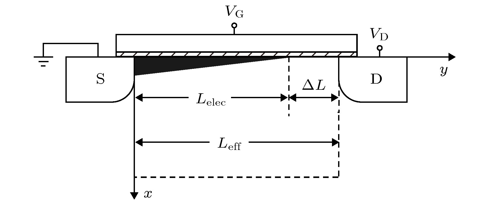
图 1 NMOSFET器件的结构示意图
Figure 1. Structure diagram of the NMOSFET device.
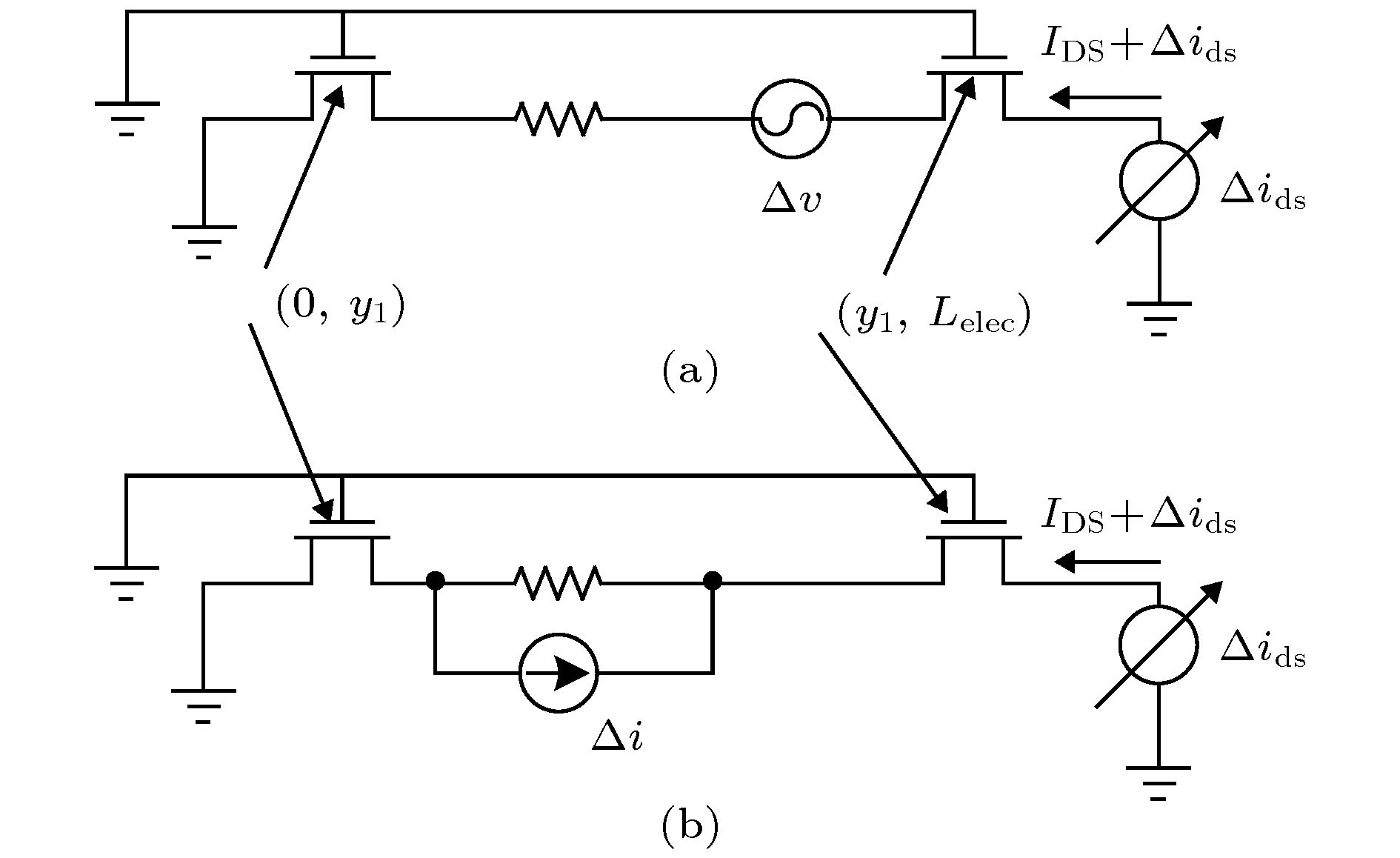
图 2 沟道中含虚拟直流源的晶体管结构图
Figure 2. Schematic diagram of the transistor with a fictitious dc source in the channel.

图 3 全散粒噪声和热噪声随栅源偏置电压的变化(Leff = 40 nm)
Figure 3. Full-shot noise and thermal noise vs. gate-source bias voltage (Leff = 40 nm).

图 4 散粒噪声抑制因子随栅源偏置电压的变化(Leff = 40 nm)
Figure 4. Fano factor of shot noise vs. gate-source bias voltage (Leff = 40 nm).
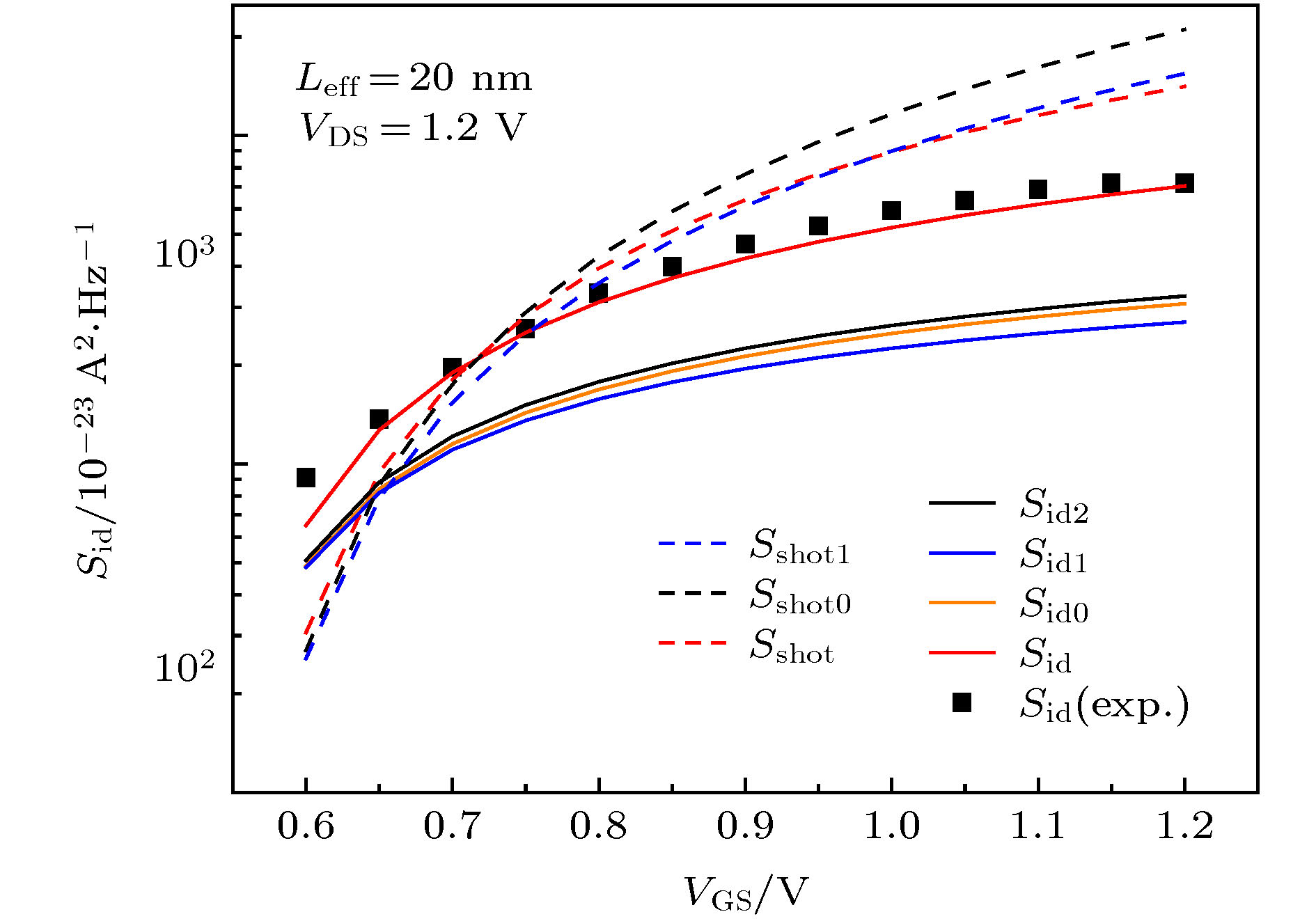
图 5 全散粒噪声和热噪声随栅源偏置电压的变化(Leff = 20 nm)
Figure 5. Full-shot noise and thermal noise vs. gate-source bias voltage (Leff = 20 nm).
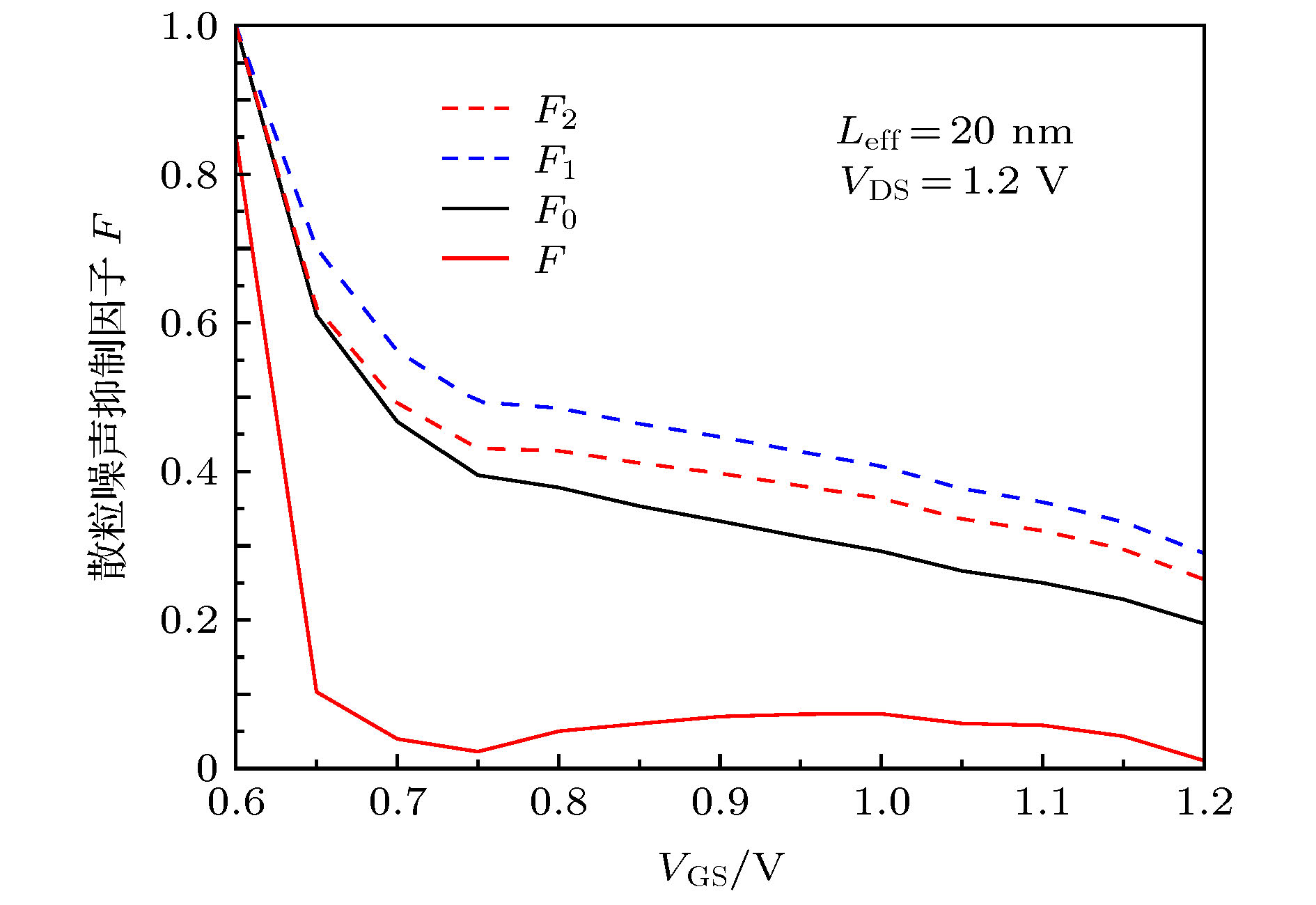
图 6 散粒噪声抑制因子随栅源偏置电压的变化(Leff = 20 nm)
Figure 6. Fano factor of shot noise vs. gate-source bias voltage (Leff = 20 nm).
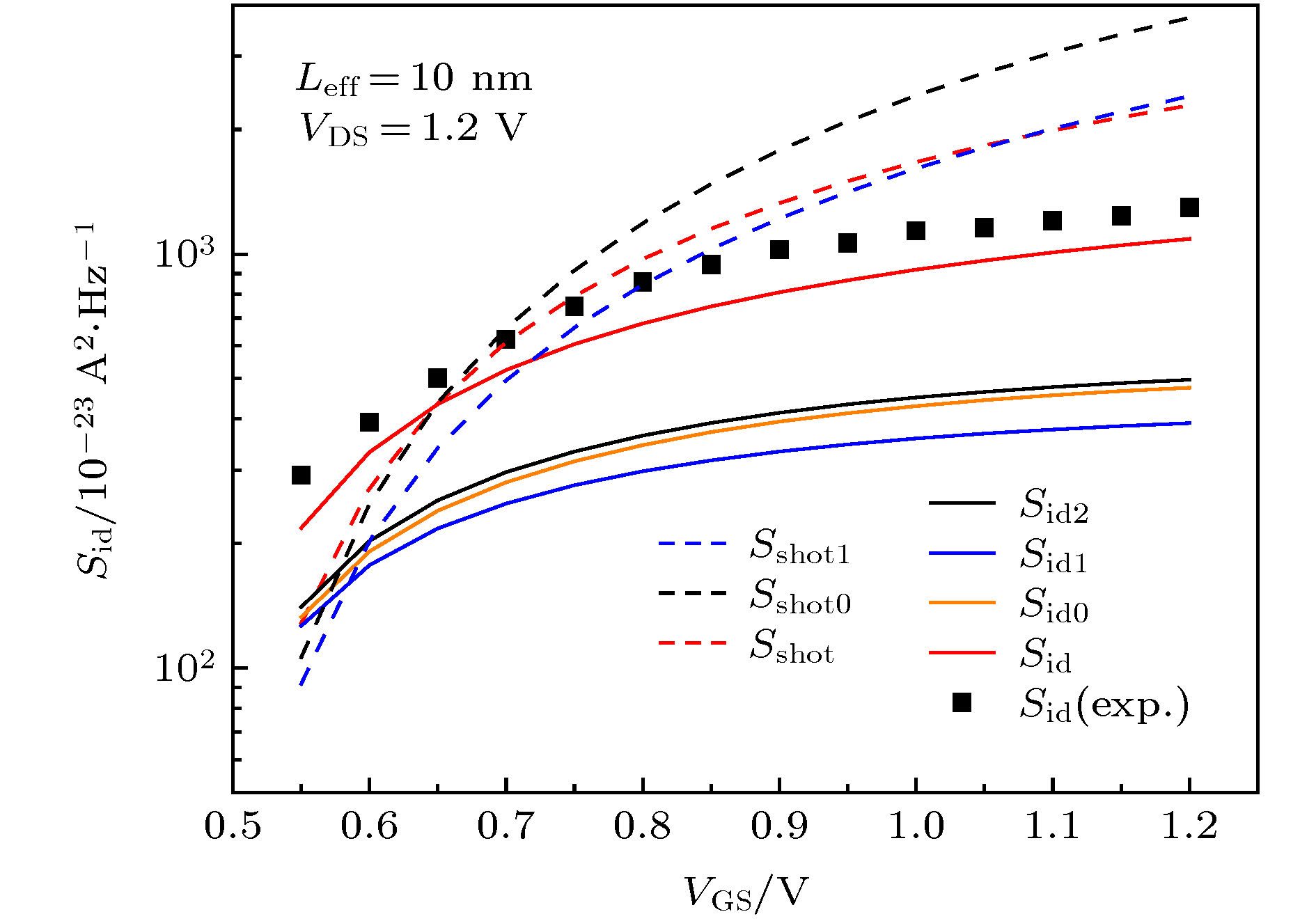
图 7 全散粒噪声和热噪声随栅源偏置电压的变化(Leff = 10 nm)
Figure 7. Full-shot noise and thermal noise vs. gate-source bias voltage (Leff = 10 nm).
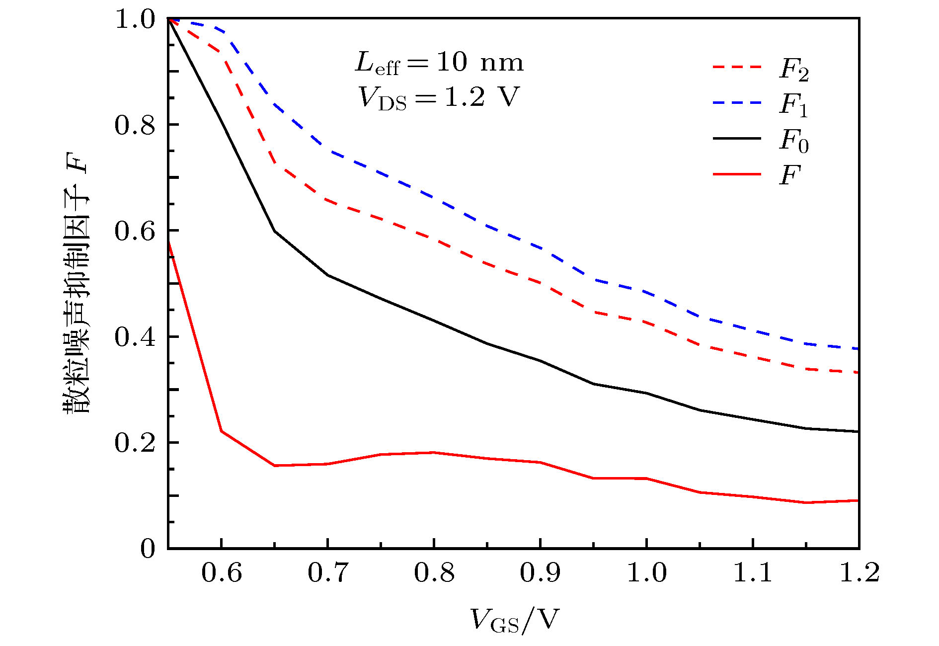
图 8 散粒噪声抑制因子随栅源偏置电压的变化(Leff = 10 nm)
Figure 8. Fano factor of shot noise vs. gate-source bias voltage (Leff = 10 nm).
-
[1] Scholten A J, Tiemeijer L F, Duijnhoven A T A Z, Havens R J, Kort R, Langevelde R, Klaassen D B M, Jeamsaksiri W, Velghe R M D A 2005 International Conference on Noise and Fluctuations Salamanca, Spain, September 19−23, 2005 p735
[2] 贾晓菲, 杜磊, 唐冬和, 王婷岚, 陈文豪 2012 物理学报 61 127202
Google Scholar
Jia X F, Du L, Tang D H, Wang T L, Chen W H 2012 Acta Phys. Sin. 61 127202
Google Scholar
[3] Do V A, Dollfus P, Nguyen V L 2007 J. Comput. Electron. 6 125
Google Scholar
[4] Spathis C, Georgakopoulou K, Birbas A 2013 22nd International Conference on Noise and Fluctuations (ICNF) Montpellier, France, June 24−28, 2013 p1
[5] Navid R 2007 J. Appl. Phys. 101 124501
Google Scholar
[6] Jia X F, He L 2017 AIP Adv. 7 055202
Google Scholar
[7] Teng H F, Jang S L, Juang M H 2003 Solid-State Electron. 47 2043
Google Scholar
[8] Chan L H K, Yeo K S, Chew K W J, Ong S N, Loo X S, Boon C C, Do M A 2012 IEEE Electron Device Lett. 33 1117
Google Scholar
[9] 唐冬和, 杜磊, 王婷岚, 陈华, 贾晓菲 2011 物理学报 60 097202
Google Scholar
Tang D H, Du L, Wang T L, Chen H, Jia X F 2011 Acta Phys. Sin. 60 097202
Google Scholar
[10] Jeon J, Kang M 2016 Jpn. J. Appl. Phys. 55 054102
Google Scholar
[11] Jeon J, Lee J, Kim J, Park C H, Lee H, Oh H, Kang H K, Park B G, Shin H 2009 Symposium on VLSI Technology Honolulu, HI, USA, June 15−17, 2009 p48
[12] Smit G D J, Scholten A J, Pijper R M T, Tiemeijer L F, Toorn R V D, Klaassen D B M 2014 IEEE Trans. Electron Devices 61 245
Google Scholar
[13] 王军, 王林, 王丹丹 2016 物理学报 65 237102
Google Scholar
Wang J, Wang L, Wang D D 2016 Acta Phys. Sin. 65 237102
Google Scholar
[14] Wang J, Peng X M, Liu Z J, Wang L, Luo Z, Wang D D 2018 Chin. Phys. B 27 027201
Google Scholar
[15] Mahajan V M, Patalay P R, Jindal R P, Shichijo H, Martin S, Hou F C, Machala C, Trombley D E 2012 IEEE Trans. Electron Devices 59 197
Google Scholar
[16] Chen X S, Chen C H, Deen M J 2017 International Conference on Noise and Fluctuations (ICNF) Vilnius, Lithuania, June 20−13, 2017 p1
[17] Spathis C, Birbas A, Georgakopoulou K 2015 AIP Adv. 5 087114
Google Scholar
[18] Wang J 2017 Electron. Lett. 53 1671
Google Scholar
[19] Barral V, Poiroux T, Saint-Martin J, Munteanu D, Autran J L, Deleonibus S 2009 IEEE Trans. Electron Devices 56 408
Google Scholar
[20] Shen Y F, Cui J, Mohammadi S 2017 Solid-State Electron. 131 45
Google Scholar
[21] Chen X S, Chih H C, Ryan L 2018 IEEE Trans. Electron Devices 65 1502
Google Scholar
[22] Lu Z Q, Lai F C 2009 Analog. Integr. Circ. Process 59 185
Google Scholar
[23] Lee K Y 2017 Solid-State Electron. 130 63
Google Scholar
[24] Chen C H, Deen M J 2002 IEEE Trans. Electron Devices 49 1484
Google Scholar
[25] 艾罗拉 N 著 (张兴, 李映雪 译) 1999 用于VLSI模拟的小尺寸MOS器件模型 (北京: 科学出版社) 第248−251页
Arora N (translated by Zhang X, Li Y X) 1999 MOSFET Models for VLSI Circuit Simulation (Beijing: Science Press) pp248−251 (in Chinese)
[26] Lim K Y, Zhou X 2002 Microelectron. Reliab. 42 1857
Google Scholar
[27] Wei C Q, See G H, Zhou X, Chan L 2008 IEEE Trans. Electron Devices 55 2378
Google Scholar
[28] Ong S N, Yeo K S, Chew K W J, Chan L H K, Loo X S, Boon C C, Do M A 2012 Solid-State Electron. 68 32
Google Scholar
[29] Lundstrom M 2009 Fundamentals of Carrier Transport (2nd Ed.) (Cambridge: Cambridge University Press) pp230−293
[30] Tsividis Y 2011 Operation and Modeling of the MOS Transistor (3rd Ed.) (New York: Oxford University Press) pp194−201
[31] Ong S N, Yeo K S, Chew K W J, Chan L H K, Loo X S, Boon C C, Do M A 2012 Solid-State Electron. 72 8
Google Scholar
[32] Paasschens J C J, Scholten A J, van Langevelde R 2005 IEEE Trans. Electron Devices 52 2463
Google Scholar
[33] Li Z Y, Ma J G, Ye Y Z, Yu M Y 2009 IEEE Trans. Electron Devices 56 1300
Google Scholar
[34] 张梦, 姚若河, 刘玉荣 2020 物理学报 69 057101
Google Scholar
Zhang M, Yao R H, Liu Y R 2020 Acta Phys. Sin. 69 057101
Google Scholar
[35] Chen C H, Chen D, Lee R, Lei P, Wan D 2013 Proceedings of the IEEE 2013 Custom Integrated Circuits Conference San Jose, CA, USA, September 22−25, 2013 p1
[36] Yamaguchi K, Sakurai S, Tomizawa K 2010 Jpn. J. Appl. Phys. 49 024303
Google Scholar

 DownLoad:
Catalog
Metrics
- Abstract views: 6733
- PDF Downloads: 101
- Cited By: 0
