


-
Shield-gate trench MOSFET in a low-to-medium voltage range (12-250 V) plays a key role in the power conversion market due to its low power loss caused by the sheild-gate structure. In order to eliminate the faults resulting from the parasitic effects of the device and improve the conversion efficiency, the device model is indispensable in designing a circuit system. In this paper, a compact model of shield-gate trench MOSFET based on BSIM4 is proposed, including the DC model and the capacitance model. In the DC model, the basic MOSFET structure uses BSIM4, and the equivalent resistances of the basic MOSFET in series are divided into three parts. The equivalent resistance model of JFET region is established by using the electric potential difference between both ends for the first time, and the equivalent resistance model of electron diffusion region is also introduced, in order to solve the problem of current error caused by neglecting the source potential of JFET region. The equivalent resistance between drain and JFET region and the equivalent resistance of electron diffusion region both prove to be constant. In the capacitance model based on BSIM4, the model of shield-gate to drain capacitance is added to the model of drain to source capacitance, and the voltage bias between drain and gate in the model of gate to drain capacitance is modified into the potential difference between the node at the end of the gate-drift overlap region and the gate. Poisson equations are used to solve the electric potential of this node. Furthermore, the gate oxide thickness factor k1, the shield-gate oxide thickness factor k2, the equivalent length of gate-drift overlap Lovequ and the equivalent length of shield-gate LSHequ are introduced to redefine the position of gate and shield-gate, thereby simplifying the Poisson equations and ensuring the smoothness of the potential curve of the node. Comparison of the data from the simulation by using Verilog-A program with the test results from the experimental platform shows that the model simulation results fit well with the test data, Therefore, the proposed model is verified.
-
Keywords:
- shield-gate trench MOSFET /
- compact model /
- BSIM4 /
- Verilog-A
[1] Wang Y, Hu H F, Yu C H, Wei J T 2015 IET Power Electronics 8 678
 Google Scholar
[2] Sarkar T, Sapp S, Challa A 2013 28th Annual IEEE Applied Power Electronics Conference and Exposition (APEC) Long Beach, USA, March 17−21, 2013 p507
[3] Park C, Havanur S, Shibib A, Terrill K 2016 28th International Symposium on Power Semiconductor Devices and ICs (ISPSD) Prague, Czech Republic, June 12–16, 2016 p387
[4] Tong C F, Cortes I, Mawby P A, Covington J A, Morancho F 2009 IEEE Spanish Conference on Electron Devices Santiago de Compostela Santiago de Compostela, Spain, February 11–13, 2009 p250
[5] Choi W, Son D, Young S 2012 27th Annual IEEE Applied Power Electronics Conference and Exposition (APEC) Orlando, USA, February 5–9, 2012 p1676
[6] Wang Y, Yu C H, Li M S, Cao F, Liu Y J 2017 IEEE Trans. Electron Devices 64 1455
Google Scholar
[7] Bao J, Qi H, Zhang J, Zhang Y, Hao Z 2011 6th IEEE Joint International Information Technology and Artificial Intelligence Conference Chongqing, China, August 20–22, 2011 p245
[8] 王磊, 杨华岳 2010 物理学报 59 0571
Google Scholar
Wang L, Yang Y H 2010 Acta Phys. Sin. 59 0571
Google Scholar
[9] Shi L, Jia K, Sun W 2013 IEEE Trans. Electron Devices 60 346
Google Scholar
[10] Tanaka A, Oritsuki Y, Kikuchihara H, Miyake M 2011 IEEE Trans. Electron Devices 58 2072
Google Scholar
[11] Victory J, Pearson S, Benczkowski S, Sarkar T, Jang H, Yazdi M B, Mao K 2016 28th International Symposium on Power Semiconductor Devices and ICs Prague, Czech Republic, June 12–16, 2016 p219
[12] Xiao Y, Victory J, Pearson S, Sarkar T, Challa A, Dagan M, Collanton P, Andreev C 2019 34th Annual IEEE Applied Power Electronics Conference and Exposition Anaheim, USA, March 17–21, 2019 p508
[13] Xi X, Dunga M, He J, Liu W, Cao K M, Jin X, Ou J J, Chan M, Niknejad A M http://cmosedu.com/cmos1/BSIM4_manual. pdf[2020-1-28]
[14] 巴利伽 B J 著 (韩郑生, 陆江, 宋李梅译) 2013 功率半导体器件基础 (北京: 电子工业出版社) 第197—198页
Baliga B J (translated by Han Z S, Lu J, Song L M) 2013 Fundamentals of Power Semiconductor Devices (Beijing: Publishing House of Electronics Industry) pp197–198 (in Chinese)
[15] Klein P 1997 IEEE Trans. Electron Devices 44 1483
Google Scholar
[16] Daniel B J, Parikh C D, Patil M B 2002 IEEE Trans. Electron Devices 49 916
Google Scholar
[17] Arribas A P, Shang F, Krishnamurthy M, Shenai K 2015 IEEE Trans. Electron Devices 62 1449
Google Scholar
[18] Ren M, Chen Z, Niu B, Cao X, Li S, Li Z, Zhang B 2016 IEEE International Nanoelectronics Conference (INEC) Chengdu, China, May 9–11, 2016 p1
[19] Chauhan Y S, Gillon R, Declercq M, Ionescu A M 2007 37th European Solid State Device Research Conference Munich, Germany, September 11–13, 2007 p426
[20] Shenai K 1991 IEEE Trans. Power Electron 6 539
Google Scholar
[21] Agarwal H, Gupta C, Goel R, Kushwaha P, Lin Y K, Kao M Y, Duarte J P, Chang H L, Chauhan Y S, Salahuddin S, Hu C 2019 IEEE Trans. Electron Devices 66 4258
Google Scholar
[22] Zhang W T, Ye L, Fang D, Qiao M, Xiao K, He B, Li Z, Zhang B 2019 IEEE Trans. Electron Devices 66 1416
Google Scholar
-
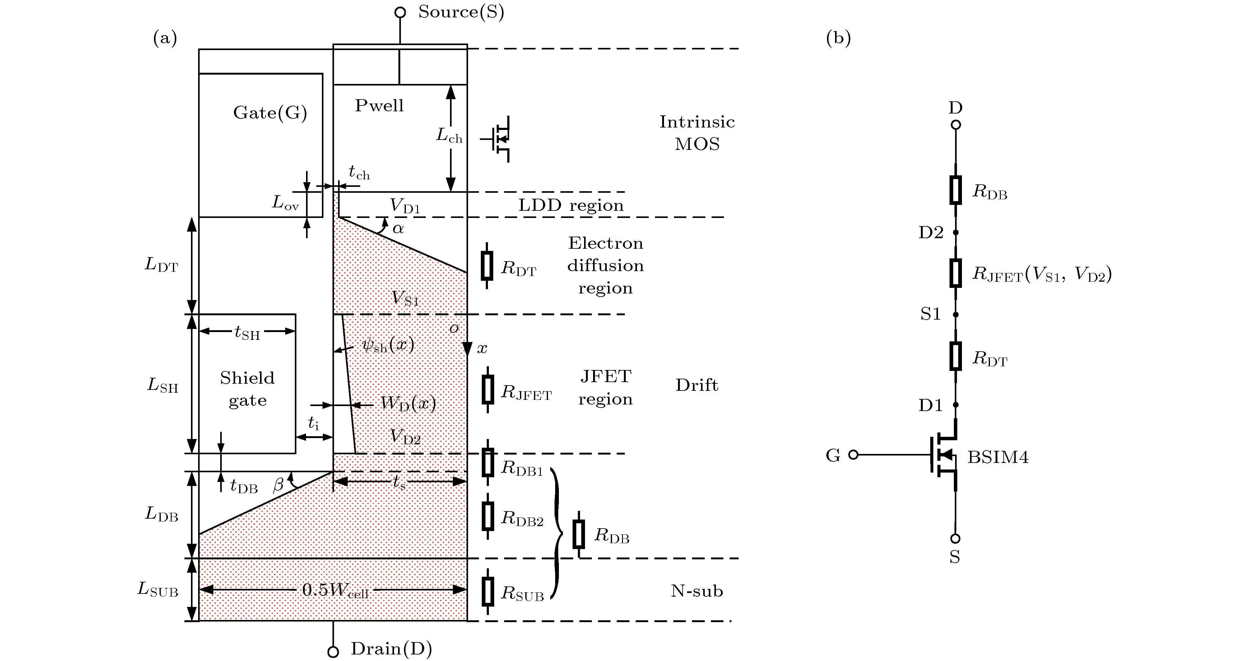
图 1 SGT MOS的等效电阻分布(a)和直流等效电路(b)
Figure 1. (a) Distribution of equivalent resistance of SGT MOS; (b) equivalent DC circuit of SGT MOS.
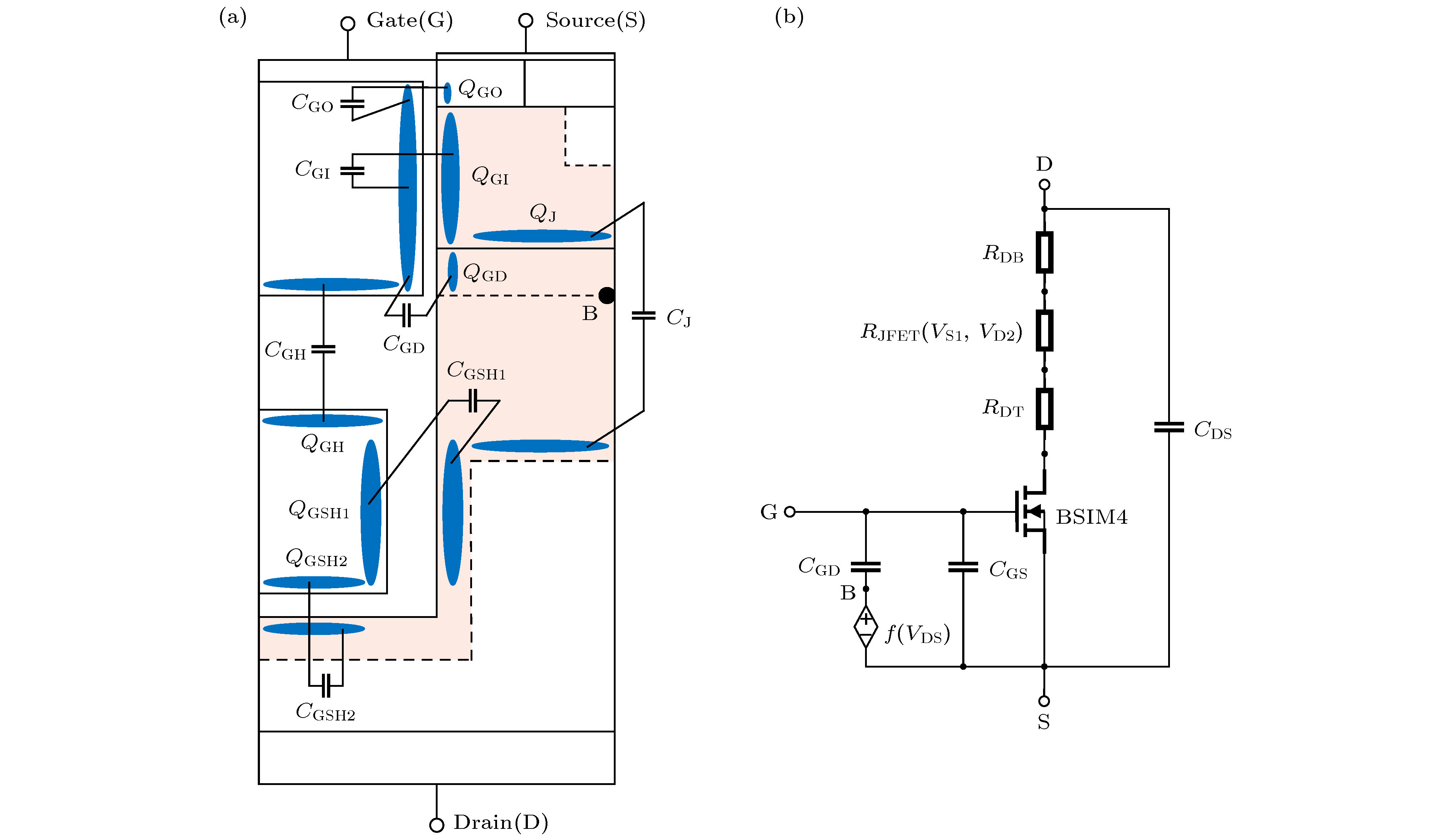
图 2 SGT MOS的电容和电荷的分布(a)及电容等效电路(b)
Figure 2. (a) Distribution of capacitance and charge of SGT MOS; (b) equivalent capacitance circuit of SGT MOS.

图 3 SGT MOS栅和屏蔽栅 (a) 等效前的结构示意图和 (b) 等效后的结构示意图
Figure 3. Schematic diagrams of structure before equivalence (a) and after equivalence (b).
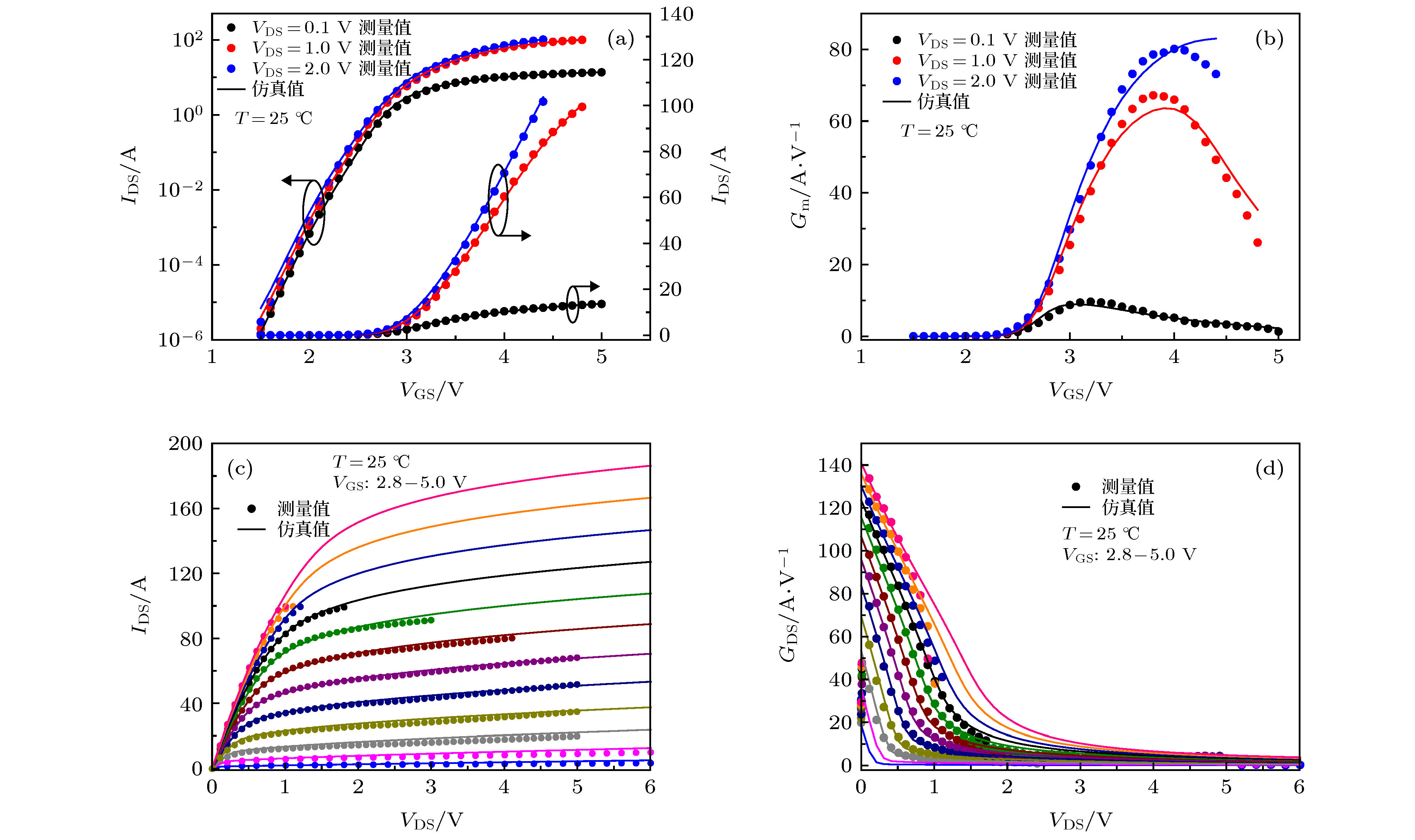
图 4 25 ℃下的 (a) 转移特性曲线, (b) 跨导Gm曲线, (c) 输出特性曲线和 (d) 输出电导GDS曲线
Figure 4. The curves of (a) transfer characteristic, (b) transconductance Gm, (c) output characteristic and (d) output conductance GDS at 25 ℃.
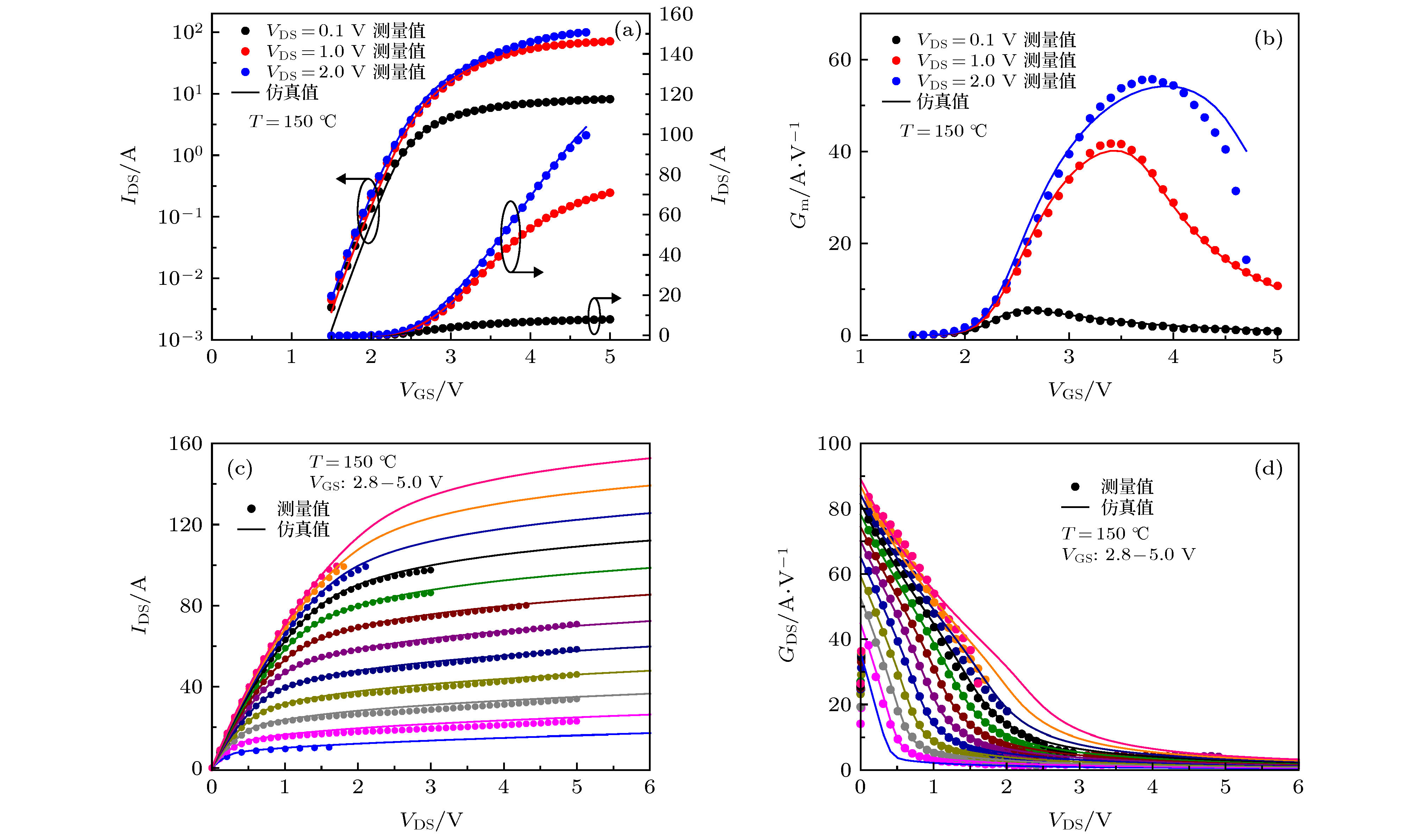
图 5 150 ℃下的 (a) 转移特性曲线, (b) 跨导Gm曲线, (c) 输出特性曲线和 (d) 输出电导GDS曲线
Figure 5. The curves of (a) transfer characteristic, (b) transconductance Gm, (c) output characteristic and (d) output conductance GDS at 150 ℃.
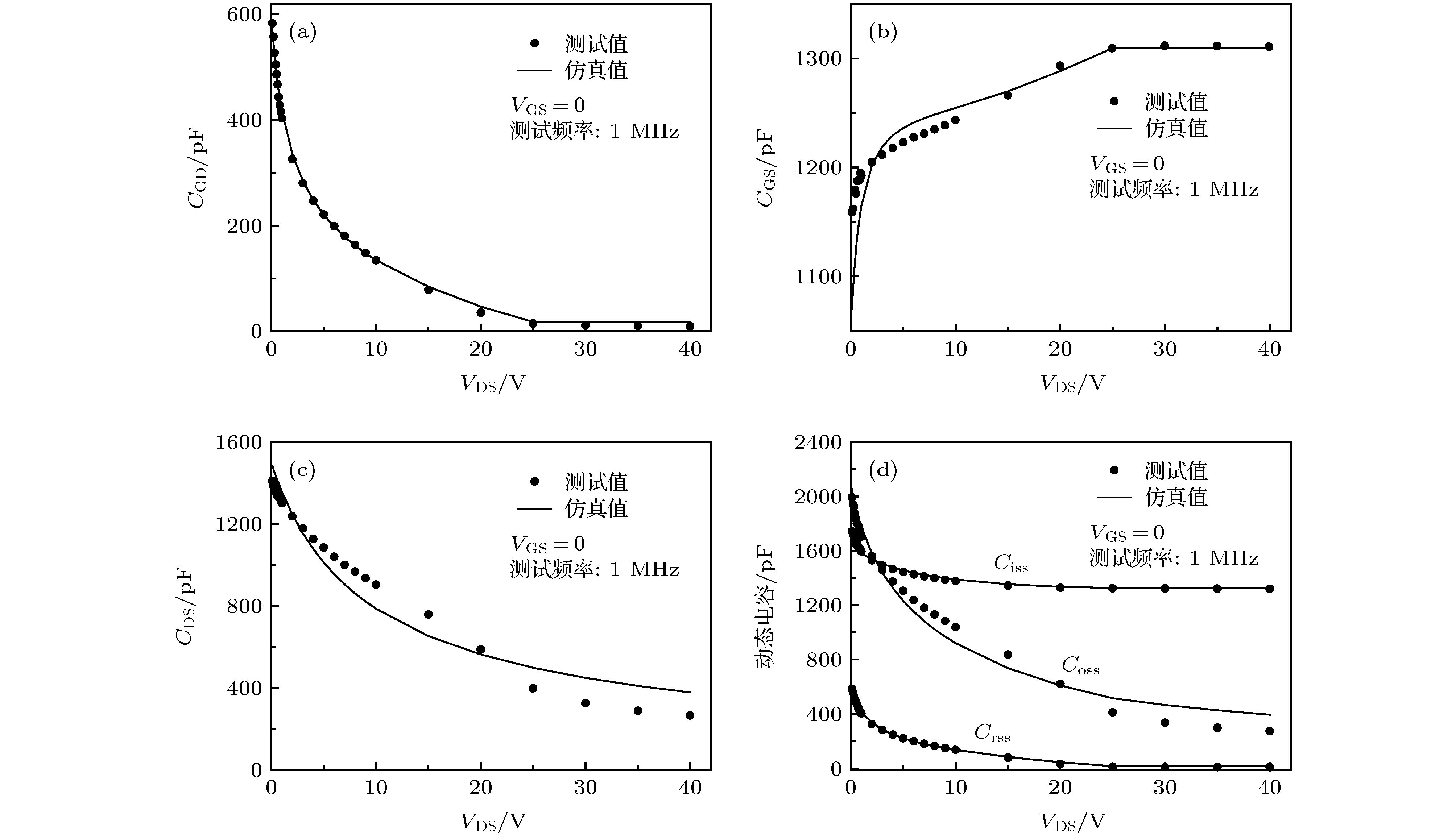
图 6 电容-偏压变化曲线 (a) CGD-VDS曲线; (b) CGS-VDS曲线; (c) CDS-VDS曲线; (d) Ciss, Coss, Crss关于VDS的曲线
Figure 6. Capacitance curves on bias voltage: (a) Curve of CGD on VDS; (b) curve of CGS on VDS; (c) curve of CDS on VDS; (d) curves of Ciss, Coss and Crss on VDS.

图 7 开关特性验证 (a) 测试电路; (b) 工作电流Ion = 10 A下的开关特性曲线
Figure 7. Verification of switching characteristic: (a) Switching characteristic test circuit; (b) switching characteristic curve at Ion = 10 A
表 1 SGT MOS的尺寸
Table 1. The size of SGT MOS.
参数名 含义 大小/μm tox 栅氧厚度 0.07 ti 屏蔽栅与漂移区间氧化层厚度 0.18 ts 槽右侧漂移区宽度 0.30 tDB 屏蔽栅底部与漂移区的距离 0.07 Lch 沟道长度 0.53 Lov 栅与漂移区重叠部分的长度 0.10 LDT 栅与屏蔽栅间距 0.52 LSH 屏蔽栅长度 0.87 Wcell 元胞宽度 1.20  DownLoad: CSV
-
[1] Wang Y, Hu H F, Yu C H, Wei J T 2015 IET Power Electronics 8 678
Google Scholar
[2] Sarkar T, Sapp S, Challa A 2013 28th Annual IEEE Applied Power Electronics Conference and Exposition (APEC) Long Beach, USA, March 17−21, 2013 p507
[3] Park C, Havanur S, Shibib A, Terrill K 2016 28th International Symposium on Power Semiconductor Devices and ICs (ISPSD) Prague, Czech Republic, June 12–16, 2016 p387
[4] Tong C F, Cortes I, Mawby P A, Covington J A, Morancho F 2009 IEEE Spanish Conference on Electron Devices Santiago de Compostela Santiago de Compostela, Spain, February 11–13, 2009 p250
[5] Choi W, Son D, Young S 2012 27th Annual IEEE Applied Power Electronics Conference and Exposition (APEC) Orlando, USA, February 5–9, 2012 p1676
[6] Wang Y, Yu C H, Li M S, Cao F, Liu Y J 2017 IEEE Trans. Electron Devices 64 1455
Google Scholar
[7] Bao J, Qi H, Zhang J, Zhang Y, Hao Z 2011 6th IEEE Joint International Information Technology and Artificial Intelligence Conference Chongqing, China, August 20–22, 2011 p245
[8] 王磊, 杨华岳 2010 物理学报 59 0571
Google Scholar
Wang L, Yang Y H 2010 Acta Phys. Sin. 59 0571
Google Scholar
[9] Shi L, Jia K, Sun W 2013 IEEE Trans. Electron Devices 60 346
Google Scholar
[10] Tanaka A, Oritsuki Y, Kikuchihara H, Miyake M 2011 IEEE Trans. Electron Devices 58 2072
Google Scholar
[11] Victory J, Pearson S, Benczkowski S, Sarkar T, Jang H, Yazdi M B, Mao K 2016 28th International Symposium on Power Semiconductor Devices and ICs Prague, Czech Republic, June 12–16, 2016 p219
[12] Xiao Y, Victory J, Pearson S, Sarkar T, Challa A, Dagan M, Collanton P, Andreev C 2019 34th Annual IEEE Applied Power Electronics Conference and Exposition Anaheim, USA, March 17–21, 2019 p508
[13] Xi X, Dunga M, He J, Liu W, Cao K M, Jin X, Ou J J, Chan M, Niknejad A M http://cmosedu.com/cmos1/BSIM4_manual. pdf[2020-1-28]
[14] 巴利伽 B J 著 (韩郑生, 陆江, 宋李梅译) 2013 功率半导体器件基础 (北京: 电子工业出版社) 第197—198页
Baliga B J (translated by Han Z S, Lu J, Song L M) 2013 Fundamentals of Power Semiconductor Devices (Beijing: Publishing House of Electronics Industry) pp197–198 (in Chinese)
[15] Klein P 1997 IEEE Trans. Electron Devices 44 1483
Google Scholar
[16] Daniel B J, Parikh C D, Patil M B 2002 IEEE Trans. Electron Devices 49 916
Google Scholar
[17] Arribas A P, Shang F, Krishnamurthy M, Shenai K 2015 IEEE Trans. Electron Devices 62 1449
Google Scholar
[18] Ren M, Chen Z, Niu B, Cao X, Li S, Li Z, Zhang B 2016 IEEE International Nanoelectronics Conference (INEC) Chengdu, China, May 9–11, 2016 p1
[19] Chauhan Y S, Gillon R, Declercq M, Ionescu A M 2007 37th European Solid State Device Research Conference Munich, Germany, September 11–13, 2007 p426
[20] Shenai K 1991 IEEE Trans. Power Electron 6 539
Google Scholar
[21] Agarwal H, Gupta C, Goel R, Kushwaha P, Lin Y K, Kao M Y, Duarte J P, Chang H L, Chauhan Y S, Salahuddin S, Hu C 2019 IEEE Trans. Electron Devices 66 4258
Google Scholar
[22] Zhang W T, Ye L, Fang D, Qiao M, Xiao K, He B, Li Z, Zhang B 2019 IEEE Trans. Electron Devices 66 1416
Google Scholar

 DownLoad:
Catalog
Metrics
- Abstract views: 7481
- PDF Downloads: 161
- Cited By: 0
