


-
Monolayer tellurene is a novel two-dimensional semiconductor with excellent intrinsic properties. It is helpful in understanding doping and scattering mechanism to study the electronic structure of defective tellurene, thus it is important for the application of tellurene in electronic and photo-electronic devices. Using first-principles calculation based on the density functional theory, we investigate the effects of commonly seen point defects on the electronic structure and optical properties of monolayer β-Te. Seven kinds of point defects that may be present in β-Te are designed according to the lattice symmetry, including two single vacancies (SV-1, SV-2), two double vacancies (DV-1, DV-2) and three Stone-Wales (SW) defects (SW-1, SW-2, SW-3). It is found that the defect formation energies of these defects are 0.83–2.06 eV, which are lower than that in graphene, silicene, phosphorene and arsenene, suggesting that they are easy to introduce into monolayer β-Te. The two most stable defects are SV-2 and SW-1 where no dangling bond emerges after optimization. The calculated band structures show that all seven defects have little effect on the band gap width of monolayer β-Te, but they can introduce different numbers of impurity energy levels into the forbidden band. Among them, the SV-1, SV-2, DV-1 and SW-2 each act as deep level impurities which can be recombination centers and scattering centers of carriers, SW-1 acts as a shallow level impurity, DV-2 and SW-3 act as both deep level impurity and shallow level impurity. Besides, SW-1, SW-2 and DV-1 can change the band gap of monolayer β-Te from direct band gap to indirect band gap, which may result in the increase of the lifetime of carriers and decrease of photoluminescence of monolayer β-Te. The optical properties of monolayer β-Te, which are sensitive to the change in band structure, are also affected by the presence of defects. New peaks are found in the complex dielectric function and the absorption coefficient of defective monolayer β-Te in an energy range of 0–3 eV, of which the number and the position are dependent on the type of defect. The SV-1, DV-1, DV-2 and SW-2 can enhance the light response, polarization ability and light absorption in the low energy region of monolayer β-Te. This research can provide useful guidance for the applications of β-Te in the electronic and optoelectronic devices.
-
Keywords:
- first-principle /
- defective tellurene /
- electronic structure /
- optical properties
[1] Novoselov K S, Geim A K, Morozov S V, Jiang D, Zhang Y, Dubonos S V, Grigorieva I V, Firsov A A 2004 Science 306 666
 Google Scholar
[2] Vogt P, De Padova P, Quaresima C, Avila J, Frantzeskakis E, Asensio M C, Resta A, Ealet B, Le Lay G 2012 Phys. Rev. Lett. 108 155501
Google Scholar
[3] 秦志辉 2017 物理学报 66 216802
Google Scholar
Qin Z J 2017 Acta Phys. Sin. 66 216802
Google Scholar
[4] Zhu F F, Chen W J, Xu Y, Gao C L, Guan D D, Liu C H, Qian D, Zhang S C, Jia J F 2015 Nat. Mater. 14 1020
Google Scholar
[5] Liu H, Neal A T, Zhu Z, Luo Z, Xu X, Tomanek D, Ye P D 2014 ACS Nano 8 4033
Google Scholar
[6] Ji J, Song X, Liu J, Yan Z, Huo C, Zhang S, Su M, Liao L, Wang W, Ni Z, Hao Y, Zeng H 2016 Nat. Commun. 7 13352
Google Scholar
[7] Manzeli S, Ovchinnikov D, Pasquier D, Yazyev O V, Kis A 2017 Nat. Rev. Mater. 2 17033
Google Scholar
[8] Radisavljevic B, Radenovic A, Brivio J, Giacometti V, Kis A 2011 Nat. Nanotechnol. 6 147
Google Scholar
[9] 顾品超, 张楷亮, 冯玉林, 王芳, 苗银萍, 韩叶梅, 张韩霞 2016 物理学报 65 018102
Google Scholar
Gu P C, Zhang K L, Feng Y L, Wang F, Miao Y P, Han Y M, Zhang H X 2016 Acta Phys. Sin. 65 018102
Google Scholar
[10] Zhu Z, Cai X, Yi S, Chen J, Dai Y, Niu C, Guo Z, Xie M, Liu F, Cho J H, Jia Y, Zhang Z 2017 Phys. Rev. Lett. 119 106101
Google Scholar
[11] Apte A, Bianco E, Krishnamoorthy A, Yazdi S, Rao R, Glavin N, Kumazoe H, Varshney V, Roy A, Shimojo F, Ringe E, Kalia R K, Nakano A, Tiwary C S, Vashishta P, Kochat V, Ajayan P M 2018 2D Mater. 6 015013
[12] Wang Y X, Qiu G, Wang R X, et al. 2018 Nat. Electron. 1 228
Google Scholar
[13] Wang Q, Safdar M, Xu K, Mirza M, Wang Z, He J 2014 ACS Nano 8 7497
Google Scholar
[14] Chen J, Dai Y, Ma Y, Dai X, Ho W, Xie M 2017 Nanoscale 9 15945
Google Scholar
[15] Xie Z, Xing C, Huang W, et al. 2018 Adv. Funct. Mater. 28 1705833
Google Scholar
[16] He Q, Liu Y, Tan C, Zhai W, Nam G-h, Zhang H 2019 ACS Nano 13 12294
Google Scholar
[17] Shi Z, Cao R, Khan K, et al. 2020 Nano-Micro Lett. 12 99
Google Scholar
[18] Qiao J, Pan Y, Yang F, Wang C, Chai Y, Ji W 2018 Sci. Bull. 63 159
Google Scholar
[19] Xu Y, Shi Z, Shi X, Zhang K, Zhang H 2019 Nanoscale 11 14491
Google Scholar
[20] Lim D, Kannan E S, Lee I, Rathi S, Li L, Lee Y, Khan M A, Kang M, Park J, Kim G-H 2016 Nanotechnology 27 225201
Google Scholar
[21] Hong S, Im H, Hong Y K, Liu N, Kim S, Park J H 2018 Adv. Electron. Mater. 4 1800308
Google Scholar
[22] Lv Y W, Liu Y, Qin W J, Chang S, Jiang C Z, Liu Y Y, Liao L 2019 IEEE T. Electron. Dev. 66 2365
Google Scholar
[23] Sharma S, Singh N, Schwingenschlogl U 2018 ACS Appl. Energ. Mater. 1 1950
Google Scholar
[24] Stone A J, Wales D J 1986 Chem. Phys. Lett. 128 501
Google Scholar
[25] Meyer J C, Kisielowski C, Erni R, Rossell M D, Crommie M F, Zettl A 2008 Nano. Lett. 8 3582
Google Scholar
[26] Zhou W, Zou X, Najmaei S, et al. 2013 Nano. Lett. 13 2615
Google Scholar
[27] 刘南舒, 周思, 赵纪军 2019 物理化学学报 35 1142
Google Scholar
Liu N S, Zhou S, Zhao J J 2019 Acta Phys. -Chim. Sin. 35 1142
Google Scholar
[28] 杨绍斌, 李思南, 沈丁, 唐树伟, 孙闻, 陈跃辉 2017 物理化学学报 33 520
Google Scholar
Yang S B, Li S N, Shen D, Tang S W, Sun W, Chen Y H 2017 Acta Phys. -Chim. Sin. 33 520
Google Scholar
[29] Zheng H L, Yang B S, Wang D D, Han R L, Du X B, Yan Y 2014 Appl. Phys. Lett. 104 132403
Google Scholar
[30] Cai Y Q, Zhou H B, Zhang G, Zhang Y W 2016 Chem. Mater. 28 8611
Google Scholar
[31] Li A, Pan J, Yang Z, Zhou L, Xiong X, Ouyang F 2018 J. Magn. Magn. Mater. 451 520
Google Scholar
[32] Dai X, Yang Z, Li A, Yang J, Ouyang F 2019 Superlattice Microst. 130 528
Google Scholar
[33] Wang X H, Wang D W, Yang A J, Koratkar N, Chu J F, Lv P L, Rong M Z 2018 Phys. Chem. Chem. Phys. 20 4058
Google Scholar
[34] Gao J, Zhang J, Liu H, Zhang Q, Zhao J 2013 Nanoscale 5 9785
Google Scholar
[35] Hu W, Yang J L 2015 J. Phys. Chem. C 119 20474
Google Scholar
[36] Liu X X, Liu L Z, Yang L, Wu X L, Chu P K 2016 J.Phys. Chem. C 120 24917
Google Scholar
[37] Gao J F, Zhang J F, Liu H S, Zhang Q F, Zhao J J 2013 Nanoscale. 5 9785
[38] Hu W, Yang J 2015 Phys. Chem. C 119 20474
[39] Liu X, Liu L, Yang L, Wu X, Chu P K 2016 J. Phys. Chem. C 120 24917
[40] Soler J M, Artacho E, Gale J D, et al. 2002 J. Phys.-Condens. Mat. 14 2745
Google Scholar
[41] Troullier N, Martins J L 1991 Phys. Rev. B 43 1993
Google Scholar
[42] Perdew J P, Burke K, Ernzerhof M 1996 Phys. Rev. Lett. 77 3865
Google Scholar
[43] Monkhorst H J, Pack J D 1976 Phys. Rev. B 13 5188
Google Scholar
[44] Reed M B 2009 Int. J. Comput. Math. 86 606
Google Scholar
[45] Ma J, Alfè D, Michaelides A, Wang E 2009 Phys. Rev. B 80 033407
[46] Banhart F, Kotakoski J, Krasheninnikov A V 2011 ACS Nano 5 26
Google Scholar
[47] Gajdoš M, Hummer K, Kresse G, Furthmüller J, Bechstedt F 2006 Phys. Rev. B 73 045112
Google Scholar
[48] Toll J S 1956 Phys. Rev. 104 1760
Google Scholar
[49] Wang V, Xiao W, Ma D M, Liu R J, Yang C M 2014 J. Appl. Phys. 115 043708
Google Scholar
-

图 1 优化后单层β-Te的俯视图和侧视图 (a) Perfect; (b) SV-1; (c) SV-2; (d) DV-1; (e) DV-2; (f) SW-1; (g) SW-2; (h) SW-3. 红色虚线矩形表示晶格常数为a和b的原胞, 黑色矩形表示第一布里渊区, 绿色标记缺陷附近的原子, 红色标记SW缺陷结构中的旋转键
Figure 1. Top and side views of optimized monolayer β-Te: (a) Perfect; (b) SV-1; (c) SV-2; (d) DV-1; (e) DV-2; (f) SW-1; (g) SW-2; (h) SW-3. The red dotted rectangle represents the unit cell with lattice constants a and b, and dark rectangle represents the first Brillouin zone. Green marks the atoms at the vicinity of defects, and red marks the rotating bonds in SW defects.

图 2 能带和态密度 (a) Perfect; (b) SV-1; (c) SV-2; (d) DV-1; (e) DV-2; (f) SW-1; (g) SW-2; (h) SW-3, 字母“f ”和红色数字分别标记缺陷能级和带隙
Figure 2. Band structure and density of states: (a) Perfect; (b) SV-1; (c) SV-2; (d) DV-1; (e) DV-2; (f) SW-1; (g) SW-2; (h) SW-3. The defect-induced energy levels and band gaps are marked by the label “f ” and red numbers, respectively.
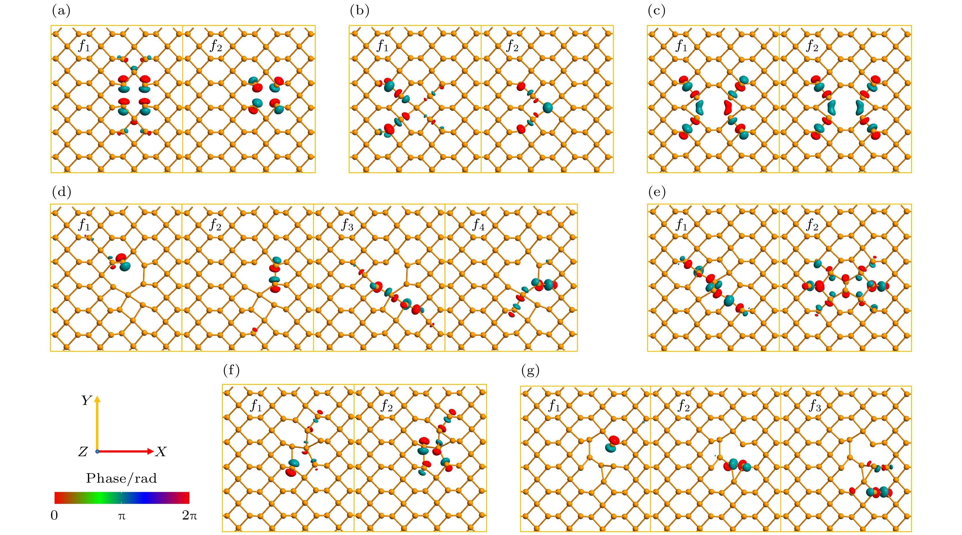
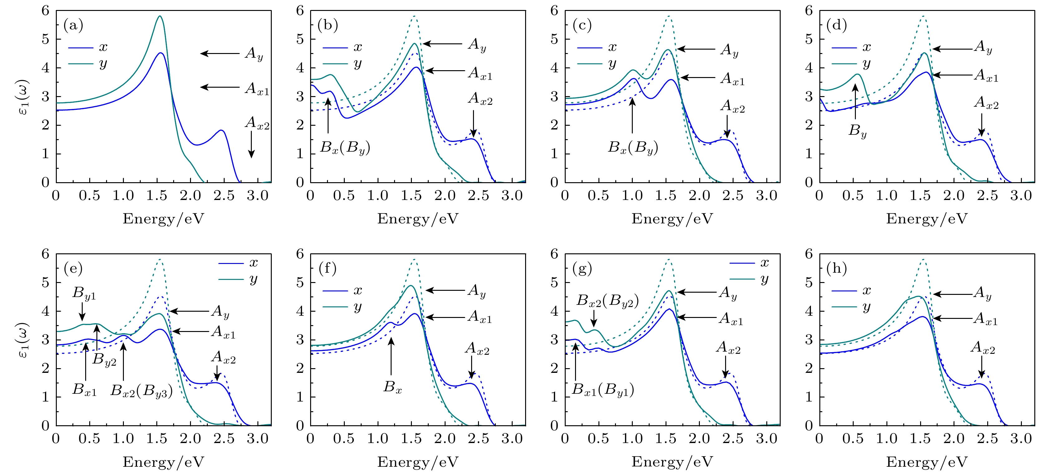
图 4 复介电函数实部 (a) Perfect; (b) SV-1; (c) SV-2; (d) DV-1; (e) DV-2; (f) SW-1; (g) SW-2; (h) SW-3, 蓝色和深青色分别表示x和y方向, A标记主峰, B标记缺陷峰, 虚线是完整单层的复介电函数实部
Figure 4. The real part of dielectric function: (a) Perfect; (b) SV-1; (c) SV-2; (d) DV-1; (e) DV-2; (f) SW-1; (g) SW-2; (h) SW-3. The blue and dark cyan curves represent x and y directions, respectively. The main peaks are marked by A and the defect-induced peaks are marked by B, and the dotted lines are the real part of dielectric function of perfect monolayer.
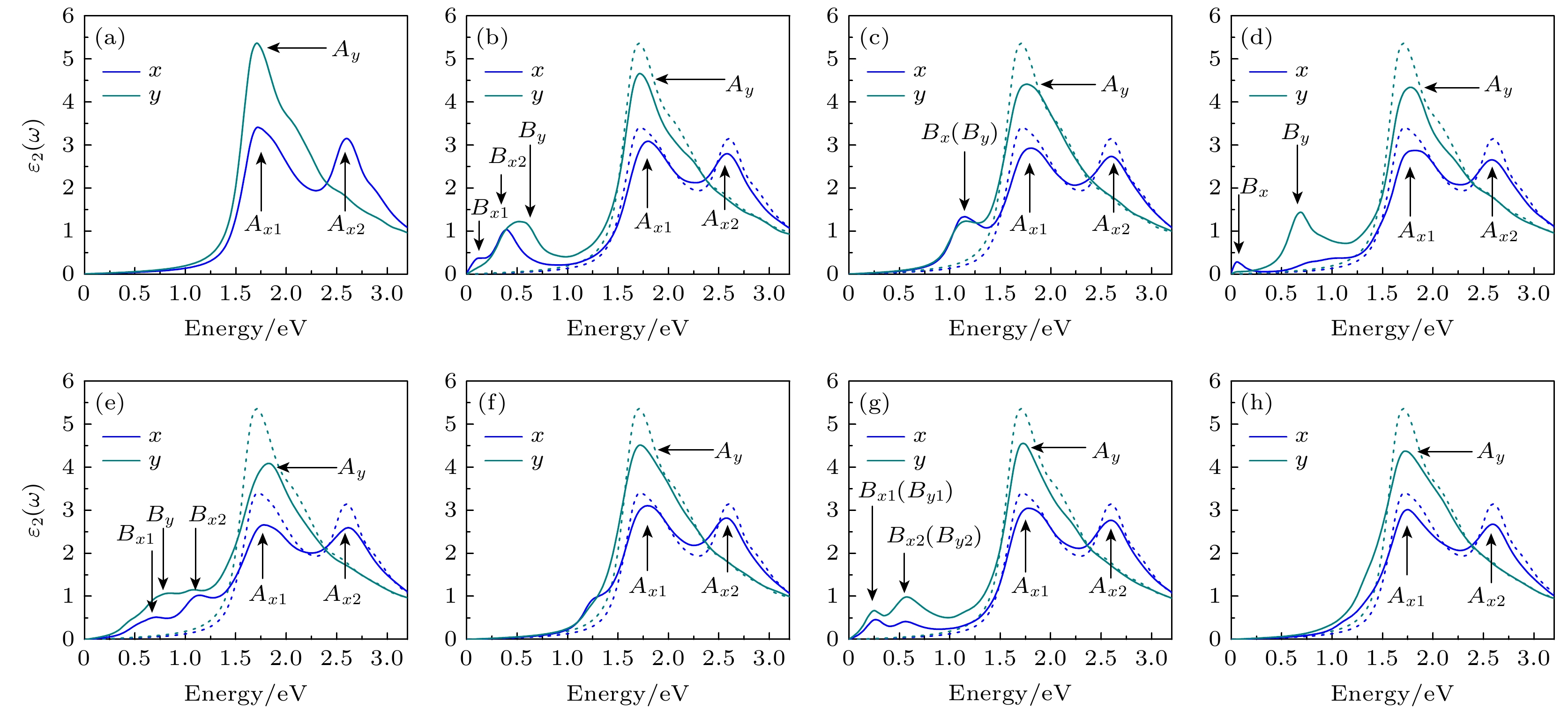
图 5 复介电函数虚部 (a) Perfect; (b) SV-1; (c) SV-2; (d) DV-1; (e) DV-2; (f) SW-1; (g) SW-2; (h) SW-3, 蓝色和深青色分别表示x和y方向, A标记主峰, B标记缺陷峰, 虚线是无缺陷的单层β-Te的复介电函数虚部
Figure 5. The imaginary part of dielectric function: (a) Perfect; (b) SV-1; (c) SV-2; (d) SW-1; (e) SW-2; (f) SW-3; (g) DV-1; (h) DV-2. The main peaks are marked by A and the defect-induced peaks are marked by B, and the dotted lines are the imaginary part of dielectric function of perfect monolayer.
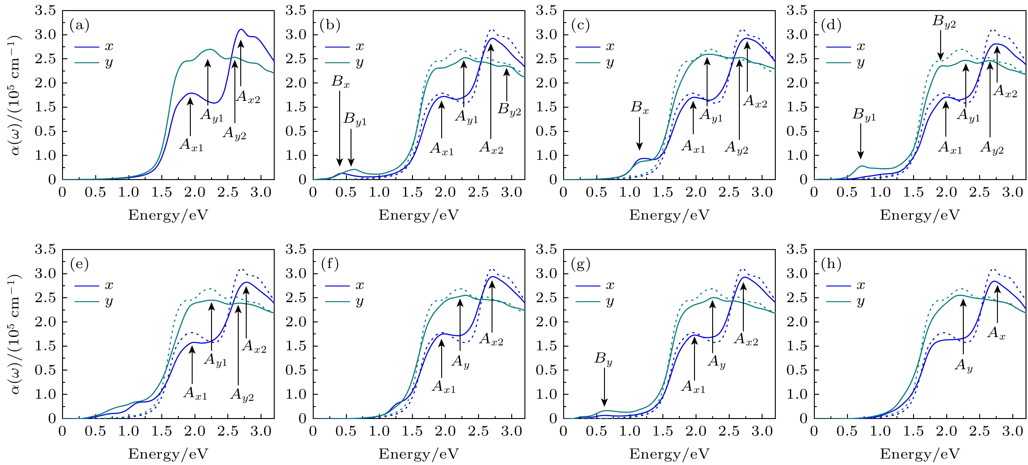
图 6 单层β-Te光学吸收系数 (a) Perfect; (b) SV-1; (c) SV-2; (d) DV-1; (e) DV-2; (f) SW-1; (g) SW-2; (h) SW-3. 蓝色和深青色分别表示x和y方向, A标记主峰, B标记缺陷峰, 虚线是完整单层的光学吸收系数
Figure 6. The optical absorption coefficient of monolayer β-Te: (a) Perfect; (b) SV-1; (c) SV-2; (d) DV-1; (e) DV-2; (f) SW-1; (g) SW-2; (h) SW-3. The main peaks are marked by A and the defect-induced peaks are marked by B, and the dotted lines are the optical absorption coefficient of perfect monolayer.
表 1 点缺陷形成能在单层β-Te与其他二维单质材料中的对比. 能量单位为eV.*
Table 1. The comparison of formation energies of various point defects in monolayer β-Te and other two-dimensional monoelemental materials. The unit of energy is eV.*
单质材料 SV-1 SV-2 SV-3 DV-1 DV-2 DV-3 SW-1 SW-2 SW-3 单层β-Te(本文) 1.37 0.85 — 2.06 1.59 — 0.83 1.50 1.53 石墨烯(本文) 8.15 — — 7.40 6.11 7.17 5.41 — — 石墨烯(Ref. [45,46]) 7.30—7.50 — — 7.20—7.90 6.40—7.50 7 4.50—5.30 — — 硅烯(Ref.[34]) 3.01 3.77 — 3.70 2.84 — 2.09 — — 磷烯(Ref. [35]) 1.63 2.03 — 1.91—3.04 2.08—2.61 2.13 1.01—1.32 — — 砷烯(Ref. [36]) 2.06—2.38 2.05—2.32 2.03—2.28 1.94—2.40 1.82—2.52 — 1.07—1.29 — — *注: 由于晶体结构不同, 各二维晶体中点缺陷的种类以及缺陷周围的原子排列存在差异. 表中的缺陷名称不代表唯一的结构, 具体缺陷结构需参考对应文献.  DownLoad: CSV
表 2 静态介电常数和复介电函数实部中缺陷峰的能量
Table 2. Static dielectric constant and defect peak energy coordinate of the real part curve.
perfect SV-1 SV-2 DV-1 DV-2 SW-1 SW-2 SW-3 静态介电常数 x方向 2.50 3.41 2.71 2.96 2.83 2.62 2.98 2.52 y方向 2.75 3.60 2.98 3.27 3.29 2.81 3.62 2.84 缺陷峰坐标/eV x方向 — 0.28 1.02 — 0.48, 1.01 1.21 0.19, 0.46 — y方向 — 0.28 1.02 0.58 0.38, 0.69, 1.01 — 0.19, 0.46 —
DownLoad: CSV
表 3 复介电函数虚部中缺陷峰的能量坐标
Table 3. Energies coordinates of defect-induced peaks in the imaginary part of dielectric function.
SV-1 SV-2 DV-1 DV-2 SW-2 x方向/eV 0.09, 0.39 1.12 0.06 0.71, 1.15 0.22, 0.55 y方向/eV 0.52 1.12 0.66 0.83 0.22, 0.55
DownLoad: CSV
表 4 光学吸收系数中缺陷峰的能量坐标和对应的跃迁
Table 4. Energies coordinates of defect-induced peaks in absorption coefficient and corresponding transition between energy levels.
缺
陷
峰x方向 y方向 能量/eV 对应跃迁 能量/eV 对应跃迁 SV-1 0.38 f1→f2 0.63 价带顶→f2 SV-2 1.12 价带顶→ f1、f2 — — DV-1 — — 0.72 价带顶→f2 SW-2 — — 0.62 f1→f2, 价带顶→f2
DownLoad: CSV
-
[1] Novoselov K S, Geim A K, Morozov S V, Jiang D, Zhang Y, Dubonos S V, Grigorieva I V, Firsov A A 2004 Science 306 666
Google Scholar
[2] Vogt P, De Padova P, Quaresima C, Avila J, Frantzeskakis E, Asensio M C, Resta A, Ealet B, Le Lay G 2012 Phys. Rev. Lett. 108 155501
Google Scholar
[3] 秦志辉 2017 物理学报 66 216802
Google Scholar
Qin Z J 2017 Acta Phys. Sin. 66 216802
Google Scholar
[4] Zhu F F, Chen W J, Xu Y, Gao C L, Guan D D, Liu C H, Qian D, Zhang S C, Jia J F 2015 Nat. Mater. 14 1020
Google Scholar
[5] Liu H, Neal A T, Zhu Z, Luo Z, Xu X, Tomanek D, Ye P D 2014 ACS Nano 8 4033
Google Scholar
[6] Ji J, Song X, Liu J, Yan Z, Huo C, Zhang S, Su M, Liao L, Wang W, Ni Z, Hao Y, Zeng H 2016 Nat. Commun. 7 13352
Google Scholar
[7] Manzeli S, Ovchinnikov D, Pasquier D, Yazyev O V, Kis A 2017 Nat. Rev. Mater. 2 17033
Google Scholar
[8] Radisavljevic B, Radenovic A, Brivio J, Giacometti V, Kis A 2011 Nat. Nanotechnol. 6 147
Google Scholar
[9] 顾品超, 张楷亮, 冯玉林, 王芳, 苗银萍, 韩叶梅, 张韩霞 2016 物理学报 65 018102
Google Scholar
Gu P C, Zhang K L, Feng Y L, Wang F, Miao Y P, Han Y M, Zhang H X 2016 Acta Phys. Sin. 65 018102
Google Scholar
[10] Zhu Z, Cai X, Yi S, Chen J, Dai Y, Niu C, Guo Z, Xie M, Liu F, Cho J H, Jia Y, Zhang Z 2017 Phys. Rev. Lett. 119 106101
Google Scholar
[11] Apte A, Bianco E, Krishnamoorthy A, Yazdi S, Rao R, Glavin N, Kumazoe H, Varshney V, Roy A, Shimojo F, Ringe E, Kalia R K, Nakano A, Tiwary C S, Vashishta P, Kochat V, Ajayan P M 2018 2D Mater. 6 015013
[12] Wang Y X, Qiu G, Wang R X, et al. 2018 Nat. Electron. 1 228
Google Scholar
[13] Wang Q, Safdar M, Xu K, Mirza M, Wang Z, He J 2014 ACS Nano 8 7497
Google Scholar
[14] Chen J, Dai Y, Ma Y, Dai X, Ho W, Xie M 2017 Nanoscale 9 15945
Google Scholar
[15] Xie Z, Xing C, Huang W, et al. 2018 Adv. Funct. Mater. 28 1705833
Google Scholar
[16] He Q, Liu Y, Tan C, Zhai W, Nam G-h, Zhang H 2019 ACS Nano 13 12294
Google Scholar
[17] Shi Z, Cao R, Khan K, et al. 2020 Nano-Micro Lett. 12 99
Google Scholar
[18] Qiao J, Pan Y, Yang F, Wang C, Chai Y, Ji W 2018 Sci. Bull. 63 159
Google Scholar
[19] Xu Y, Shi Z, Shi X, Zhang K, Zhang H 2019 Nanoscale 11 14491
Google Scholar
[20] Lim D, Kannan E S, Lee I, Rathi S, Li L, Lee Y, Khan M A, Kang M, Park J, Kim G-H 2016 Nanotechnology 27 225201
Google Scholar
[21] Hong S, Im H, Hong Y K, Liu N, Kim S, Park J H 2018 Adv. Electron. Mater. 4 1800308
Google Scholar
[22] Lv Y W, Liu Y, Qin W J, Chang S, Jiang C Z, Liu Y Y, Liao L 2019 IEEE T. Electron. Dev. 66 2365
Google Scholar
[23] Sharma S, Singh N, Schwingenschlogl U 2018 ACS Appl. Energ. Mater. 1 1950
Google Scholar
[24] Stone A J, Wales D J 1986 Chem. Phys. Lett. 128 501
Google Scholar
[25] Meyer J C, Kisielowski C, Erni R, Rossell M D, Crommie M F, Zettl A 2008 Nano. Lett. 8 3582
Google Scholar
[26] Zhou W, Zou X, Najmaei S, et al. 2013 Nano. Lett. 13 2615
Google Scholar
[27] 刘南舒, 周思, 赵纪军 2019 物理化学学报 35 1142
Google Scholar
Liu N S, Zhou S, Zhao J J 2019 Acta Phys. -Chim. Sin. 35 1142
Google Scholar
[28] 杨绍斌, 李思南, 沈丁, 唐树伟, 孙闻, 陈跃辉 2017 物理化学学报 33 520
Google Scholar
Yang S B, Li S N, Shen D, Tang S W, Sun W, Chen Y H 2017 Acta Phys. -Chim. Sin. 33 520
Google Scholar
[29] Zheng H L, Yang B S, Wang D D, Han R L, Du X B, Yan Y 2014 Appl. Phys. Lett. 104 132403
Google Scholar
[30] Cai Y Q, Zhou H B, Zhang G, Zhang Y W 2016 Chem. Mater. 28 8611
Google Scholar
[31] Li A, Pan J, Yang Z, Zhou L, Xiong X, Ouyang F 2018 J. Magn. Magn. Mater. 451 520
Google Scholar
[32] Dai X, Yang Z, Li A, Yang J, Ouyang F 2019 Superlattice Microst. 130 528
Google Scholar
[33] Wang X H, Wang D W, Yang A J, Koratkar N, Chu J F, Lv P L, Rong M Z 2018 Phys. Chem. Chem. Phys. 20 4058
Google Scholar
[34] Gao J, Zhang J, Liu H, Zhang Q, Zhao J 2013 Nanoscale 5 9785
Google Scholar
[35] Hu W, Yang J L 2015 J. Phys. Chem. C 119 20474
Google Scholar
[36] Liu X X, Liu L Z, Yang L, Wu X L, Chu P K 2016 J.Phys. Chem. C 120 24917
Google Scholar
[37] Gao J F, Zhang J F, Liu H S, Zhang Q F, Zhao J J 2013 Nanoscale. 5 9785
[38] Hu W, Yang J 2015 Phys. Chem. C 119 20474
[39] Liu X, Liu L, Yang L, Wu X, Chu P K 2016 J. Phys. Chem. C 120 24917
[40] Soler J M, Artacho E, Gale J D, et al. 2002 J. Phys.-Condens. Mat. 14 2745
Google Scholar
[41] Troullier N, Martins J L 1991 Phys. Rev. B 43 1993
Google Scholar
[42] Perdew J P, Burke K, Ernzerhof M 1996 Phys. Rev. Lett. 77 3865
Google Scholar
[43] Monkhorst H J, Pack J D 1976 Phys. Rev. B 13 5188
Google Scholar
[44] Reed M B 2009 Int. J. Comput. Math. 86 606
Google Scholar
[45] Ma J, Alfè D, Michaelides A, Wang E 2009 Phys. Rev. B 80 033407
[46] Banhart F, Kotakoski J, Krasheninnikov A V 2011 ACS Nano 5 26
Google Scholar
[47] Gajdoš M, Hummer K, Kresse G, Furthmüller J, Bechstedt F 2006 Phys. Rev. B 73 045112
Google Scholar
[48] Toll J S 1956 Phys. Rev. 104 1760
Google Scholar
[49] Wang V, Xiao W, Ma D M, Liu R J, Yang C M 2014 J. Appl. Phys. 115 043708
Google Scholar

 DownLoad:
Catalog
Metrics
- Abstract views: 5107
- PDF Downloads: 211
- Cited By: 0
