


-
Two-dimensional topological insulator (2DTI) with a large bandgap is prerequisite for potentially observing quantum spin Hall and other quantum phenomena at room-temperature. At present, the synthesis of such materials possesses formidable challenge. In this work, we report our experimental results on synthesis of large-gap 2DTI stanene and bismuthene on B-faced InSb(111) substrate by using molecular beam epitaxy technology. We find that both the stanene and bismuthene can be synthesized by following the forming of a wetting layer on InSb(111) substrate, but with different prospects. On the one hand, it is found that the binding energy between Sn and the substrate is not strong enough to compete the binding force between Sn atoms during the post annealing, thus resulting in a wetting layer composed of many small domains. It significantly restricts the quality of the stanene epilayers. On the other hand, the Bi atoms on InSb(111) are found more stable than the Sn atoms on InSb(111), resulting in a uniform wetting layer which can be optimized by adjusting substrate temperature and post-annealing conditions. Large size and single crystal bismuthene domains have been observed under the STM measurement, which also indicates a bulk gap of ~0.15 eV and metallic edge states.
-
Keywords:
- low-dimensional topological insulator /
- stanene /
- bismuthene /
- molecular beam epitaxy
[1] Aasen D, Hell M, Mishmash R V, Higginbotham A, Danon J, Leijnse M, Jespersen T S, Folk J A, Marcus C M, Flensberg K, Alicea J 2016 Phys. Rev. X 6 031016
 Google Scholar
[2] Hsu C H, Stano P, Klinovaja J, Loss D 2018 Phys. Rev. Lett. 121 196801
Google Scholar
[3] Liu C, Jia J F 2014 Natl. Sci. Rev. 1 36
Google Scholar
[4] Shen S Q 2017 Springer Series in Solid-State Sciences (Singapore: Springer) pp189–206
[5] Bernevig B A, Hughes T L, Zhang S C 2006 Science 314 1757
Google Scholar
[6] König M, Wiedmann S, Brüne C, Roth A, Buhmann H, Molenkamp L W, Qi X L, Zhang S C 2007 Science 318 766
Google Scholar
[7] Knez I, Du R R, Sullivan G 2011 Phys. Rev. Lett. 107 136603
Google Scholar
[8] Kou L, Ma Y, Sun Z, Heine T, Chen C 2017 J. Phys. Chem. Lett. 8 1905
Google Scholar
[9] Vergniory M G, Elcoro L, Felser C, Regnault N, Bernevig B A, Wang Z 2019 Nature 566 480
Google Scholar
[10] Zhang T, Jiang Y, Song Z, Huang H, He Y, Fang Z, Weng H, Fang C 2019 Nature 566 475
Google Scholar
[11] Deng J, Xia B, Ma X, Chen H, Shan H, Zhai X, Li B, Zhao A, Xu Y, Duan W, Zhang S C, Wang B, Hou J G 2018 Nat. Mater. 17 1081
Google Scholar
[12] Evazzade I, Roknabadi M R, Morshedloo T, Modarresi M, Mogulkoc Y, Nemati Far H 2017 Physica E 89 155
Google Scholar
[13] Liao M, Zang Y, Guan Z, Li H, Gong Y, Zhu K, Hu X P, Zhang D, Xu Y, Wang Y Y, He K, Ma X C, Zhang S C, Xue Q K 2018 Nat. Phys. 14 344
Google Scholar
[14] Zhu F, Chen W, Xu Y, Gao C, Guan D, Liu C, Qian D, Zhang S C, Jia J 2015 Nat. Mater. 14 1020
Google Scholar
[15] Aktürk E, Aktürk O Ü, Ciraci S 2016 Phys. Rev. B 94 014115
Google Scholar
[16] Reis F, Li G, Dudy L, Bauernfeind M, Glass S, Hanke W, Thomale R, Schäfer J, Claessen R 2017 Science 357 287
Google Scholar
[17] Zhou D, Yang C, Bu S, Pan F, Si N, He P, Ji Q, Lu Y, Niu T 2021 Phys. Rev. Mater. 5 064002
Google Scholar
[18] Deng Y, Yu Y, Shi M Z, Guo Z, Xu Z, Wang J, Chen X H, Zhang Y 2020 Science 367 895
Google Scholar
[19] Ning W, Mao Z 2020 APL Mater. 8 090701
Google Scholar
[20] Liu D F, Liang A J, Liu E K, Xu Q N, Li Y W, Chen C, Pei D, Shi W J, Mo S K, Dudin P, Kim T, Cacho C, Li G, Sun Y, Yang L X, Liu Z K, Parkin S S P, Felser C, Chen Y L 2019 Science 365 1282
Google Scholar
[21] Tokura Y, Yasuda K, Tsukazaki A 2019 Nat. Rev. Phys. 1 126
Google Scholar
[22] Saxena S, Chaudhary R P, Shukla S 2016 Sci. Rep. 6 31073
Google Scholar
[23] Zheng X, Zhang J F, Tong B, Du R R 2019 2D Mater. 7 011001
Google Scholar
[24] Song Y H, Wang Z W, Jia Z Y, Zhu X Y, Shi Z Q, Zhu L, Yuan Q Q, Shu D J, Li S C 2021 J. Phys. D: Appl. Phys. 54 304002
Google Scholar
[25] Xu Y, Yan B, Zhang H J, Wang J, Xu G, Tang P, Duan W, Zhang S C 2013 Phys. Rev. Lett. 111 136804
Google Scholar
[26] Gonze X, Michenaud J P, Vigneron J P 1990 Phys. Rev. B 41 11827
Google Scholar
[27] Kriegner D, Panse C, Mandl B, Dick K A, Keplinger M, Persson J M, Caroff P, Ercolani D, Sorba L, Bechstedt F, Stangl J, Bauer G 2011 Nano Lett. 11 1483
Google Scholar
[28] Chakraborty B, Borgohain M M, Adhikary N C 2020 Mater. Res. Express 7 015029
Google Scholar
[29] Zhao C, Jia J 2020 Front. Phys. 15 53201
Google Scholar
[30] Wang X, Shen N, Yang X, Wang B 2020 J. Cryst. Growth 546 125787
Google Scholar
[31] Xu C Z, Chan Y H, Chen P, Wang X, Flötotto D, Hlevyack J A, Bian G, Mo S K, Chou M Y, Chiang T C 2018 Phys. Rev. B 97 035122
Google Scholar
[32] Xu Y, Tang P, Zhang S C 2015 Phys. Rev. B 92 081112
Google Scholar
[33] Yuhara J, Fujii Y, Nishino K, Isobe N, Nakatake M, Xian L, Rubio A, Lay G L 2018 2D Mater. 5 025002
Google Scholar
[34] Falson J, Xu Y, Liao M, Zang Y, Zhu K, Wang C, Zhang Z, Liu H, Duan W, He K, Liu H, Smet J H, Zhang D, Xue Q K 2020 Science 367 1454
Google Scholar
[35] Lu Y, Xu W, Zeng M, Yao G, Shen L, Yang M, Luo Z, Pan F, Wu K, Das T, He P, Jiang J, Martin J, Feng Y P, Lin H, Wang X 2015 Nano Lett. 15 80
Google Scholar
[36] Nagao T, Sadowski J T, Saito M, Yaginuma S, Fujikawa Y, Kogure T, Ohno T, Hasegawa Y, Hasegawa S, Sakurai T 2004 Phys. Rev. Lett. 93 105501
Google Scholar
[37] Liu Z, Liu C X, Wu Y S, Duan W H, Liu F, Wu J 2011 Phys. Rev. Lett. 107 136805
Google Scholar
-
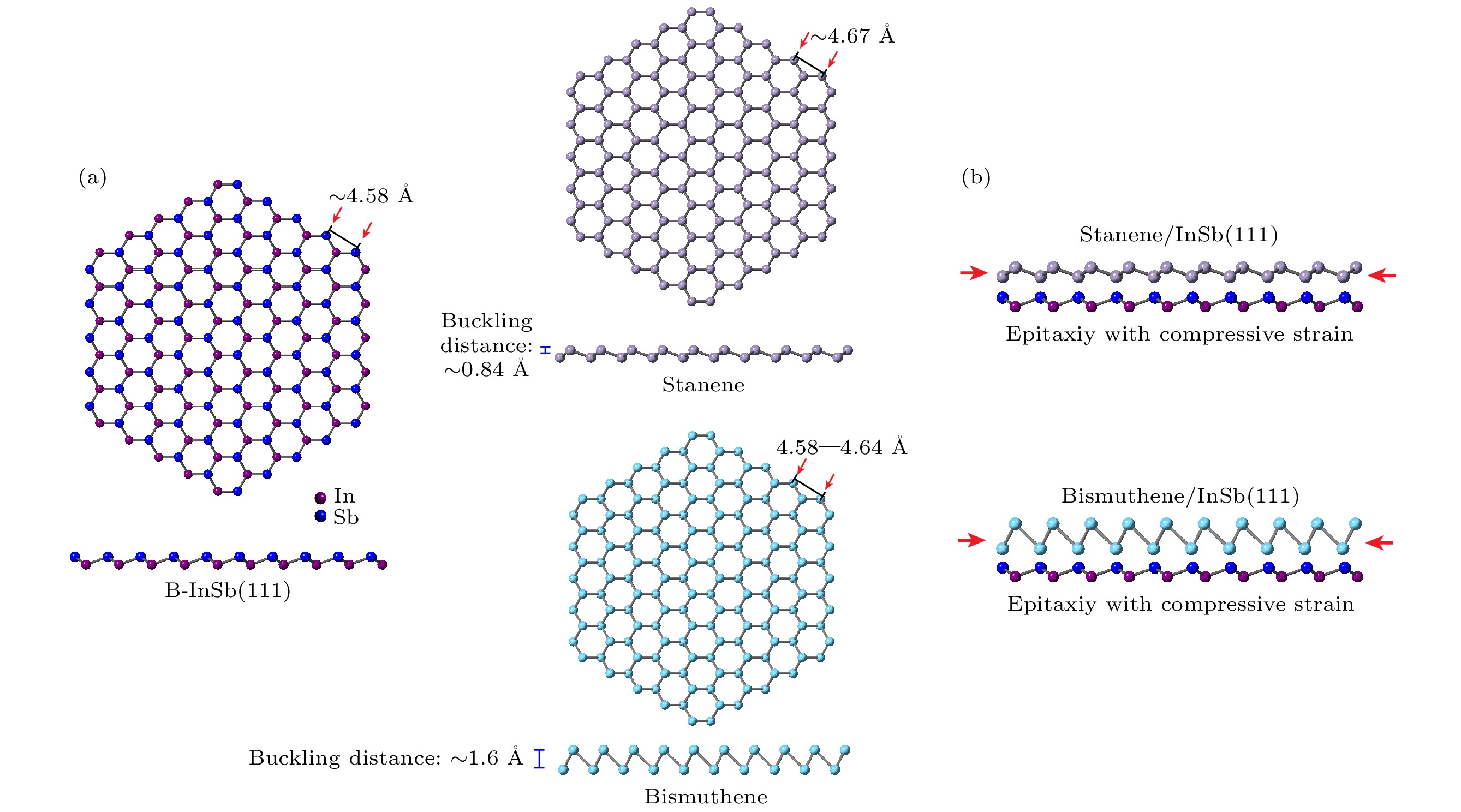
图 1 (a) InSb(111)、锡烯以及铋烯的晶格结构的平面以及侧视图, 参考理论计算文献可知三者的晶格常数分别约为4.58 Å[27], 4.67 Å[24,25]以及4.58—4.64 Å[15,26]; 二维锡烯与铋烯具有显著的翘曲结构, 其中锡烯的翘曲高度为0.84 Å[28], 铋烯的翘曲高度约为1.6 Å[15]; (b) 基于InSb(111)外延锡烯与铋烯的示意图
Figure 1. (a) In-plane and side view of the InSb(111) surface, stanene and bismuthene atomic structures; their lattice constants referred to the calculation works are 4.58 Å[27], 4.67 Å[24,25], and 4.58–4.64 Å[15,26], respectively; the 2D topological insulator stanene and bismuthene are bulked with a height of 0.84 Å[28] for stanene and ~1.6 Å[15] for bismuthene; (b) schematic of the lattice alignments of epitaxial growth of stanene and bismuthene on InSb(111) substrate.
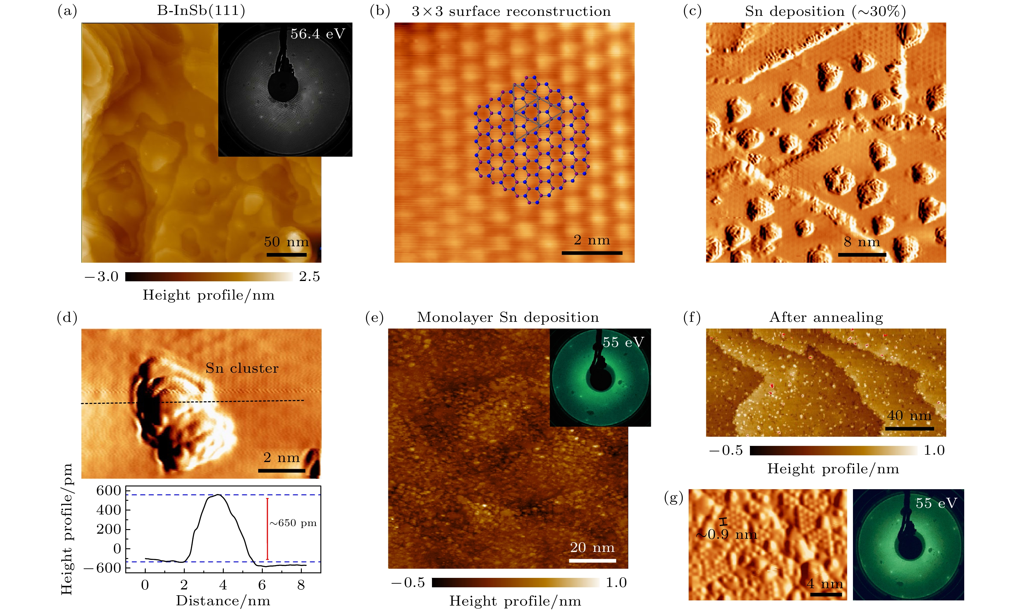
图 2 (a) 经过500 eV Ar离子轰击及380 ℃退火处理的InSb(111)表面的STM形貌图及LEED测量结果, 在LEED结果中绿色圆圈标识了InSb(111)晶格所对应的衍射斑点, 红色圈出的衍射点证实了表面存在的
$ 3\times 3 $ 原子重构; (b) 原子分辨的InSb(111)衬底表面晶格成像, 直观清晰地呈现了表面重构的原子结构; (c) 少量Sn原子(930 ℃, 5 min)在室温下沉积到衬底上的STM形貌图, 成核点逐渐形成岛状结构; (d) 上: 放大显示的Sn原子构成的岛状结构, 下: 岛状结构的高度为单原子层; (e) 当接近一层的Sn原子(930 ℃, 15 min)沉积到InSb(111)衬底后的表面形貌, 显示原子排列较为杂乱, 并未形成晶体学薄膜; LEED衍射斑点显示衬底的晶格特征, 其中衬底重构消失; (f) 对图(e)中的样品进行230 ℃真空退火后的薄膜相貌, 显示平整度显著提升; (g) 左图: 高分辨测量显示三角形晶畴形成, 但并不连续, 存在明显的缺陷, 晶格常数约为9 Å; 右图: 退火后样品的LEED衍射结构没有显著变化. STM测试条件: 测量温度为77 K; 样品偏压为600 mV; 阈值电流为200 pAFigure 2. (a) STM morphology of InSb(111) substrate that has been processed with 500 eV Ar ion bombardment following with annealing at 380 ℃; the inset shows the LEED pattern acquired at 56.4 eV, which presents the diffraction points (red circles) of the
$ 3\times 3 $ surface reconstruction, green circles reveal the lattice of InSb(111) surface; (b) atomic-resolved STM image of the InSb(111) where the surface reconstruction can be directly observed; (c) STM image of the InSb(111) surface after Sn atoms being deposited (930 ℃, 5 min), Sn islands can be observed; (d) up panel: STM image of a single Sn island; down panel: height profile of the island; (e) STM morphology of the surface with monolayer Sn atoms deposited, there is no clear atom structure, and the LEED pattern inset shows the surface reconstruction disappears; (f) STM morphology presents the surface evolution after 230 ℃ annealing in the vacuum; (g) left: high-resolution STM image shows the noncontinuous domains and defects in the Sn-wetting layer; right: LEED patterns of the annealed sample. STM parameters: T = 77 K, sample bias = 600 mV, setpoint current = 200 pA.
图 3 (a) 浸润层上第一层Sn沉积约为90%时退火后样品的STM形貌图, 不同尺寸的视野显示薄膜具有岛状生长的特征, 并且除了存在大量空隧道外表面还存在大量原子吸附; (b) 当Sn原子沉积接近100%时, STM图像显示薄膜变得连续但仍然存在由于晶畴拼接导致的三角形缺陷, 且三角形具有相同的取向; 放大的STM图像显示薄膜由大量4—6 nm小晶畴构成, 畴壁处的缺陷导致原子吸附; (c) 当第3层Sn原子沉积并退火后, 大量小晶畴拼接薄膜的行为越发明显, 从小晶畴的晶格形貌与理想锡烯对比, 发现这些小晶畴为锡烯单晶. STM测试条件: 测量温度为4.2 K; 样品偏压为1.5 V; 阈值电流为1.5 nA
Figure 3. (a) STM images of the annealed sample after about 90% Sn atoms being deposited on the Sn wetting layer, the high-resolution STM image in the right panel shows the adatoms and defects; (b) STM images of the sample with 100% Sn atoms deposited on the wetting layer shows the continuous film with some triangle defects, the high-resolution image in the right panel shows the film is composed by many small domains (4–6 nm) with defects on the domain walls; (c) STM images shows the third layer Sn-film is formed when the sample is annealed with enough Sn atoms being deposited; the film is obviously formed by many small domains, and the lattice structure of the domains fit the lattice of stanene very well. STM parameters: Temperature = 4.2 K, sample bias = 1.5 V, setpoint current = 1.5 nA
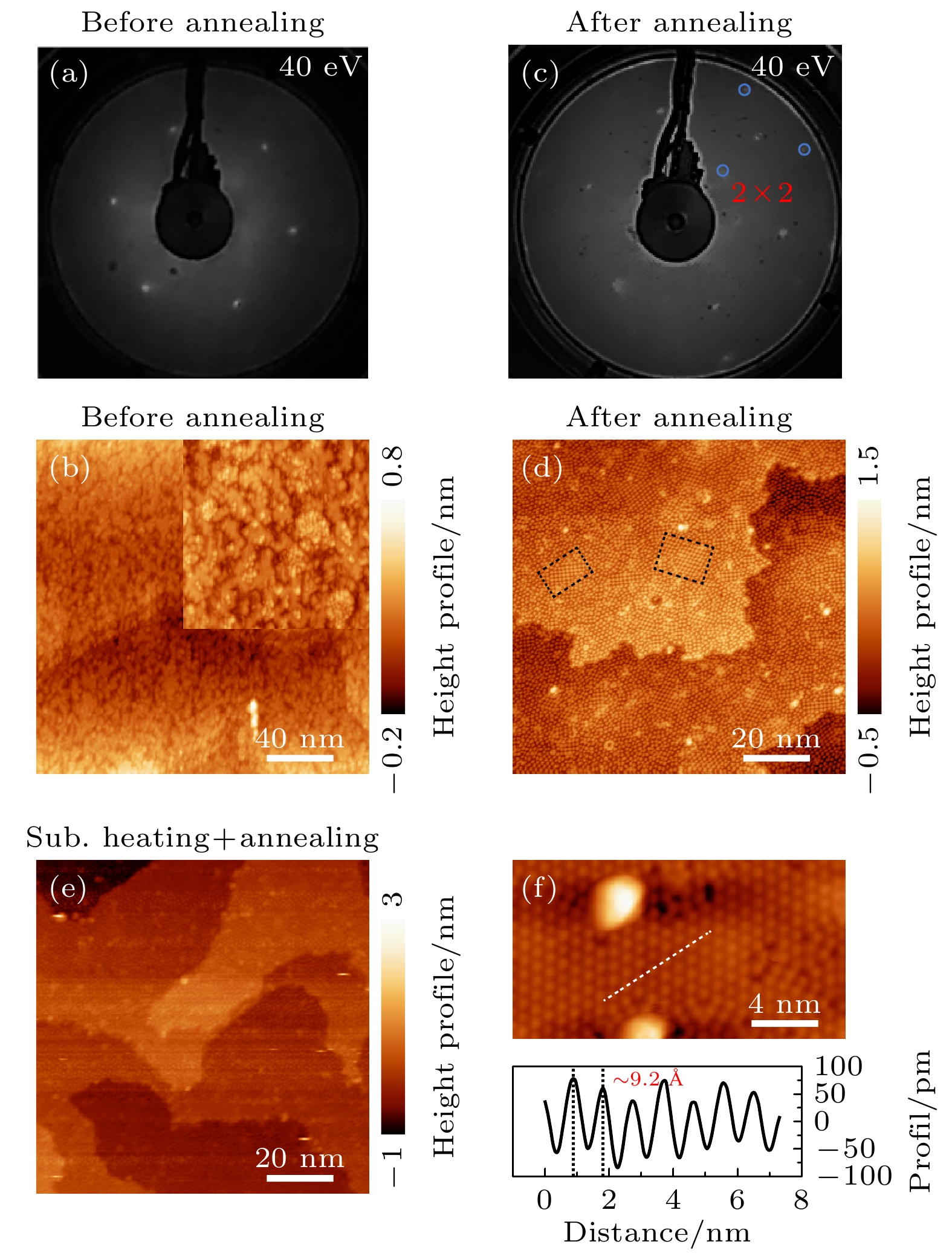
图 4 (a), (b) 单层铋原子沉积到InSb(111)衬底后, LEED以及STM结果, 其中LEED衍射斑点显示InSb(111)衬底的原子重构消失; (c), (d) 同一样品逐渐升温至350 ℃退火30 min后的LEED及STM测量结果, 其中在图(c)中隐约能够观测到Bi膜
$ 2\times 2 $ 重构所导致的衍射斑点; (d) 图中用虚线框出了出现四方结构的区域; (e) 当衬底温度为300 ℃时, 沉积单层铋原子并退火后形成连续且匀质的浸润层STM形貌图; (f) 原子分辨的STM形貌显示浸润层存在$ 2\times 2 $ 原子重构, 沿着图中白线获得的浸润层轮廓线显示浸润层的晶格常数约为9.2 Å. STM测试条件: 测量温度为77 K; 样品偏压为1 V; 阈值电流为500 pAFigure 4. (a), (b) LEED and STM image of sample with monolayer Bi atoms are deposited on InSb(111) substrate; LEED pattern shows the
$ 3\times 3 $ surface reconstruction disappears after deposition of Bi atoms; (c), (d) the same sample as that in panel (a) and (b) but after being annealed at 350 ℃ for 30 min;$ 2\times 2 $ surface reconstruction can be distinguished in the LEED pattern; and the region with black dashed squares show the tetragonal lattice; (e) STM morphology of the sample with both post-annealing and heating of substrate at 300 ℃ during deposition of Bi atoms, which shows uniform Bi film; (f) up panel: high-resolution STM image of the first Bi layer on InSb(111); down panel: the profile along the white dashed line in the up panel show the lattice constant is about 9.2 Å. STM parameters: Temperature = 77 K, sample bias = 1 V, setpoint current = 500 pA.
图 5 (a) STM形貌图显示浸润层上生长出具有规则边缘的1层(2-Bi)及2层(3-Bi)锡烯单晶; (b) 1层锡烯膜的厚度约为550 pm; (c) 第二层(3-Bi)的铋烯的原子形貌图, 其中薄膜中普遍存在原子空位缺陷; 对比可以看出单晶薄膜完好匹配理想锡烯的晶格结构; (d) 3-Bi锡烯层的晶格常数约为4.5 Å; (e) 液氮温度下浸润层dI/dV谱, 通过对浸润层上多点谱线进行平均显示浸润层具有稳定的带隙, 约为0.3 eV; (f) 在3-Bi上((c)中右图星形及圆形标示位置)获取的dI/dV谱线, 显示其体态具有约为0.15 eV的能带隙而边缘处为无能隙状态, 符合拓扑绝缘体边缘态的特征. STM测试条件: 测量温度为77 K; 样品偏压为1 V; 阈值电流为500 pA. STS: 锁相频率为707 Hz, 调制电压为8 mV
Figure 5. (a) STM image captured on a region containing wetting layer, the first bismuthene layer (2-Bi) and the second bismuthene layer (3-Bi); the bismuthene domain has very sharp edges; (b) line profile across 2-Bi and the wetting layer shows the thickness of bismuthene monolayer is about 550 pm; (c) left: atomic-resolved STM image on 3-Bi film shows the vacancies, and in the right panel comparison between the lattice of 3-Bi and the lattice model of bismuthene shows good consistency; (d) profile along the white dashed line in panel (c) shows the lattice constant of bismuthene is about 4.5 Å; (e), (f) the tunneling spectra which reveal the surface density of states acquired on the wetting layer and the 3-Bi layer; it shows the gapless edge state at the edge of the 3-Bi layer compared with that on the bulk. STM parameters: Temperature = 77 K, sample bias = 1 V, setpoint current = 500 pA. STS: lock-in frequency = 707 Hz, modulation voltage = 8 mV.
-
[1] Aasen D, Hell M, Mishmash R V, Higginbotham A, Danon J, Leijnse M, Jespersen T S, Folk J A, Marcus C M, Flensberg K, Alicea J 2016 Phys. Rev. X 6 031016
Google Scholar
[2] Hsu C H, Stano P, Klinovaja J, Loss D 2018 Phys. Rev. Lett. 121 196801
Google Scholar
[3] Liu C, Jia J F 2014 Natl. Sci. Rev. 1 36
Google Scholar
[4] Shen S Q 2017 Springer Series in Solid-State Sciences (Singapore: Springer) pp189–206
[5] Bernevig B A, Hughes T L, Zhang S C 2006 Science 314 1757
Google Scholar
[6] König M, Wiedmann S, Brüne C, Roth A, Buhmann H, Molenkamp L W, Qi X L, Zhang S C 2007 Science 318 766
Google Scholar
[7] Knez I, Du R R, Sullivan G 2011 Phys. Rev. Lett. 107 136603
Google Scholar
[8] Kou L, Ma Y, Sun Z, Heine T, Chen C 2017 J. Phys. Chem. Lett. 8 1905
Google Scholar
[9] Vergniory M G, Elcoro L, Felser C, Regnault N, Bernevig B A, Wang Z 2019 Nature 566 480
Google Scholar
[10] Zhang T, Jiang Y, Song Z, Huang H, He Y, Fang Z, Weng H, Fang C 2019 Nature 566 475
Google Scholar
[11] Deng J, Xia B, Ma X, Chen H, Shan H, Zhai X, Li B, Zhao A, Xu Y, Duan W, Zhang S C, Wang B, Hou J G 2018 Nat. Mater. 17 1081
Google Scholar
[12] Evazzade I, Roknabadi M R, Morshedloo T, Modarresi M, Mogulkoc Y, Nemati Far H 2017 Physica E 89 155
Google Scholar
[13] Liao M, Zang Y, Guan Z, Li H, Gong Y, Zhu K, Hu X P, Zhang D, Xu Y, Wang Y Y, He K, Ma X C, Zhang S C, Xue Q K 2018 Nat. Phys. 14 344
Google Scholar
[14] Zhu F, Chen W, Xu Y, Gao C, Guan D, Liu C, Qian D, Zhang S C, Jia J 2015 Nat. Mater. 14 1020
Google Scholar
[15] Aktürk E, Aktürk O Ü, Ciraci S 2016 Phys. Rev. B 94 014115
Google Scholar
[16] Reis F, Li G, Dudy L, Bauernfeind M, Glass S, Hanke W, Thomale R, Schäfer J, Claessen R 2017 Science 357 287
Google Scholar
[17] Zhou D, Yang C, Bu S, Pan F, Si N, He P, Ji Q, Lu Y, Niu T 2021 Phys. Rev. Mater. 5 064002
Google Scholar
[18] Deng Y, Yu Y, Shi M Z, Guo Z, Xu Z, Wang J, Chen X H, Zhang Y 2020 Science 367 895
Google Scholar
[19] Ning W, Mao Z 2020 APL Mater. 8 090701
Google Scholar
[20] Liu D F, Liang A J, Liu E K, Xu Q N, Li Y W, Chen C, Pei D, Shi W J, Mo S K, Dudin P, Kim T, Cacho C, Li G, Sun Y, Yang L X, Liu Z K, Parkin S S P, Felser C, Chen Y L 2019 Science 365 1282
Google Scholar
[21] Tokura Y, Yasuda K, Tsukazaki A 2019 Nat. Rev. Phys. 1 126
Google Scholar
[22] Saxena S, Chaudhary R P, Shukla S 2016 Sci. Rep. 6 31073
Google Scholar
[23] Zheng X, Zhang J F, Tong B, Du R R 2019 2D Mater. 7 011001
Google Scholar
[24] Song Y H, Wang Z W, Jia Z Y, Zhu X Y, Shi Z Q, Zhu L, Yuan Q Q, Shu D J, Li S C 2021 J. Phys. D: Appl. Phys. 54 304002
Google Scholar
[25] Xu Y, Yan B, Zhang H J, Wang J, Xu G, Tang P, Duan W, Zhang S C 2013 Phys. Rev. Lett. 111 136804
Google Scholar
[26] Gonze X, Michenaud J P, Vigneron J P 1990 Phys. Rev. B 41 11827
Google Scholar
[27] Kriegner D, Panse C, Mandl B, Dick K A, Keplinger M, Persson J M, Caroff P, Ercolani D, Sorba L, Bechstedt F, Stangl J, Bauer G 2011 Nano Lett. 11 1483
Google Scholar
[28] Chakraborty B, Borgohain M M, Adhikary N C 2020 Mater. Res. Express 7 015029
Google Scholar
[29] Zhao C, Jia J 2020 Front. Phys. 15 53201
Google Scholar
[30] Wang X, Shen N, Yang X, Wang B 2020 J. Cryst. Growth 546 125787
Google Scholar
[31] Xu C Z, Chan Y H, Chen P, Wang X, Flötotto D, Hlevyack J A, Bian G, Mo S K, Chou M Y, Chiang T C 2018 Phys. Rev. B 97 035122
Google Scholar
[32] Xu Y, Tang P, Zhang S C 2015 Phys. Rev. B 92 081112
Google Scholar
[33] Yuhara J, Fujii Y, Nishino K, Isobe N, Nakatake M, Xian L, Rubio A, Lay G L 2018 2D Mater. 5 025002
Google Scholar
[34] Falson J, Xu Y, Liao M, Zang Y, Zhu K, Wang C, Zhang Z, Liu H, Duan W, He K, Liu H, Smet J H, Zhang D, Xue Q K 2020 Science 367 1454
Google Scholar
[35] Lu Y, Xu W, Zeng M, Yao G, Shen L, Yang M, Luo Z, Pan F, Wu K, Das T, He P, Jiang J, Martin J, Feng Y P, Lin H, Wang X 2015 Nano Lett. 15 80
Google Scholar
[36] Nagao T, Sadowski J T, Saito M, Yaginuma S, Fujikawa Y, Kogure T, Ohno T, Hasegawa Y, Hasegawa S, Sakurai T 2004 Phys. Rev. Lett. 93 105501
Google Scholar
[37] Liu Z, Liu C X, Wu Y S, Duan W H, Liu F, Wu J 2011 Phys. Rev. Lett. 107 136805
Google Scholar

 DownLoad:


Catalog
Metrics
- Abstract views: 4696
- PDF Downloads: 287
- Cited By: 0
