


-
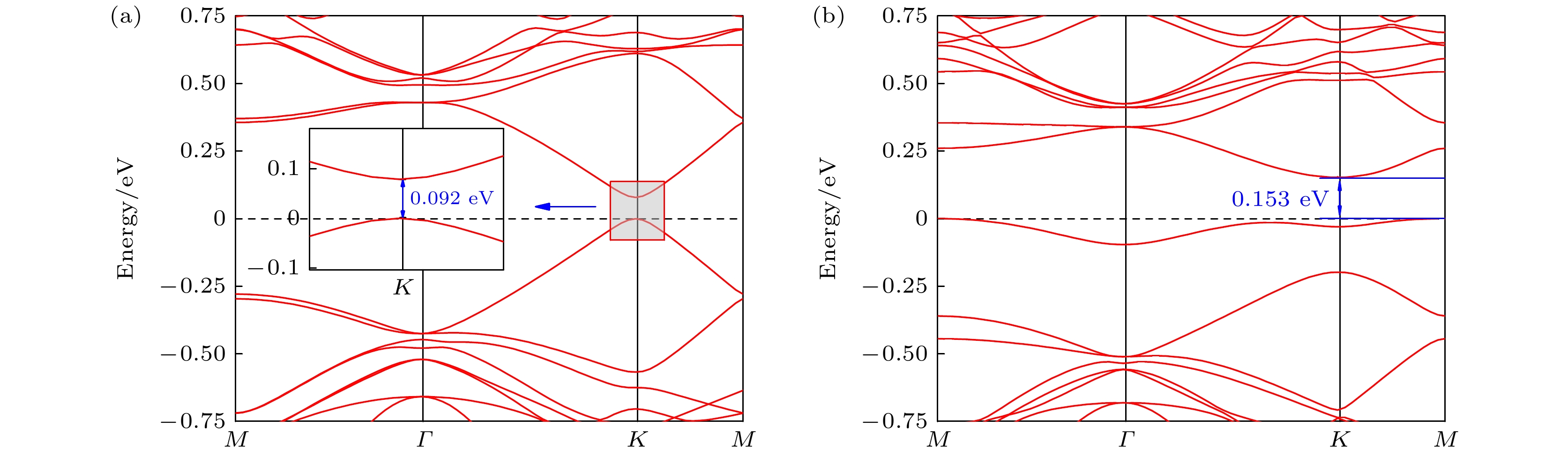
锡烯具有超高载流子密度、无质量狄拉克费米子和高导热性等优良性质, 并且存在能带反转现象, 被认为是拓扑绝缘体, 拓扑绝缘体在一定条件下可以获得无耗散电流, 具有极高的应用潜力. 由于锡烯在布里渊区高对称点K处的能带存在狄拉克锥, 带隙为零, 大大限制了锡烯在半导体领域的应用. 本文采用在锡烯中掺杂B/N元素和在垂直于锡烯平面方向施加电场的方法来打开锡烯在K点处的带隙, 并研究掺杂和施加电场强度对锡烯结构和电子性质的变化. 研究发现施加掺杂B元素和垂直电场都能在保留锡烯拓扑性质的同时打开K点处的带隙, 并且施加的垂直电场强度与K点处带隙呈正相关. 在掺杂B元素的同时施加垂直电场可以增大K点处的带隙, 当电场强度为0.5 V/Å时, 带隙达到0.092 eV. 掺杂N元素后, 锡烯变为间接带隙半导体, 带隙为0.183 eV. 施加垂直电场不能改变N元素掺杂锡烯的结构, 施加的垂直电场强度与K点处带隙则呈负相关, 当电场强度为0.5 V/Å时, K点处带隙减小到0.153 eV.Stanene possesses excellent properties, including an extremely high charge carrier density, massless Dirac fermions, and high thermal conductivity. Moreover, it exhibits band inversion phenomena, being made a candidate for a topological insulator. Topological insulators can generate dissipationless electric currents under certain conditions, showing great application potentials. However, the presence of a Dirac cone in the band structure of stanene at the high-symmetry point K in the Brillouin zone, resulting in a zero band gap, significantly limits its applications in the semiconductor field. This study adopts the method of doping B/N elements in stanene and applying an electric field perpendicular to the stanene to open the band gap at the K point. The effects of doping and the intensity of the applied electric field on the structural and electronic properties of stanene are investigated. The results reveal that both doping B elements and applying a vertical electric field can open the band gap at the K point while preserving the topological properties of stanene. Additionally, there is a positive correlation between the applied vertical electric field intensity and the band gap at the K point. Simultaneously doping B elements and applying a vertical electric field can increase the band gap at the K point, reaching 0.092 eV when the electric field intensity is 0.5 V/Å. After doping N elements, stanene is transformed into an indirect band gap semiconductor with a band gap of 0.183 eV. Applying a vertical electric field cannot change the structure of N-doped stanene, and the intensity of the applied vertical electric field is negatively correlated with the band gap at the K point. When the electric field intensity is 0.5 V/Å, the band gap at the K point decreases to 0.153 eV.
-
Keywords:
- stanene /
- topological insulator /
- perpendicular electric field /
- doping
[1] Luo B, Wang B, Li X L, Jia Y Y, Liang M H, Zhi L J 2012 Adv. Mater. 24 3538
 Google Scholar
[2] Cahangirov S, Topsakal M, Akturk E, Sahin H, Ciraci S 2009 Phys. Rev. Lett. 102 236804
Google Scholar
[3] Roome N J, Carey J D 2014 ACS Appl. Mater. Interfaces 6 7743
Google Scholar
[4] Liu C C, Jiang H, Yao Y G 2011 Phys. Rev. B 84 195430
Google Scholar
[5] Xu Y, Yan B H, Zhang H J, Wang J, Xu G, Tang P Z, Duan W H, Zhang S C 2013 Phys. Rev. Lett. 111 136804
Google Scholar
[6] Zhu F F, Chen W J, Xu Y, Gao C L 2015 Nat. Mater. 14 1020
Google Scholar
[7] Gao J, Zhang G, Zhang Y W 2016 Sci. Rep. 6 29107
Google Scholar
[8] Yuhara J, Fujii Y, Nishino K, Isobe N, Nakatake M, Xian L, Rubio A, Le Lay G 2018 2D Mater. 5 025002
Google Scholar
[9] Deng J J, Xia B Y, Ma X C, Chen H Q, Shan H, Zhai X F, Li B, Zhao A D, Xu Y, Duan W H, Zhang S C, Wang B, Hou J G 2018 Nat. Mater. 17 1081
Google Scholar
[10] 郑晓虎, 张建峰, 杜瑞瑞 2022 物理学报 71 186401
Google Scholar
Zheng X H, Zhang J F, Du R R 2022 Acta Phys. Sin. 71 186401
Google Scholar
[11] 钱冬, 贾金锋 2016 科学通报 61 3252
Qian D, Jia J F 2016 Chin. Sci. Bul. 61 3252
[12] Wu S C, Shan G, Yan B H 2014 Phys. Rev. Lett. 113 256401
Google Scholar
[13] Qi X L, Zhang S C 2011 Rev. Mod. Phys. 83 1057
Google Scholar
[14] Ren C C, Ji W X, Zhang C W, Li P, Wang P J 2016 Mater. Res. Express 3 105008
Google Scholar
[15] Garg P, Choudhuri I, Mahata A, Pathak B 2017 Phys. Chem. Chem. Phys. 19 3660
Google Scholar
[16] Pribram Jones A, Pittalis S, Gross E, Burke K Frontiers and Challenges in Warm Dense Matter (Cham, Switzerland: Springer) pp25–60
[17] Perdew J P, Burke K, Ernzerhof M 1996 Phys. Rev. Lett. 77 3865
Google Scholar
[18] Perdew J P, Chevary J A, Vosko S H, Jackson K A, Pederson M R, Singh D J, Fiolhais C 1992 Phys. Rev. B 46 6671
Google Scholar
[19] Hamann D R 2013 Phys. Rev. B 88 085117
Google Scholar
[20] Monkhorst H J, Pack J D 1976 Phys. Rev. B 13 5188
Google Scholar
[21] Liu D C, Nocedal J 1989 Math. Program 45 503
Google Scholar
[22] Hänggi P, Thomas H 1982 Phy. Rep. 88 207
Google Scholar
[23] Xing D X, Ren C C, Zhang S F, Feng Y, Chen X L, Zhang C W, Wang P J 2017 Superlattices Microstruct. 103 139
Google Scholar
[24] Dai X Q, Zhao M Y, Zhao R M, Li W 2017 Superlattices Microstruct. 106 33
Google Scholar
[25] Zhao C X, Jia J F 2020 Front. Phys. 15 53201
Google Scholar
[26] Fu L, Kane C L 2007 Phys. Rev. B 76 045302
Google Scholar
[27] Nika D, Pokatilov E, Askerov A, Balandin A A 2009 Phys. Rev. B 79 155413
Google Scholar
[28] Baroni S, de Gironcoli S, Dal Corso A, Giannozzi P 2001 Rev. Mod. Phys. 73 515
Google Scholar
[29] Van den Broek B, Houssa M, Scalise E, Pourtois G, Afanas'ev V V, Stesmans A 2014 2D Mater. 1 021004
Google Scholar
[30] Zhou J, Huang J, Sumpter B G, Kent P R C, Xie Y, Terrones H, Smith S C 2014 J. Phys. Chem. C 118 16236
Google Scholar
[31] Zhang Z, Liu X, Yakobson B I, Guo W 2012 J. Am. Chem. Soc. 134 19326
Google Scholar
-

图 1 锡烯优化后的结构图, 上方是锡烯结构主视图, 下方是锡烯结构的侧视图, 其中θ为锡烯键角, a和b为锡烯晶格常数, l为Sn—Sn键长, E为外加电场, d为锡烯的屈曲
Fig. 1. Optimized structure of stanene and doped stanene. The top part is the top view of the structure of stanene, the bottom part is side view of the structure of stanene, where θ represents the bond angle of stanene, a and b represent the lattice constants of stanene, l represents the Sn—Sn bond length, E represents electric field, d represents the buckling of stanene.
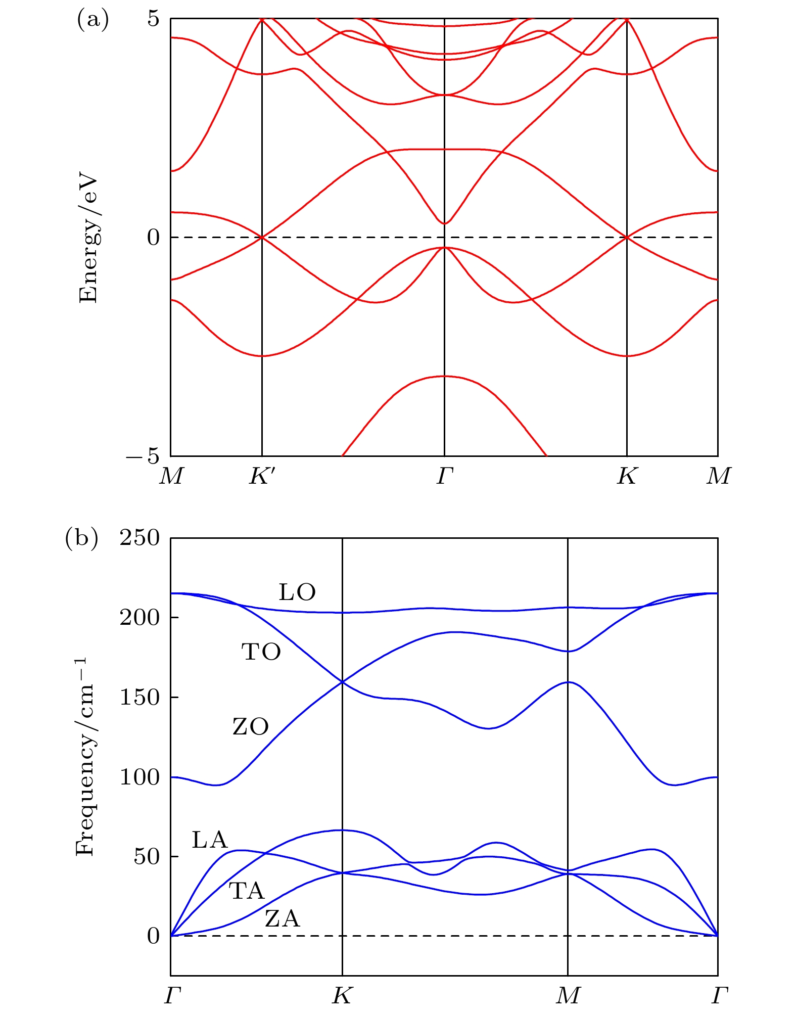
图 2 (a) 锡烯的能带图, 费米能级设在0 eV处; (b) 无应力锡烯的声子谱, 从下到上依次为ZA, TA, LA, ZO, TO和 LO
Fig. 2. (a) Band structure of stanene, the Fermi level is set to zero; (b) phonon spectrum of stress-free stanene, which are ZA (acoustic out-of-plane mode), TA (acoustic in-plane transverse mode), LA (acoustic in-plane longitudinal mode), ZO (optical out-of-plane mode), TO (optical in-plane transverse mode), LO (optical in-plane longitudinal mode), respectively from bottom to top.

图 3 (a) 电场强度为0—0.5 V/Å时锡烯晶格常数、Sn—Sn键长和屈曲的变化; (b) 电场强度为0.5 V/Å时锡烯的能带图; (c) 电场强度为0—0.5 V/Å时锡烯在K点处的带隙, 费米能级设在0 eV处
Fig. 3. (a) The change of lattice constant, Sn—Sn bond length, and buckling of stanene under the electric field ranging from 0 to 0.5 V/Å; (b) the band gap of stanene under the electric field of 0.5 V/Å; (c) the band gap at the K point of stanene under the electric field ranging from 0 to 0.5 V/Å. The Fermi level is set to zero.

图 4 (a) B掺杂锡烯优化后的结构图, 上方是B掺杂锡烯结构主视图, 下方是B掺杂锡烯结构的侧视图; (b) B掺杂锡烯的差分电荷密度图; (c) B掺杂锡烯的能带图; (d) B掺杂锡烯的声子色散图
Fig. 4. (a) Optimized structure of B-doped stanene, the top part is the top view of the structure of B-doped stanene, the bottom part is side view of the structure of B-doped stanene; (b) electron density difference of B-doped stanene; (c) energy band of B-doped stanene; (d) phonon spectrum of stress-free B-doped stanene.
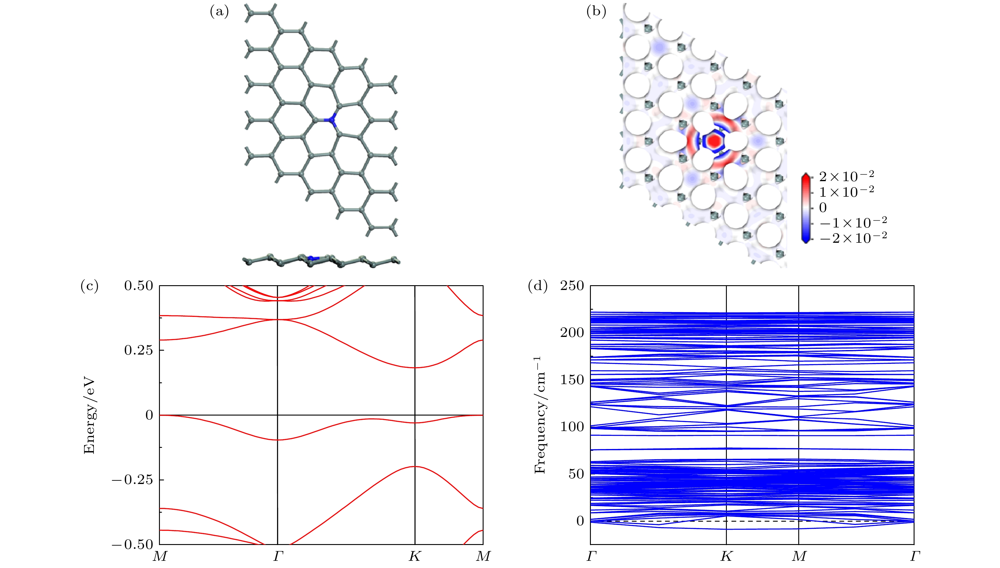
图 5 (a) N掺杂锡烯优化后的结构图, 上方是N掺杂锡烯结构主视图, 下方是N掺杂锡烯结构的侧视图; (b) N掺杂锡烯的差分电荷密度图; (c) N掺杂锡烯的能带图; (d) N掺杂锡烯的声子色散图
Fig. 5. (a) Optimized structure of N-doped stanene, the top part is the top view of the structure of N-doped stanene, the bottom part is side view of the structure of N-doped stanene; (b) electron density difference of N-doped stanene; (c) energy band of N-doped stanene; (d) phonon spectrum of stress-free N-doped stanene.
-
[1] Luo B, Wang B, Li X L, Jia Y Y, Liang M H, Zhi L J 2012 Adv. Mater. 24 3538
Google Scholar
[2] Cahangirov S, Topsakal M, Akturk E, Sahin H, Ciraci S 2009 Phys. Rev. Lett. 102 236804
Google Scholar
[3] Roome N J, Carey J D 2014 ACS Appl. Mater. Interfaces 6 7743
Google Scholar
[4] Liu C C, Jiang H, Yao Y G 2011 Phys. Rev. B 84 195430
Google Scholar
[5] Xu Y, Yan B H, Zhang H J, Wang J, Xu G, Tang P Z, Duan W H, Zhang S C 2013 Phys. Rev. Lett. 111 136804
Google Scholar
[6] Zhu F F, Chen W J, Xu Y, Gao C L 2015 Nat. Mater. 14 1020
Google Scholar
[7] Gao J, Zhang G, Zhang Y W 2016 Sci. Rep. 6 29107
Google Scholar
[8] Yuhara J, Fujii Y, Nishino K, Isobe N, Nakatake M, Xian L, Rubio A, Le Lay G 2018 2D Mater. 5 025002
Google Scholar
[9] Deng J J, Xia B Y, Ma X C, Chen H Q, Shan H, Zhai X F, Li B, Zhao A D, Xu Y, Duan W H, Zhang S C, Wang B, Hou J G 2018 Nat. Mater. 17 1081
Google Scholar
[10] 郑晓虎, 张建峰, 杜瑞瑞 2022 物理学报 71 186401
Google Scholar
Zheng X H, Zhang J F, Du R R 2022 Acta Phys. Sin. 71 186401
Google Scholar
[11] 钱冬, 贾金锋 2016 科学通报 61 3252
Qian D, Jia J F 2016 Chin. Sci. Bul. 61 3252
[12] Wu S C, Shan G, Yan B H 2014 Phys. Rev. Lett. 113 256401
Google Scholar
[13] Qi X L, Zhang S C 2011 Rev. Mod. Phys. 83 1057
Google Scholar
[14] Ren C C, Ji W X, Zhang C W, Li P, Wang P J 2016 Mater. Res. Express 3 105008
Google Scholar
[15] Garg P, Choudhuri I, Mahata A, Pathak B 2017 Phys. Chem. Chem. Phys. 19 3660
Google Scholar
[16] Pribram Jones A, Pittalis S, Gross E, Burke K Frontiers and Challenges in Warm Dense Matter (Cham, Switzerland: Springer) pp25–60
[17] Perdew J P, Burke K, Ernzerhof M 1996 Phys. Rev. Lett. 77 3865
Google Scholar
[18] Perdew J P, Chevary J A, Vosko S H, Jackson K A, Pederson M R, Singh D J, Fiolhais C 1992 Phys. Rev. B 46 6671
Google Scholar
[19] Hamann D R 2013 Phys. Rev. B 88 085117
Google Scholar
[20] Monkhorst H J, Pack J D 1976 Phys. Rev. B 13 5188
Google Scholar
[21] Liu D C, Nocedal J 1989 Math. Program 45 503
Google Scholar
[22] Hänggi P, Thomas H 1982 Phy. Rep. 88 207
Google Scholar
[23] Xing D X, Ren C C, Zhang S F, Feng Y, Chen X L, Zhang C W, Wang P J 2017 Superlattices Microstruct. 103 139
Google Scholar
[24] Dai X Q, Zhao M Y, Zhao R M, Li W 2017 Superlattices Microstruct. 106 33
Google Scholar
[25] Zhao C X, Jia J F 2020 Front. Phys. 15 53201
Google Scholar
[26] Fu L, Kane C L 2007 Phys. Rev. B 76 045302
Google Scholar
[27] Nika D, Pokatilov E, Askerov A, Balandin A A 2009 Phys. Rev. B 79 155413
Google Scholar
[28] Baroni S, de Gironcoli S, Dal Corso A, Giannozzi P 2001 Rev. Mod. Phys. 73 515
Google Scholar
[29] Van den Broek B, Houssa M, Scalise E, Pourtois G, Afanas'ev V V, Stesmans A 2014 2D Mater. 1 021004
Google Scholar
[30] Zhou J, Huang J, Sumpter B G, Kent P R C, Xie Y, Terrones H, Smith S C 2014 J. Phys. Chem. C 118 16236
Google Scholar
[31] Zhang Z, Liu X, Yakobson B I, Guo W 2012 J. Am. Chem. Soc. 134 19326
Google Scholar

 下载:
下载:
计量
- 文章访问数: 319
- PDF下载量: 9
- 被引次数: 0
