


-
Void embedded silicon-on-insulator (VESOI) substrate is a newly developed silicon-on-insulator (SOI) substrate for advanced complementary metal oxide semiconductor (CMOS) devices and integration technology. However, in the ion-cutting process for preparing the substrate, numerous hydrogen bubbles aggregate at the cut interface, which compresses the cavity structure and might cause the thin film above the cavity to be damaged and delaminated. Therefore, it is necessary to conduct in-depth research on the stress mechanism and process stability in the preparation of VESOI substrates. This study focuses on a single rectangular cavity structure and uses the fixed-supported beam theory to analyze its mechanical behavior during fabrication, and a three-dimensional model of cavity structure is constructed by using the finite element analysis tool. Through stress simulation, the failure mechanism of the cavity structure is identified, and the weak points are confirmed. The results show that the short side length (w), top silicon film thickness (t), and hydrogen bubble pressure are the main factors affecting the stress state of the top silicon film. When the w/t ratio exceeds 4–5, the silicon film will fracture owing to excessive tensile stress, and the fracture site is along the long side of the rectangular cavity. By increasing the thickness of the top silicon film slightly and adding support structures inside the cavity (to reduce w), this work successfully prepares high-quality 8-inch VESOI substrates that meet the requirements for the CMOS production line. The present study is expected to provide valuable idea for the development of integrated technologies relying on VESOI substrates.
-
Keywords:
- void embedded silicon-on-insulator /
- ion cutting /
- stress /
- finite element stress simulation
[1] 王阳元 2018 集成电路产业全书(下卷) (北京: 电子工业出版社) 第1543—1562页
Wang Y Y 2018 Integrated Circuit Industry (Vol. 2) (Beijing: Electronic Industry Press) pp1543–1562 (in Chinese)
[2] Kononchuk O, Nguyen B Y 2014 Silicon-on-Insulator (SOI) Technology: Manufacture and Applications (Britain: Woodhead Publishing) pp395–435
[3] Liu Q, Mu Z Q, Liua C H, Zhao L T, Yu W J 2021 IEEE Electron Dev. Lett. 42 657
 Google Scholar
[4] 金成吉, 张苗苗, 李开轩, 刘宁, 玉虓, 韩根全 2021 微纳电子与智能制造 3 32
Jin C J, Zhang M M, Li K X, Liu N, Yu X, Han G Q 2021 Micro/Nano Electron. Intell. Manuf. 3 32
[5] 张彦伟 2014 硕士学位论文 (湖南: 湘潭大学)
Zhang Y Y 2014 M. S. Thesis (Hunan: Xiangtan University) (in Chinese)
[6] 贺琪, 顾祥, 纪旭明, 李金航, 赵晓松 2020 微处理机 41 41
Google Scholar
He Q, Gu X, Ji X M, Li J H, Zhao X S 2020 Microprocessors 41 41
Google Scholar
[7] 林青 2004 博士学位论文 (上海: 中国科学院上海微系统与信息技术研究所)
Lin Q 2004 Ph. D. Dissertation (Shanghai: Shanghai Institute of Microsystem and Information Technology) (in Chinese)
[8] Nguyen B Y, Celler G, Mazuré C 2009 JICS 4 51
Google Scholar
[9] Palkuti L, Alles M, Hughes H 2014 SOI-3D-Subthreshold Microelectronics Technology Unified Conference (S3S) Millbrae, CA, USA, October 6–9 2014 p1
[10] Qing D Z, Jian W W, Jin H L, Shuai S, Xu M J, Xiang G, Gen S H, Bing L 2021 At. Energy Sci. Technol. 55 2151
[11] 古美良 胡明 2006 压电与声光 28 236
Gu M L, Hu M 2006 Piezoelectr. Acoustoopt. 28 236
[12] 林成鲁 2003 半导体技术 9 39
Google Scholar
Lin C L 2003 Semicond. Technol. 9 39
Google Scholar
[13] 刘强 2021 博士学位论文 (上海: 中国科学院上海微系统与信息技术研究所)
Lin Q 2021 Ph. D. Dissertation (Shanghai: Shanghai Institute of Microsystem and Information Technology) (in Chinese)
[14] Liu Q, Zhou H Y, Jia X, Yang Y M, Mu Z Q, Wei X, Yu W J 2022 IEEE Electron Dev. Lett. 43 1814
Google Scholar
[15] Zhao L T, Liu Q, Liu C H, Chen L L, Yang Y M, Wei X, Mu Z Q, Yu W J 2021 IEEE Electron Dev. Lett. 42 1428
Google Scholar
[16] 刘恩科, 朱秉升, 罗晋生 2008 半导体物理学(第7版) (北京: 电子工业出版社) 第204—235页
Liu E K, Zhu B S, Luo J S 2008 Semiconductor Physics (7th Ed.) (Beijing: Publishing House of Electronics Industry) pp204–235 (in Chinese)
[17] Roundy D, Cohen M L 2001 Phys. Rev. B 64 212103
[18] Dubois M M, Rignanese G M, Pardoen T, Charlier J C 2006 Phys. Rev. B 74 235203
Google Scholar
[19] Umeno Y, Kushima A, Kitamura T, Gumbsch P, Li J 2005 Phys. Rev. B 72 165431
Google Scholar
[20] Moriceau H, Mazen F, Braley C, Rieutord F, Tauzin A, Deguet C 2012 Nucl. Instrum. Methods Phys. Res. 277 84
Google Scholar
[21] Daval N, Schwarzenbach W, Moulin C, Bonnin O, Maleville C 2013 VLSI Technology, Systems, and Applications (VLSI-TSA), 2013 International Symposium Hsinchu, Taiwan, China, April 22–24, 2013 p1
[22] Wang B, Gu B, Zhang H, Feng X 2016 Acta Mech. Solida Sin. 29 111
Google Scholar
[23] Lagahe-Blanchard C, Sousbie N, Sartori S, Moriceau H, Blondeau B 2003 Proc. Electrochem. Soc. 19 346
[24] Hchbauer T 2001 Ph. D. Dissertation (Germany: University of Marburg)
[25] Radu I 2022 Ph. D. Dissertation (Germany: Martin-Luther-Universität Halle-Wittenberg)
[26] Yun C H, Cheung N W 2000 J. Microelectromech. Syst. 9 474
Google Scholar
[27] 范钦珊, 殷雅俊, 唐靖林 2014 材料力学 (第3版) (北京: 清华大学出版社) 第126—204页
Fan Q S, Yin Y J, Tang J L 2014 Material Mechanics (3rd Ed.) (Beijing: Tsinghua University Press) pp126–204 (in Chinese)
[28] Craig Jr R R, Taleff E M 2020 Mechanics of Materials (State of New Jersey: John Wiley & Sons) pp286–293
[29] Franssila S 2005 Introduction to Microfabrication (England: Wiley publication) pp174–182
[30] Schmidt B, Wetzig K 2012 Ion Beams in Materials Processing and Analysis (Vienna: Springer) pp117–235
[31] Nguyen P, Cayrefourcq I, Bourdelle K K, Boussagol A, Guiot E, Mohamed N B, Sousbie N, Akatsu T 2005 J. Appl. Phys. 97 083527
-

图 1 (a) VESOI衬底制备工艺流程; (b)基于VESOI衬底可构造的10种内嵌空腔结构
Figure 1. (a) Fabrication process of VESOI substrate; (b) ten types of embedded void structures based on VESOI substrates.

图 2 (a)基于VESOI衬底可制备无背栅SOI器件和GAA器件; (b)无背栅SOI器件和VESOI GAA器件的转移特性曲线; (c)两种器件的亚阈值斜率随漏极电流变化情况
Figure 2. (a) Backgate-free SOI and GAA devices based on VESOI substrates; (b) transfer characteristics of backgate-free SOI and GAA devices; (c) subthreshold swing vs. drain current for backgate-free SOI and GAA devices.

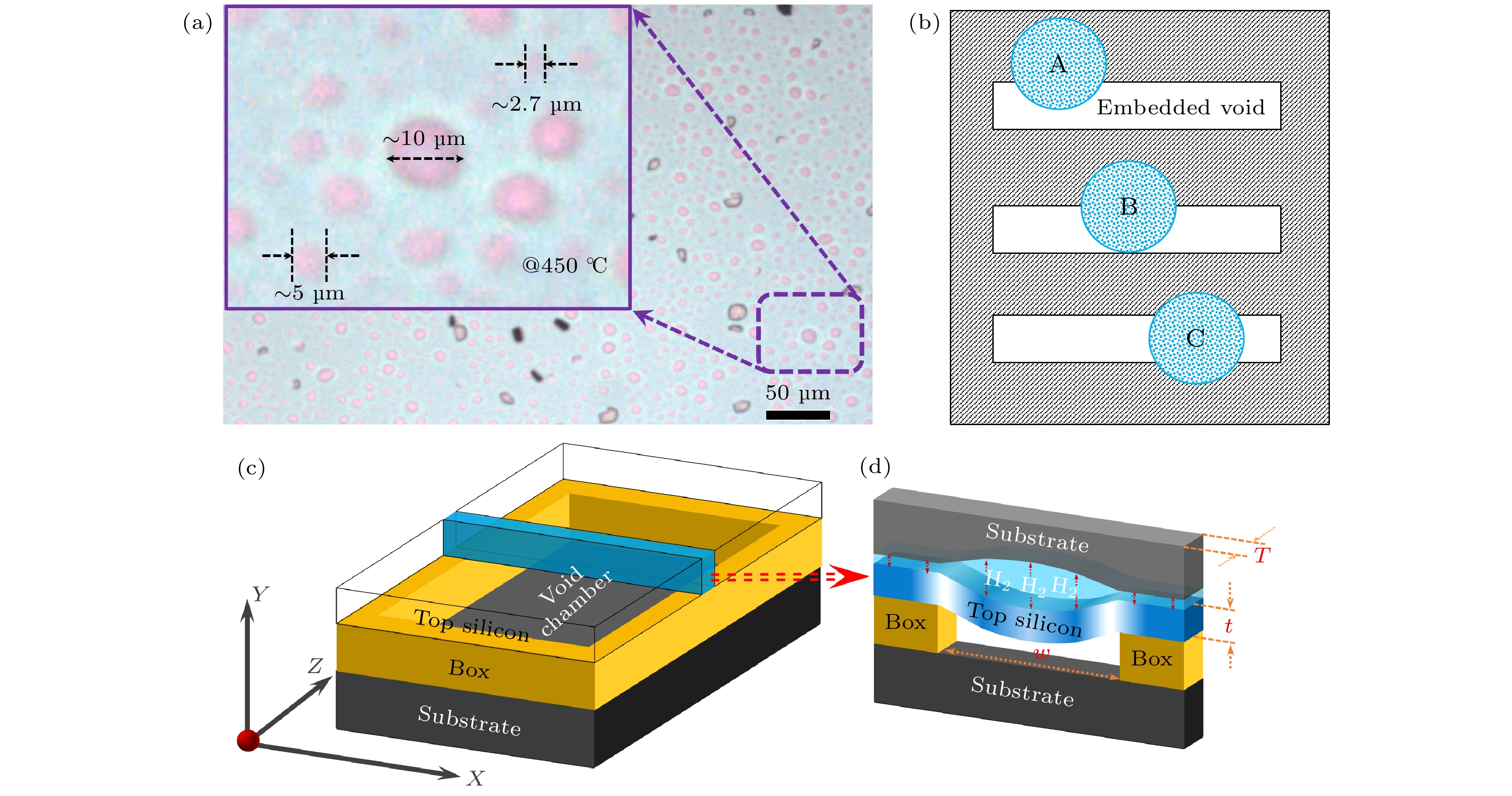
图 4 (a)离子剥离试验中硅衬底表面的氢气泡剥离现象; (b)氢气泡与内嵌空腔可能存在的位置关系; (c), (d)简化的顶层硅受力示意图
Figure 4. (a) Hydrogen blistering phenomenon on the silicon substrate surface during ion-cutting experiment; (b) possible positions of the hydrogen blister with respect to the embedded void structure; (c), (d) simplified schematic of splitting force on top silicon.

图 5 (a), (b)简支梁受力模型及其弯矩分布图; (c), (d)固支梁受力模型及其弯矩分布图
Figure 5. (a), (b) Schematic diagram of simply supported beam structure and the related bending moment distribution curve; (c), (d) schematic diagram of fixed beam structure and the related bending moment distribution curve.
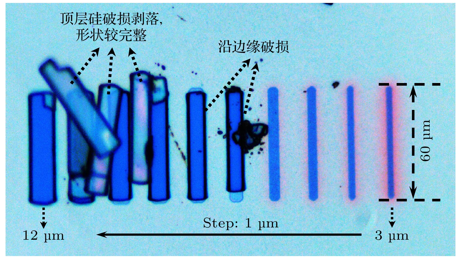
图 6 空腔宽度变化对空腔结构破损行为的影响
Figure 6. Effect of variations in chamber width on the breakage behavior of embedded void structure.
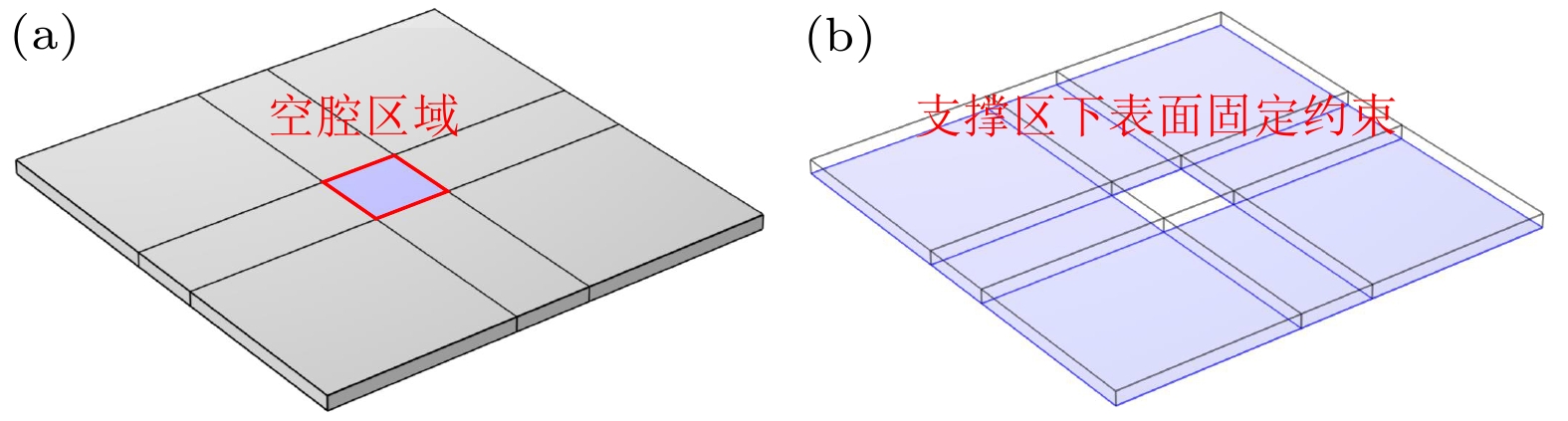
图 7 (a)空腔结构几何模型(空腔区域); (b)空腔结构几何模型(固定约束区域)
Figure 7. (a) Geometric model of VESOI void structure (the area of chambers); (b) geometric model of VESOI void structure (the area of fixed constraint).

图 8 正方形空腔和长方形空腔在均布载荷下的有限元应力仿真
Figure 8. Finite element stress simulation of square and rectangular voids under uniformly distributed load.

图 9 顶硅薄膜上表面与下表面最大应力大小随空腔宽度w和薄膜厚度t的变化趋势 (a) t = 0.1 μm; (b) t = 0.25 μm; (c) t = 1 μm
Figure 9. Variation trend of the maximum stress magnitude on top/bottom surfaces of top silicon with different chamber widths and the top silicon thicknesses: (a) t = 0.1 μm; (b) t = 0.25 μm; (c) t = 1 μm.

图 10 空腔上方顶层硅的上下表面第一主应力随空腔宽度
$ w $ 的变化趋势(L表示矩形空腔一边的长度) (a) L = 4, w = 0.8 μm; (b) L = 4 μm, w = 1.2 μm; (c) L = 4 μm, w = 2.1 μmFigure 10. Trend of the first principal stress on the top/bottom surfaces of the top silicon layer with respect to the chamber width
$ w $ : (a) L = 4 μm, w = 0.8 μm; (b) L = 4 μm, w = 1.2 μm; (c) L = 4 μm, w = 2.1 μm.
图 11 空腔上方顶层硅应力极值随空腔结构参数变化的趋势
Figure 11. Stress level of top silicon layer with different thicknesses and chamber widths.
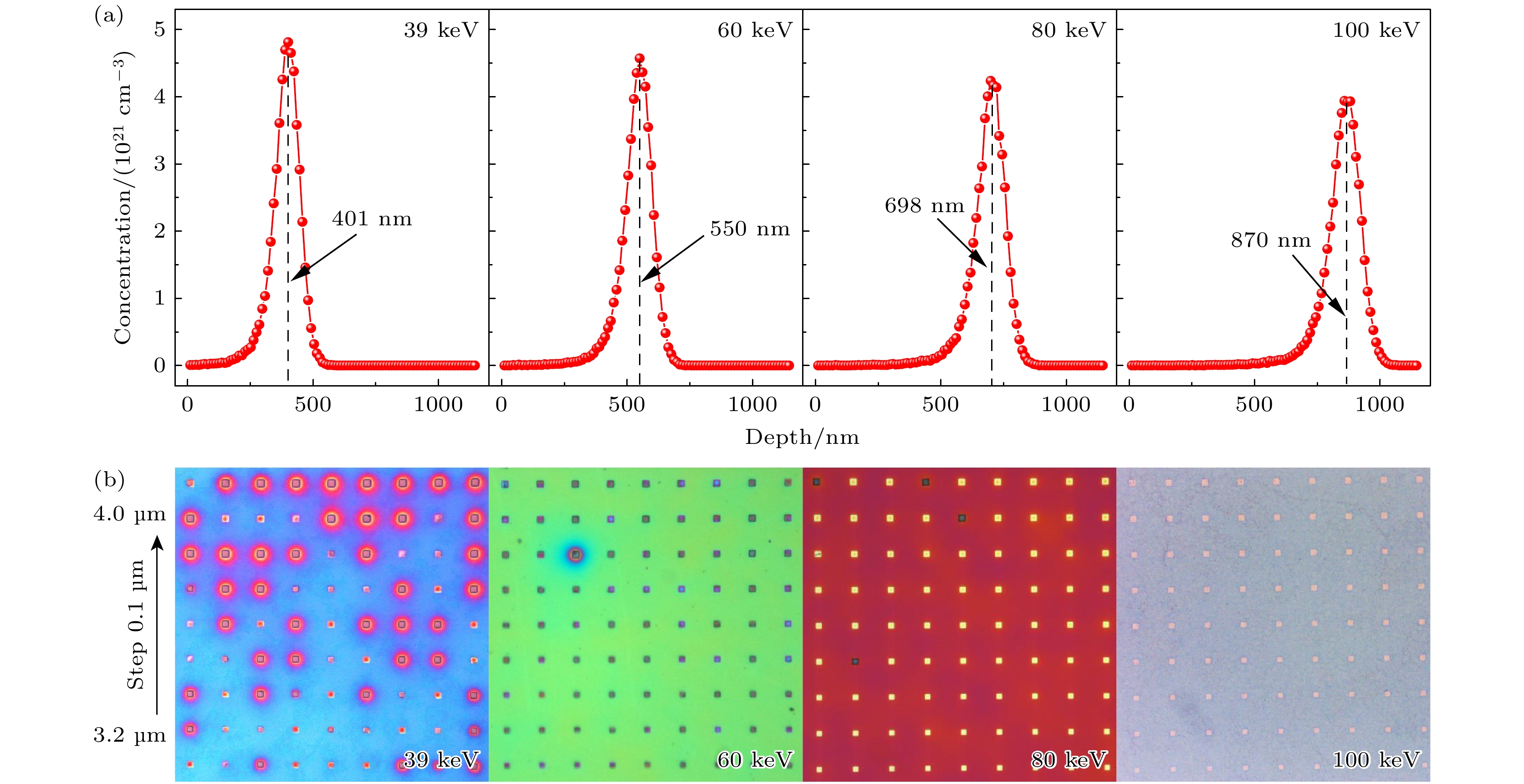
图 12 剥离厚度对空腔上方顶层硅破损行为的影响 (a)不同氢离子注入能量下的顶层硅剥离厚度; (b)不同剥离厚度下的顶层硅破损情况
Figure 12. Influence of ion-cutting thickness on the top silicon breakage behavior: (a) Relationship between top silicon thickness and hydrogen ion implantation energy; (b) impact of different peel thicknesses on the top silicon layer damage.

图 13 内嵌空腔结构对空腔上方顶层硅应力分布状态的影响 (a)正方形空腔; (b) 带支撑结构的正方形空腔; (c) 圆形空腔; (d)带支撑结构的圆形空腔
Figure 13. Impact of chamber structures on the stress distribution within top silicon: (a) Square chamber configuration; (b) square chamber configuration with an additional support pillar; (c) circular chamber configuration; (d) circular chamber configuration with an additional support pillar.

图 14 (a) 8 in高质量VESOI衬底; (b)内含支撑柱结构, 边长为54.5 μm的正方形内嵌空腔; (c)面向高密度集成的密排内嵌空腔阵列
Figure 14. (a) High quality 8-in VESOI substrate; (b) the scanning electron microscope image of a square embedded void with 54.5 μm side length, where supporting pillars were set inside the chamber; (c) dense array of embedded void chambers for possible high-density integration.
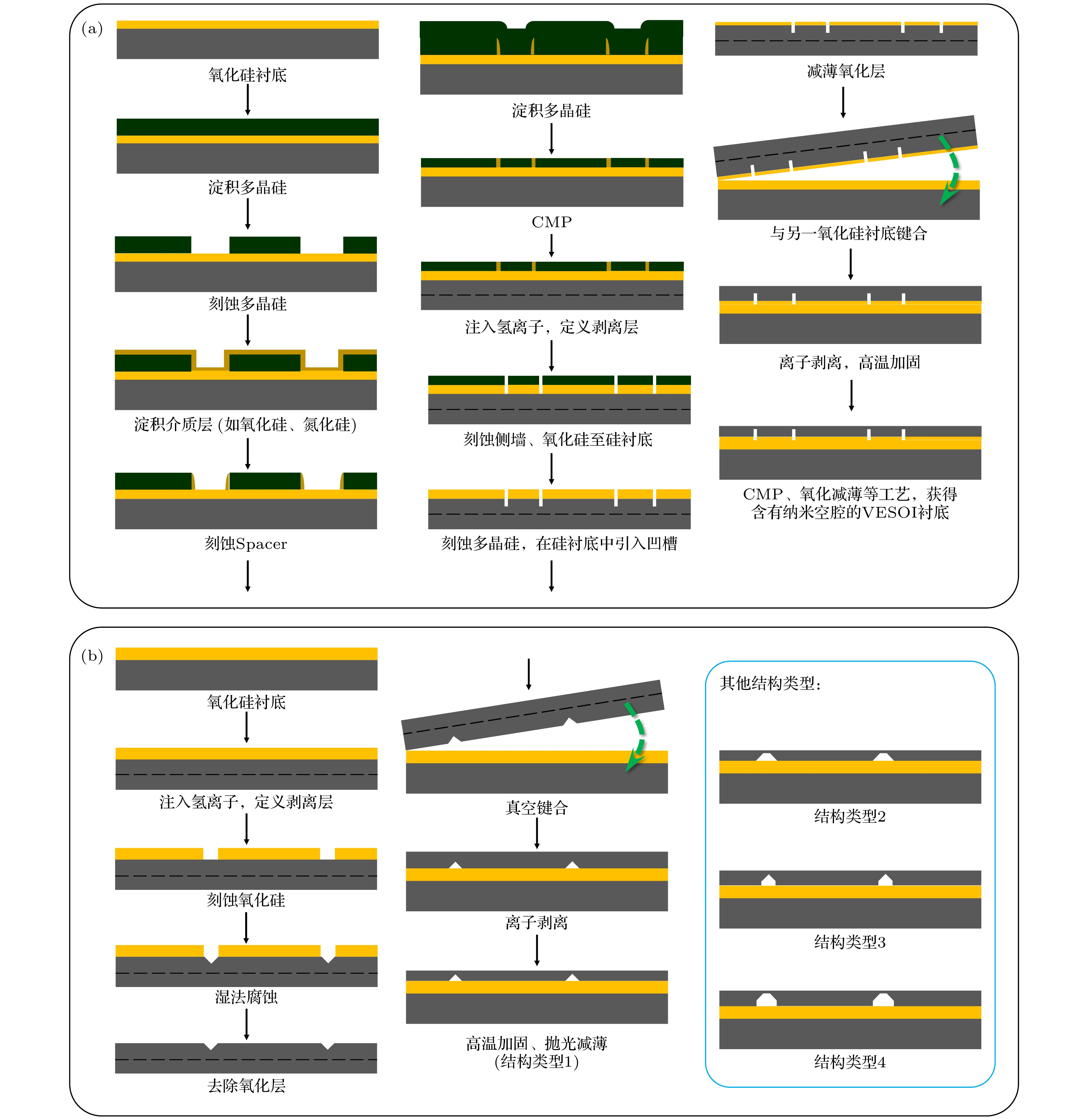
图 15 (a) Spacer掩膜法制备纳米级空腔型VESOI衬底; (b)各向异性湿法腐蚀制备纳米级空腔型VESOI衬底
Figure 15. (a) Fabrication of VESOI substrate with nano-meter voids using spacer pattern; (b) the fabrication of VESOI substrate with nano-meter voids using anisotropic wet etching method.
表 1 空腔结构几何模型材料与结构参数
Table 1. Geometric and materials’ parameters of the VESOI void structure.
参数名称 数值 空腔宽度 w/μm 参数化扫描(0.1—10, 步长0.3) 空腔长度 L/μm 10, 4 顶层硅厚度 t/μm 参数化扫描(0.1—1, 步长0.1) 杨氏模量E/GPa 170 泊松比 ν 0.28 密度$ \rho $/(kg·m–3) 2329  DownLoad: CSV
-
[1] 王阳元 2018 集成电路产业全书(下卷) (北京: 电子工业出版社) 第1543—1562页
Wang Y Y 2018 Integrated Circuit Industry (Vol. 2) (Beijing: Electronic Industry Press) pp1543–1562 (in Chinese)
[2] Kononchuk O, Nguyen B Y 2014 Silicon-on-Insulator (SOI) Technology: Manufacture and Applications (Britain: Woodhead Publishing) pp395–435
[3] Liu Q, Mu Z Q, Liua C H, Zhao L T, Yu W J 2021 IEEE Electron Dev. Lett. 42 657
Google Scholar
[4] 金成吉, 张苗苗, 李开轩, 刘宁, 玉虓, 韩根全 2021 微纳电子与智能制造 3 32
Jin C J, Zhang M M, Li K X, Liu N, Yu X, Han G Q 2021 Micro/Nano Electron. Intell. Manuf. 3 32
[5] 张彦伟 2014 硕士学位论文 (湖南: 湘潭大学)
Zhang Y Y 2014 M. S. Thesis (Hunan: Xiangtan University) (in Chinese)
[6] 贺琪, 顾祥, 纪旭明, 李金航, 赵晓松 2020 微处理机 41 41
Google Scholar
He Q, Gu X, Ji X M, Li J H, Zhao X S 2020 Microprocessors 41 41
Google Scholar
[7] 林青 2004 博士学位论文 (上海: 中国科学院上海微系统与信息技术研究所)
Lin Q 2004 Ph. D. Dissertation (Shanghai: Shanghai Institute of Microsystem and Information Technology) (in Chinese)
[8] Nguyen B Y, Celler G, Mazuré C 2009 JICS 4 51
Google Scholar
[9] Palkuti L, Alles M, Hughes H 2014 SOI-3D-Subthreshold Microelectronics Technology Unified Conference (S3S) Millbrae, CA, USA, October 6–9 2014 p1
[10] Qing D Z, Jian W W, Jin H L, Shuai S, Xu M J, Xiang G, Gen S H, Bing L 2021 At. Energy Sci. Technol. 55 2151
[11] 古美良 胡明 2006 压电与声光 28 236
Gu M L, Hu M 2006 Piezoelectr. Acoustoopt. 28 236
[12] 林成鲁 2003 半导体技术 9 39
Google Scholar
Lin C L 2003 Semicond. Technol. 9 39
Google Scholar
[13] 刘强 2021 博士学位论文 (上海: 中国科学院上海微系统与信息技术研究所)
Lin Q 2021 Ph. D. Dissertation (Shanghai: Shanghai Institute of Microsystem and Information Technology) (in Chinese)
[14] Liu Q, Zhou H Y, Jia X, Yang Y M, Mu Z Q, Wei X, Yu W J 2022 IEEE Electron Dev. Lett. 43 1814
Google Scholar
[15] Zhao L T, Liu Q, Liu C H, Chen L L, Yang Y M, Wei X, Mu Z Q, Yu W J 2021 IEEE Electron Dev. Lett. 42 1428
Google Scholar
[16] 刘恩科, 朱秉升, 罗晋生 2008 半导体物理学(第7版) (北京: 电子工业出版社) 第204—235页
Liu E K, Zhu B S, Luo J S 2008 Semiconductor Physics (7th Ed.) (Beijing: Publishing House of Electronics Industry) pp204–235 (in Chinese)
[17] Roundy D, Cohen M L 2001 Phys. Rev. B 64 212103
[18] Dubois M M, Rignanese G M, Pardoen T, Charlier J C 2006 Phys. Rev. B 74 235203
Google Scholar
[19] Umeno Y, Kushima A, Kitamura T, Gumbsch P, Li J 2005 Phys. Rev. B 72 165431
Google Scholar
[20] Moriceau H, Mazen F, Braley C, Rieutord F, Tauzin A, Deguet C 2012 Nucl. Instrum. Methods Phys. Res. 277 84
Google Scholar
[21] Daval N, Schwarzenbach W, Moulin C, Bonnin O, Maleville C 2013 VLSI Technology, Systems, and Applications (VLSI-TSA), 2013 International Symposium Hsinchu, Taiwan, China, April 22–24, 2013 p1
[22] Wang B, Gu B, Zhang H, Feng X 2016 Acta Mech. Solida Sin. 29 111
Google Scholar
[23] Lagahe-Blanchard C, Sousbie N, Sartori S, Moriceau H, Blondeau B 2003 Proc. Electrochem. Soc. 19 346
[24] Hchbauer T 2001 Ph. D. Dissertation (Germany: University of Marburg)
[25] Radu I 2022 Ph. D. Dissertation (Germany: Martin-Luther-Universität Halle-Wittenberg)
[26] Yun C H, Cheung N W 2000 J. Microelectromech. Syst. 9 474
Google Scholar
[27] 范钦珊, 殷雅俊, 唐靖林 2014 材料力学 (第3版) (北京: 清华大学出版社) 第126—204页
Fan Q S, Yin Y J, Tang J L 2014 Material Mechanics (3rd Ed.) (Beijing: Tsinghua University Press) pp126–204 (in Chinese)
[28] Craig Jr R R, Taleff E M 2020 Mechanics of Materials (State of New Jersey: John Wiley & Sons) pp286–293
[29] Franssila S 2005 Introduction to Microfabrication (England: Wiley publication) pp174–182
[30] Schmidt B, Wetzig K 2012 Ion Beams in Materials Processing and Analysis (Vienna: Springer) pp117–235
[31] Nguyen P, Cayrefourcq I, Bourdelle K K, Boussagol A, Guiot E, Mohamed N B, Sousbie N, Akatsu T 2005 J. Appl. Phys. 97 083527

 DownLoad:


Catalog
Metrics
- Abstract views: 2131
- PDF Downloads: 50
- Cited By: 0
