


-
Inkjet printing as a contact-free, high material utilization, low cost, patternable solution processing technology, may become the future color quantum-dot light-emitting diodes (QLED) production of the key technology. However, owing to the existence of the pixel structure of the substrate array, the film prepared by inkjet printing technology is not so smooth and uniform as that by spin coating technology, which affects the luminescence performance of the device. Therefore, it is necessary to study the film forming mechanism and process of inkjet printing. In order to solve the above problems, this paper focuses on the material and process problems of preparing high-quality electronic transport layer ZnO thin films by inkjet printing. From the perspective of ligand, the ZnO quantum dot material, which is an indispensable electron transport layer, is optimized to prepare the thin films with good morphology and stability in air, and the methods to improve the performances of inkjet printing QLED devices are explored. Firstly, the drying process and influence mechanism of ZnO quantum dot ink in air are investigated. As the thickness of ZnO quantum dot film prepared by inkjet printing increases, the film becomes loose and the surface becomes rough with the continuous extension of the time in the air. These changes make the efficiency of the QLED device decrease and the luminous region uneven. The reason for this phenomenon is that after the ZnO quantum dots are printed into the pixel pit, the random Brownian motion of quantum dots will continue in the process of solvent evaporation. In this process, the ligand ethanolamine connected to the surface of ZnO quantum dots will fall off with the movement and cannot play the role in dispersing the quantum dots. Besides, the external water oxygen and carbon dioxide attach to the film. The combination between the two effects makes the ZnO quantum dots aggregate into large particles and the film becomes loose and porous. In this paper, we use ethylenediamine tetraacetic acid (EDTA) as ligand to synthesize ZnO quantum dots, which can effectively improve this phenomenon. The carboxyl group at the end of EDTA is more stable in connection with ZnO quantum dots. Moreover, the EDTA has multiple branch chains, which makes it have steric hindrance effect and can disperse ZnO effectively. A smooth and compact film with a roughness of 1.97 nm is prepared by inkjet printing. After 40 min exposure to air, the film is still able to maintain a stable morphology. Then, based on the EDTA-ZnO quantum dots synthesized above, red QLED devices with optimized performance are prepared. The current efficiency of the spin-coating device is 16.8 cd/A, which is better than that of the ZnO quantum dots before modification. The EDTA ligand passivates the surface defects of ZnO, alleviates the quenching phenomenon when contacting red quantum dots, and improves the fluorescence quantum efficiency and transient fluorescence lifetime of quantum dots on the electron transport layer. In addition, the EDTA regulates the carrier transport performance, making the carrier recombination of the device more balanced. In the inkjet printing device, the improvement of device morphology plays a leading role in improving the performance. The inkjet printing QLED based on EDTA-ZnO achieves a current efficiency of 9.24 cd/A, and maintains a current efficiency of 6.82 cd/A after 40 min in air, which are 23% and 89% higher than those of the control device. This work provides a reference for solving the problems of film thickness increase and morphology variation caused by particle agglomeration in the preparation of large area devices in inkjet printing.
-
Keywords:
- inkjet printing /
- agglomeration of particles /
- ligand detaching process /
- light emitting diode
[1] Pidluzhna А, Ivaniuk K, Stakhira P, Hotra Z, Chapran M, Ulanski J, Tynkevych O, Khalavka Y, Baryshnikov G V, Minaev B F, Ågren H 2019 Dyes Pigm. 162 647
 Google Scholar
[2] Nguyen H T, Duong A T, Lee S 2021 J. Mater. Res. 36 3309
Google Scholar
[3] Sun J, Wang H, Shi H, Wang S, Xu J, Ma J, Ma B, Wen M, Li J, Zhao J, Liu H, Wang Y, Jiang L 2020 ACS Appl. Mater. Interfaces 12 48820
Google Scholar
[4] Song J, Wang O, Shen H, Lin Q, Li Z, Wang L, Zhang X, Li L S 2019 Adv. Funct. Mater. 29 1808377
Google Scholar
[5] Kim T, Kim K H, Kim S, Choi S M, Jang H, Seo H K, Lee H, Chung D Y, Jang E 2020 Nature 586 385
Google Scholar
[6] Zhang W, Ding S, Zhuang W, Wu D, Liu P, Qu X, Liu H, Yang H, Wu Z, Wang K, Sun X W 2020 Adv. Funct. Mater. 30 2005303
Google Scholar
[7] Giuri A, Saleh E, Listorti A, Colella S, Rizzo A, Tuck C, Corcione C E 2019 Nanomaterials 9 582
Google Scholar
[8] Han Y J, Kang K T, Cho K H 2021 ACS Appl. Mater. Interfaces 13 50111
Google Scholar
[9] Chen M, Xie L, Wei C, Yi Y Q Q, Chen X, Yang J, Zhuang J, Li F, Su W, Cui Z 2021 Nano Res. 14 4125
Google Scholar
[10] Zhan S, Suh Y H, Fan X B, Yang J, Ni L, Kim Y, Jo J W, Choi H W, Jung S M, Shin D W, Lee S, Kim J M 2022 J. Soc. Inf. Display 30 748
Google Scholar
[11] Yang P, Zhang L, Kang D J, Strahl R, Kraus T 2020 Adv. Opt. Mater. 8 1901429
Google Scholar
[12] Xiong X, Wei C, Xie L, Chen M, Tang P, Shen W, Deng Z, Li X, Duan Y, Su W, Zeng H, Cui Z 2019 Org. Electron. 73 247
Google Scholar
[13] Liu Y, Li F, Xu Z, Zheng C, Guo T, Xie X, Qian L, Fu D, Yan X 2017 ACS Appl. Mater. Interfaces 9 25506
Google Scholar
[14] Han J, Ko D, Park M, Roh J, Jung H, Lee Y, Kwon Y, Sohn J, Bae W K, Chin B D, Lee C 2016 J. Soc. Inf. Display 24 545
Google Scholar
[15] Adnan R H, Woon K L, Chanlek N, Nakajima H, Abd Majid W H 2017 Aust. J. Chem. 70 1110
Google Scholar
[16] Wang Q, Sun Q, Jena P 2008 J. Chem. Phys. 129 164714
Google Scholar
[17] Wu Y, Li X, Wei S, Liu Y, Ma M Y, Huang L J, Pan D C 2019 Mater. Res. Express 6 085060
Google Scholar
[18] Fragalà M E, Aleeva Y, Malandrino G 2010 Superlattices Microstruct. 48 408
Google Scholar
[19] Wang Z, Mahoney C, Yan J, Lu Z, Ferebee R, Luo D, Bockstaller M R, Matyjaszewski K 2016 Langmuir 32 13207
Google Scholar
[20] Zanjani S M, Tintori F, Sadeghi S, Linkov P, Dayneko S, Shahalizad A, Pahlevaninezhad H, Pahlevani M 2022 Adv. Photonics Res. 3 2200159
Google Scholar
[21] Lee Y, Jeong B G, Roh H, Roh J, Han J, Lee D C, Bae W K, Kim J Y, Lee C 2018 Adv. Quantum Technol. 1 1700006
Google Scholar
[22] Chen H, Ding K, Fan L, Zhang R, Guo R, Zhang J, Hou L, Wang L 2022 J. Mater. Chem. C 10 8373
Google Scholar
[23] Dai X, Zhang Z, Jin Y, Niu Y, Cao H, Liang X, Chen L, Wang J, Peng X 2014 Nature 515 96
Google Scholar
[24] Jo Y J, Kim S Y, Hyun J H, Park B, Choy S, Koirala G R, Kim T I 2022 Npj Flexible Electron. 6 31
Google Scholar
[25] Kaneva N, Stambolova I, Blaskov V, Dimitriev Y, Vassilev S, Dushkin C 2010 J. Alloys Compd. 500 252
Google Scholar
[26] Moreira N H, Domıinguez A, Frauenheim T, da Rosa A L 2012 Phys. Chem. Chem. Phys. 14 15445
Google Scholar
[27] Bai S, Jin Y, Liang X, Ye Z, Wu Z, Sun B, Ma Z, Tang Z, Wang J, Würfel U, Gao F, Zhang F 2015 Adv. Energy Mater. 5 1401606
Google Scholar
[28] Li X, Liu X, Zhang W, Wang H Q, Fang J 2017 Chem. Mater. 29 4176
Google Scholar
[29] Bae W K, Park Y S, Lim J, Lee D, Padilha L A, McDaniel H, Robel I, Lee C, Pietryga J M, Klimov V I 2013 Nat. Commun. 4 2661
Google Scholar
[30] Wang H C, Zhang H, Chen H Y, Yeh H C, Tseng M R, Chung R J, Chen S, Liu R S 2017 Small 13 1603962
Google Scholar
-
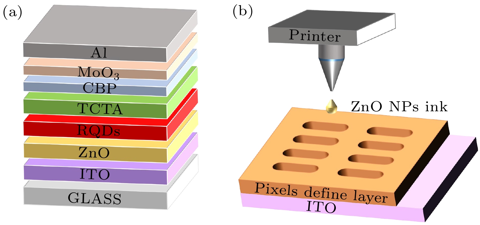
图 1 (a) 发光器件结构示意图; (b) 喷墨打印示意图
Figure 1. (a) Structure of the light-emitting device; (b) diagram of the inkjet printing process.
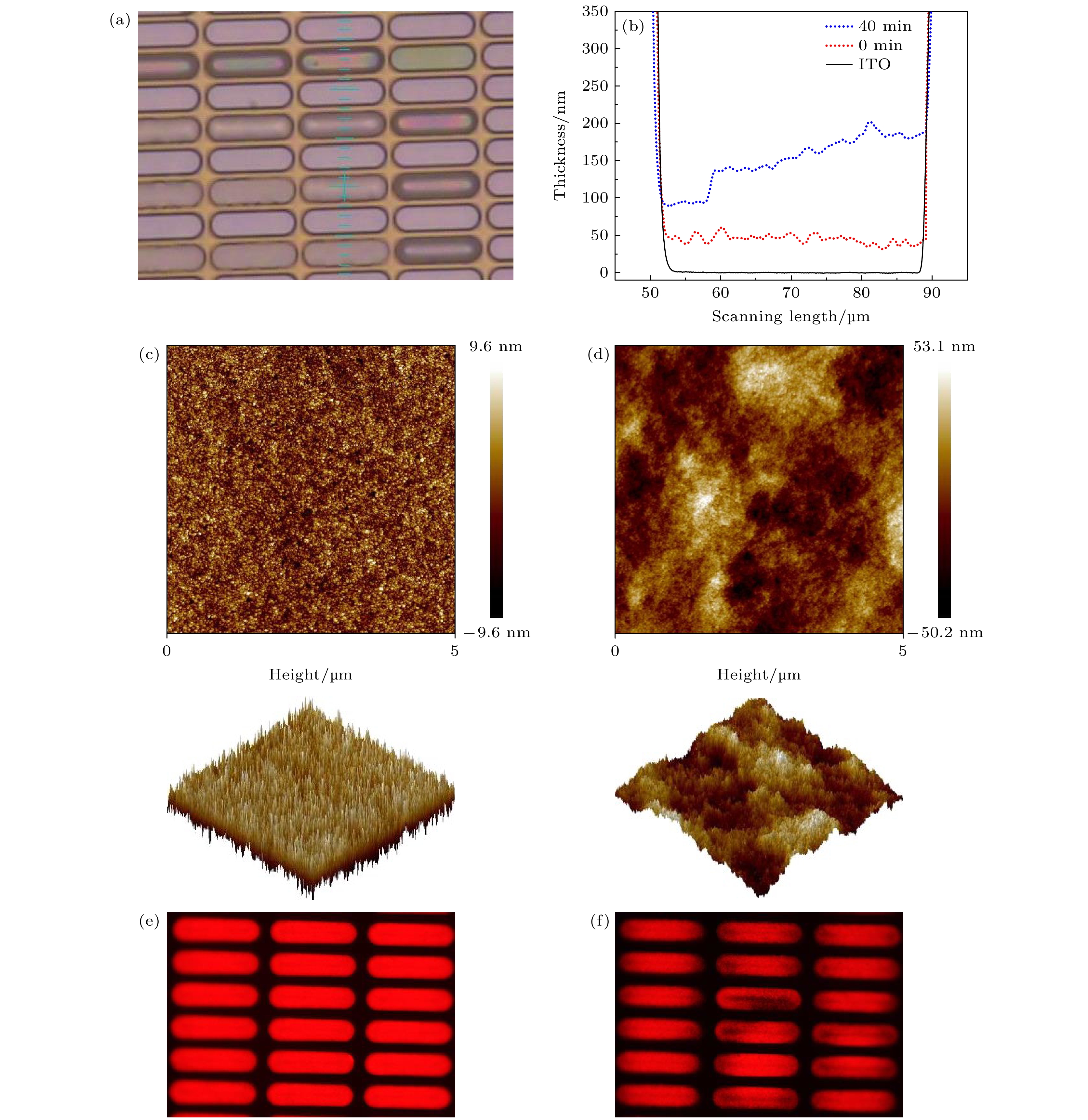
图 2 (a) 打印完成5 min后的显微镜照片; (b) 像素坑中薄膜厚度. 薄膜的AFM图像 (c) 直接进行真空干燥与退火处理; (d) 空气放置40 min后进行干燥退火处理. (e), (f) 所制备的QLED器件在3.8 V工作电压下的电致发光显微镜照片
Figure 2. (a) Microscope photos for 5 min after printing; (b) film thickness in pixel pit. AFM image of the film: (c) Directly vacuum drying and annealing treatment; (d) air placement for 40 min and dry annealing treatment. (e), (f) Electroluminescence microscope photos of the QLED device at 3.8 V operating voltage

图 3 (a)—(c) ZnO薄膜中N, Zn, O元素在氩刻蚀(≈10 nm深度)的XPS光谱. N元素的402.3 eV处峰位面积 (d)与O元素的532 eV峰位面积 (e)随在空气中放置时间的变化(已进行归一化处理)
Figure 3. (a)–(c) XPS spectra of N, Zn and O elements in ZnO films before and after argon etching (≈10 nm depth). Peak area at 402.3 eV of element N (d) and 532 eV of element O (e) as a function of time in air (Normalized).
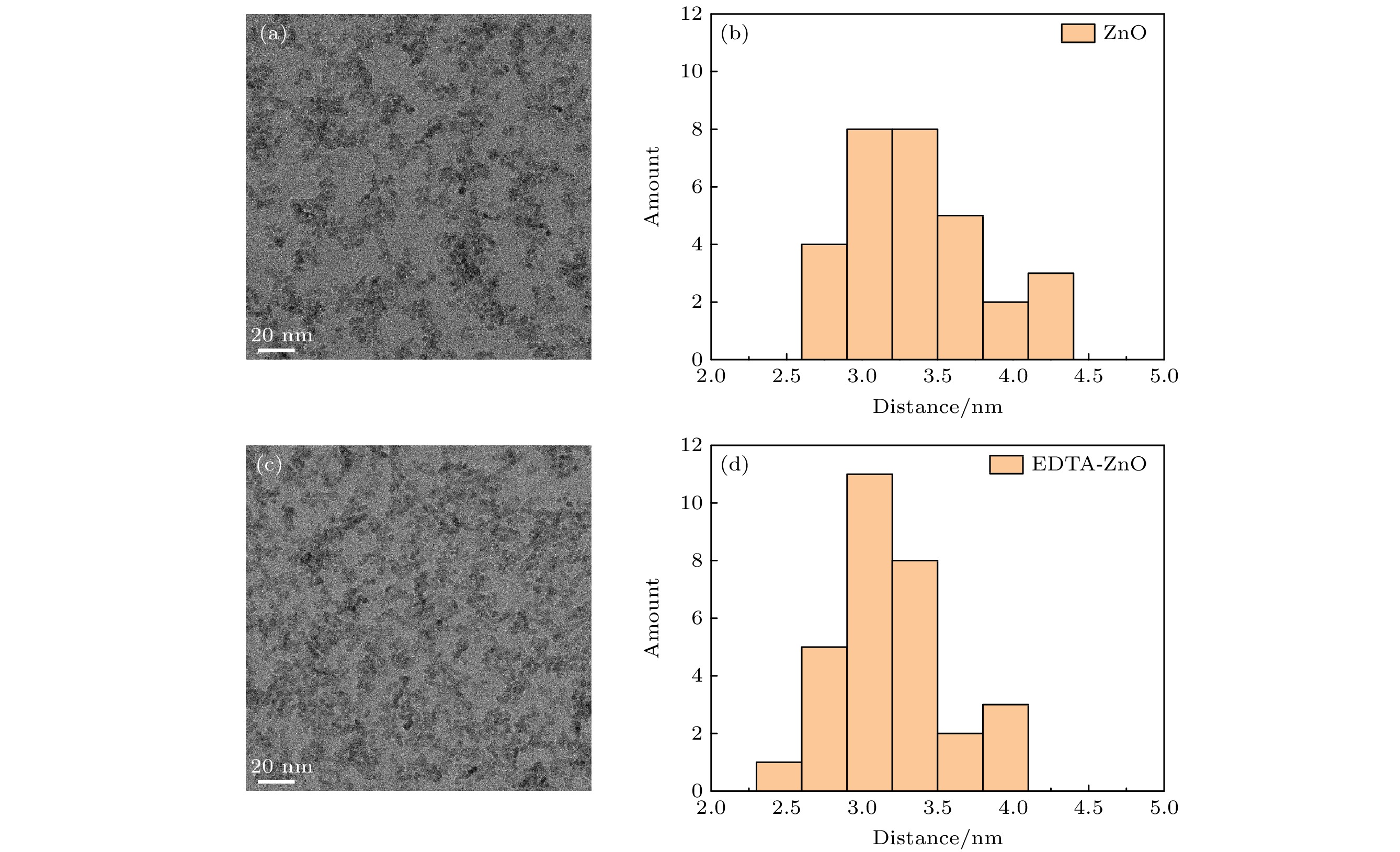
图 4 ZnO量子点与EDTA-ZnO量子点的TEM图(a), (c)与粒径分布图(b), (d)
Figure 4. TEM images of ZnO quantum dots and EDTA-ZnO quantum dots (a), (c), Particle size distribution (b), (d).
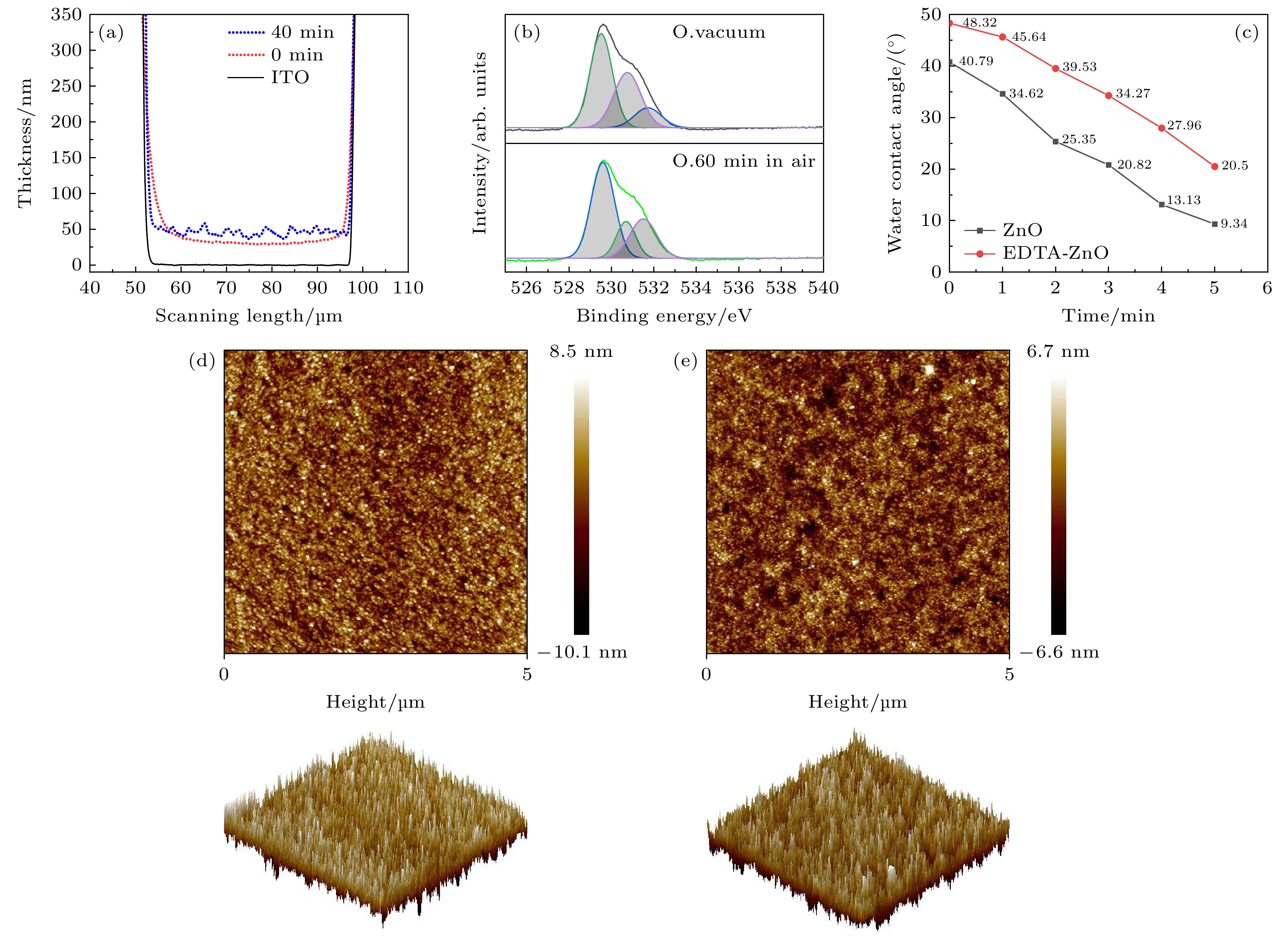
图 5 EDTA-ZnO打印薄膜在直接真空干燥退火与空气中放置40 min后干燥退火 表面轮廓仪图像(a)与AFM图像(d), (e); (b) EDTA-ZnO薄膜中的O元素在氩刻蚀(≈10 nm深度)的XPS光谱; (c) ZnO与EDTA-ZnO薄膜的水接触角随时间变化曲线
Figure 5. Surface profilers image (a) and AFM image (d), (e) of EDTA-ZnO printed film after direct vacuum drying annealing and 40 minutes of drying annealing in air; (b) XPS spectra of O elements in EDTA-ZnO films etched with argon at ≈10 nm depth; (c) water contact angle curve of ZnO and EDTA-ZnO films with time.

图 6 (a) ZnO与EDTA-ZnO薄膜的PL发射谱图; 红光量子点分别在石英基板、ZnO基板、EDTA-ZnO基板上旋涂成膜后的PLQY对比(b)和TRPL曲线(c)
Figure 6. (a) PL emission spectra of ZnO and EDTA-ZnO films; PLQY contrast (b) and TRPL curves (c) of red quantum dots coated on quartz substrate, ZnO substrate and EDTA-ZnO substrate.
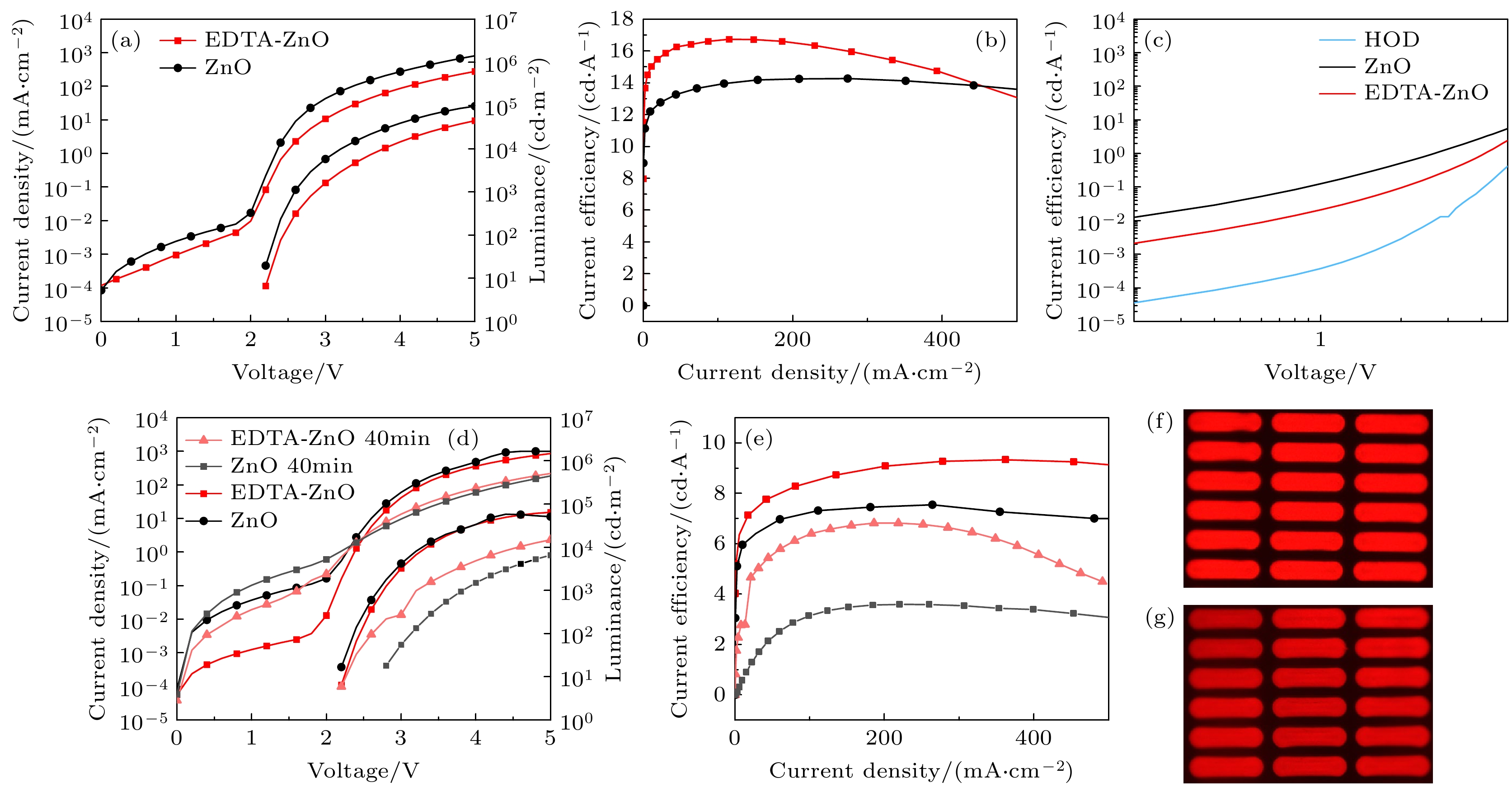
图 7 ZnO与EDTA-ZnO薄膜旋涂器件的J-V-L曲线(a)和CE-L曲线(b); (c) 单载流子器件的J-V曲线; ZnO与EDTA-ZnO薄膜在分别在直接真空干燥退火与空气中放置40 min后干燥退火两种条件下制备喷墨打印器件的J-V-L曲线(d), CE-L曲线(e)以及电致发光显微镜照片(f), (g)
Figure 7. J-V-L curves (a) and CE-L curves (b) of ZnO and EDTA-ZnO thin film spin coating device; (c) J-V curves of single carrier device; J-V-L curves (d), CE-L curves (e), electroluminescence microscope photos (f), (g) of inkjet printing devices prepared by ZnO and EDTA-ZnO thin films after direct vacuum drying annealing and drying annealing in air for 40 min.
表 1 不同条件下的ZnO薄膜中的O和Zn元素含量比
Table 1. Content ratio of O and Zn elements in ZnO thin films under different conditions.
In vacuum 30 min
in air60 min
in air30 min
in N2O/Zn 1.32 2.01 2.48 1.13  DownLoad: CSV
表 2 不同 ETLs 上的 RQDs 瞬态荧光寿命拟合参数
Table 2. Transient fluorescence lifetime fitting parameters of RQDs on different ETLs.
Sample τau/ns A1 τ1/ns A2 τ2/ns Quartz/QDs 62.90 35 15.36 64 89.86 ZnO/QDs 51.14 43 12.54 56 80.31 EDTA-ZnO/QDs 59.61 36 13.67 63 86.34
DownLoad: CSV
表 3 ZnO与EDTA-ZnO薄膜在分别在真空干燥退火与空气中放置40 min后干燥退火两种条件下制备喷墨打印器件的性能
Table 3. Performance of inkjet printing devices prepared by ZnO and EDTA-ZnO films after drying annealing in vacuum and drying annealing after 40 min in air.
ETL Von/V CEmax/
(cd·A–1)Lmax/
(cd·m–2)ZnO 2.2 7.54 53773 EDTA-ZnO 2.2 9.24 64373 ZnO (40 min in air) 2.8 3.59 21474 EDTA-ZnO
(40 min in air)2.2 6.82 22592
DownLoad: CSV
-
[1] Pidluzhna А, Ivaniuk K, Stakhira P, Hotra Z, Chapran M, Ulanski J, Tynkevych O, Khalavka Y, Baryshnikov G V, Minaev B F, Ågren H 2019 Dyes Pigm. 162 647
Google Scholar
[2] Nguyen H T, Duong A T, Lee S 2021 J. Mater. Res. 36 3309
Google Scholar
[3] Sun J, Wang H, Shi H, Wang S, Xu J, Ma J, Ma B, Wen M, Li J, Zhao J, Liu H, Wang Y, Jiang L 2020 ACS Appl. Mater. Interfaces 12 48820
Google Scholar
[4] Song J, Wang O, Shen H, Lin Q, Li Z, Wang L, Zhang X, Li L S 2019 Adv. Funct. Mater. 29 1808377
Google Scholar
[5] Kim T, Kim K H, Kim S, Choi S M, Jang H, Seo H K, Lee H, Chung D Y, Jang E 2020 Nature 586 385
Google Scholar
[6] Zhang W, Ding S, Zhuang W, Wu D, Liu P, Qu X, Liu H, Yang H, Wu Z, Wang K, Sun X W 2020 Adv. Funct. Mater. 30 2005303
Google Scholar
[7] Giuri A, Saleh E, Listorti A, Colella S, Rizzo A, Tuck C, Corcione C E 2019 Nanomaterials 9 582
Google Scholar
[8] Han Y J, Kang K T, Cho K H 2021 ACS Appl. Mater. Interfaces 13 50111
Google Scholar
[9] Chen M, Xie L, Wei C, Yi Y Q Q, Chen X, Yang J, Zhuang J, Li F, Su W, Cui Z 2021 Nano Res. 14 4125
Google Scholar
[10] Zhan S, Suh Y H, Fan X B, Yang J, Ni L, Kim Y, Jo J W, Choi H W, Jung S M, Shin D W, Lee S, Kim J M 2022 J. Soc. Inf. Display 30 748
Google Scholar
[11] Yang P, Zhang L, Kang D J, Strahl R, Kraus T 2020 Adv. Opt. Mater. 8 1901429
Google Scholar
[12] Xiong X, Wei C, Xie L, Chen M, Tang P, Shen W, Deng Z, Li X, Duan Y, Su W, Zeng H, Cui Z 2019 Org. Electron. 73 247
Google Scholar
[13] Liu Y, Li F, Xu Z, Zheng C, Guo T, Xie X, Qian L, Fu D, Yan X 2017 ACS Appl. Mater. Interfaces 9 25506
Google Scholar
[14] Han J, Ko D, Park M, Roh J, Jung H, Lee Y, Kwon Y, Sohn J, Bae W K, Chin B D, Lee C 2016 J. Soc. Inf. Display 24 545
Google Scholar
[15] Adnan R H, Woon K L, Chanlek N, Nakajima H, Abd Majid W H 2017 Aust. J. Chem. 70 1110
Google Scholar
[16] Wang Q, Sun Q, Jena P 2008 J. Chem. Phys. 129 164714
Google Scholar
[17] Wu Y, Li X, Wei S, Liu Y, Ma M Y, Huang L J, Pan D C 2019 Mater. Res. Express 6 085060
Google Scholar
[18] Fragalà M E, Aleeva Y, Malandrino G 2010 Superlattices Microstruct. 48 408
Google Scholar
[19] Wang Z, Mahoney C, Yan J, Lu Z, Ferebee R, Luo D, Bockstaller M R, Matyjaszewski K 2016 Langmuir 32 13207
Google Scholar
[20] Zanjani S M, Tintori F, Sadeghi S, Linkov P, Dayneko S, Shahalizad A, Pahlevaninezhad H, Pahlevani M 2022 Adv. Photonics Res. 3 2200159
Google Scholar
[21] Lee Y, Jeong B G, Roh H, Roh J, Han J, Lee D C, Bae W K, Kim J Y, Lee C 2018 Adv. Quantum Technol. 1 1700006
Google Scholar
[22] Chen H, Ding K, Fan L, Zhang R, Guo R, Zhang J, Hou L, Wang L 2022 J. Mater. Chem. C 10 8373
Google Scholar
[23] Dai X, Zhang Z, Jin Y, Niu Y, Cao H, Liang X, Chen L, Wang J, Peng X 2014 Nature 515 96
Google Scholar
[24] Jo Y J, Kim S Y, Hyun J H, Park B, Choy S, Koirala G R, Kim T I 2022 Npj Flexible Electron. 6 31
Google Scholar
[25] Kaneva N, Stambolova I, Blaskov V, Dimitriev Y, Vassilev S, Dushkin C 2010 J. Alloys Compd. 500 252
Google Scholar
[26] Moreira N H, Domıinguez A, Frauenheim T, da Rosa A L 2012 Phys. Chem. Chem. Phys. 14 15445
Google Scholar
[27] Bai S, Jin Y, Liang X, Ye Z, Wu Z, Sun B, Ma Z, Tang Z, Wang J, Würfel U, Gao F, Zhang F 2015 Adv. Energy Mater. 5 1401606
Google Scholar
[28] Li X, Liu X, Zhang W, Wang H Q, Fang J 2017 Chem. Mater. 29 4176
Google Scholar
[29] Bae W K, Park Y S, Lim J, Lee D, Padilha L A, McDaniel H, Robel I, Lee C, Pietryga J M, Klimov V I 2013 Nat. Commun. 4 2661
Google Scholar
[30] Wang H C, Zhang H, Chen H Y, Yeh H C, Tseng M R, Chung R J, Chen S, Liu R S 2017 Small 13 1603962
Google Scholar

 DownLoad:
Catalog
Metrics
- Abstract views: 1801
- PDF Downloads: 69
- Cited By: 0
