


-
In this paper, the displacement damage degradation characteristics of silicon carbide (SiC) Schottky barrier diode (SBD) and metal oxide semiconductor field effect transistor (MOSFET) are studied under 14-MeV neutron irradiation. The experimental results show that the neutron irradiation with a total fluence of 1.18×1011 cm–2 will not cause notable degradation of the forward I-V characteristics of the diode, but will lead to a significant increase in the reverse leakage current. A defect with energy level position of
$ E_{\rm{C}} - 1.034 $ eV is observed after irradiation by deep level transient spectroscopy (DLTS) testing, which is corresponding to the neutron-induced defect cluster in SiC. This deep level defect may cause the Fermi level of n-type doping drift region to move toward the mid-gap level. It ultimately results in the decrease of the Schottky barrier and the increase of the reverse leakage current. In addition, neutron-induced gate leakage increase is also observed for SiC MOSFET. The gate current corresponding to Vgs = 15 V after irradiation increases nearly 3.3 times that before irradiation. The donor-type defects introduced by neutron irradiation in the oxide layer result in the difference in the conductivity mechanism of gate oxygen between before and after irradiation. The defects have an auxiliary effect on carrier crossing the gate oxide barrier, which leads to the increase of gate leakage current. The defects introduced by neutron irradiation are neutral after capturing electrons. The trapped electrons can cross a lower potential well and enter the conduction band to participate in conduction when the gate is positively biased, thus causing the gate current to increase with the electric field increasing. After electrons captured by donor-type defects enter the conduction band, positively charged defects are left from the gate oxide, leading to the negative shift of the transfer characteristics of SiC MOSFET. The results of DLTS testing indicate that the neutron irradiation can not only cause the intrinsic defect state of SiC material to change near the channel of MOSFET, but also give rise to new silicon vacancy defects. However, these defects are not the main cause of device performance degradation due to their low density relative to the intrinsic defect’s.-
Keywords:
- silicon carbide power device /
- neutron irradiation /
- displacement damage /
- deep level transient spectrum
[1] Casady J B, Johnson R W 1996 Solid State Electron. 39 1409
 Google Scholar
[2] Kimoto T, Cooper J A 2014 Fundamentals of Silicon Carbide Technology: Growth, Characterization, Devices and Applications (Singapore: John Wiley & Sons) p16
[3] 张林, 肖剑, 邱彦章, 程鸿亮 2011 物理学报 60 056106
Google Scholar
Zhang L, Xiao J, Qiu Y Z, Cheng H L 2011 Acta Phys. Sin. 60 056106
Google Scholar
[4] 张鸿, 郭红霞, 潘霄宇, 雷志锋, 张凤祁, 顾朝桥, 柳奕天, 琚安安, 欧阳晓平 2021 物理学报 70 162401
Google Scholar
Zhang H, Guo H X, Pan X Y, Lei Z F, Zhang F Q, Gu Z Q, Liu Y T, Ju A A, Ouyang X P 2021 Acta Phys. Sin. 70 162401
Google Scholar
[5] Yu C H, Wang Y, Bao M T, Li X J, Yang J Q, Tang Z H 2021 IEEE Trans. Electron Dev. 68 5034
Google Scholar
[6] Yu C H, Wang Y, Li X J, Liu C M, Luo X, Cao F 2018 IEEE Trans. Electron Dev. 65 5434
Google Scholar
[7] McPherson J A, Kowal P J, Pandey G K, Chow T P, Ji W, Woodworth A A 2019 IEEE Trans. Nucl. Sci. 66 474
Google Scholar
[8] Ball D R, Hutson J M, Javanainen A, Lauenstein J M, Galloway K F, Johnson R A, Alles M L, Sternberg A L, Sierawski B D, Witulski A F, Reed R A, Schrimpf R D 2020 IEEE Trans. Nucl. Sci. 67 22
Google Scholar
[9] 彭超, 雷志锋, 张战刚, 何玉娟, 陈义强, 路国光, 黄云 2022 物理学报 71 176101
Google Scholar
Peng C, Lei Z F, Zhang Z G, He Y J, Chen Y Q, Lu G G, Huang Y 2022 Acta Phys. Sin. 71 176101
Google Scholar
[10] Steffens M, Höffgen S K, Poizat M 2017 17th European Conference on Radiation and its Effects on Components and Systems ( RADECS) Geneva, Switzerland, October 2–6, 2017 p1
[11] Akturk A, McGarrity J M, Potbhare S, Goldsman N 2012 IEEE Trans. Nucl. Sci. 59 3258
Google Scholar
[12] Zhang C X, Zhang E X, Fleetwood D M, Schrimpf R D, Dhar S, Ryu S H, Shen X, Pantelides S T 2011 IEEE Trans. Nucl. Sci. 58 2925
Google Scholar
[13] Hazdra P, Záhlava V, Vobecký J 2014 Nucl. Instr. Meth. Phys. Res. B 327 124
Google Scholar
[14] Omotoso E, Meyer W E, Auret F D, Paradzah A T, Legodi M J 2016 Nucl. Instr. Meth. Phys. Res. B 371 312
Google Scholar
[15] Yang J, Li H, Dong S, Li X 2019 IEEE Trans Nucl. Sci. 66 2042
Google Scholar
[16] Chao D S, Shih H Y, Jiang J Y, et al 2019 Jap. J. Appl. Phys. 58 SBBD08
Google Scholar
[17] Agostinelli S, Allison J, Amako K, et al 2003 Nucl. Instr. Meth. Phys. Res. A 506 250
Google Scholar
[18] Allison J, Amako K, Apostolakis J, et al 2006 IEEE Trans. Nucl. Sci. 53 270
Google Scholar
[19] 巴利加 著 (韩郑生 等 译) 2013 功率半导体器件基础 (北京: 电子工业出版社) 第99—101页
Baliga B J (translated by Han Z S, et al) 2013 Fundamentals of Power Semiconductor Devices (Beijing: Publishing House of Electronics Industry) pp99–101
[20] Castaldini A, Cavallini A, Polenta L, Nava F, Canali C, Lanzieri C 2002 Appl. Surf. Sci. 187 248
Google Scholar
[21] Dalibor T, Pensl G, Matsunami H, Kimoto T, Choyke W J, Schoner A, Nordell N 1997 Phys. Stat. Sol. (a) 162 199
Google Scholar
[22] Alfieri G, Mihaila A, Nipoti R, Puzzanghera M, Sozzi G, Godignon P, Millán J 2017 Materials Science Forum 897 246
Google Scholar
[23] Alfieri G, Monakhov E V, Svensson B G, Hallén A 2005 J. Appl. Phys. 98 113524
Google Scholar
[24] 施敏, 伍国珏 著 (耿莉, 张瑞智 译) 2008 半导体器件物理 (西安: 西安交通大学出版社) 第173—176页
Sze S M, Ng K K (translated by Geng L, Zhang R Z) 2008 Physics of Semiconductor Devices (Xi’an: Xi’an Jiaotong University Press) pp173–176
-
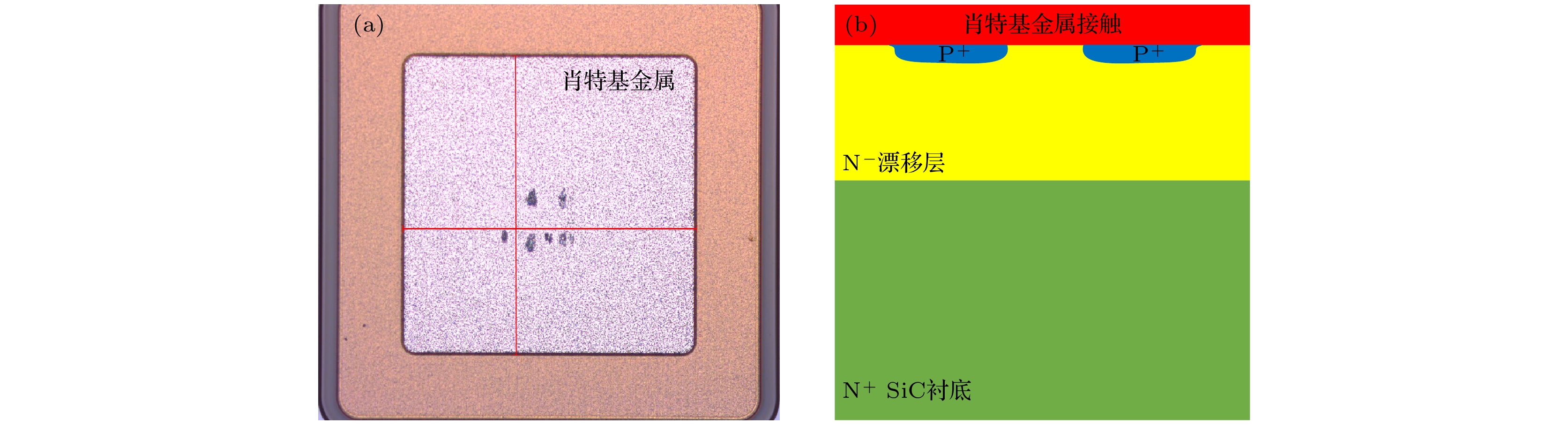
图 1 试验用SiC结势垒肖特基二极管器件 (a)表面形貌的光学显微镜图; (b)截面示意图
Figure 1. SiC JBS diode used in our experiment: (a) Optical microscope diagram of surface morphology; (b) diagram of cross-section.

图 2 试验用SiC MOSFET器件 (a)表面形貌的光学显微镜图; (b)截面示意图
Figure 2. SiC MOSFET used in our experiment: (a) Optical microscope diagram of surface morphology; (b) diagram of cross-section.

图 3 额定电压为650 V的二极管辐照前后正向(a)和反向(b) I-V特性
Figure 3. Forward (a) and reverse (b) I-V characteristics of 650 V SiC diode before and after irradiation.

图 5 额定电压为1700 V的二极管辐照前后正向(a)和反向(b)I-V特性
Figure 5. Forward (a) and reverse (b) I-V characteristics of 1700 V SiC diode before and after irradiation.

图 4 额定电压为1200 V的二极管辐照前后正向(a)和反向(b) I-V特性
Figure 4. Forward (a) and reverse (b) I-V characteristics of 1200 V SiC diode before and after irradiation.

图 6 (a)额定电压为1700 V的二极管辐照前后的深能级瞬态谱特性, 其中内嵌图为温度300—400 K之间曲线的放大图; (b)阿伦尼乌斯曲线
Figure 6. (a) DLTS spectra of 1700 V SiC diode before and after irradiation, the inset graph is the enlarged curve between 300–400 K; (b) Arrhenius plot.

图 7 DLTS测试过程中SiC二极管的能带示意图(EV为价带能级) (a)辐照前; (b)辐照后.
Figure 7. Schematic diagram of the energy band of SiC diode during DLTS testing process: (a) Pre-irradiation; (b) after-irradiation.

图 8 (a) SiC MOSFET器件辐照前后的转移特性和栅电流特性, 测试条件为源端电压Vs = 0 V, 漏端电压Vd = 0.1 V; (b)辐照后SiC MOSFET器件栅电流拟合, 测试条件Vd = Vs = 0 V
Figure 8. (a) Transfer and gate-current characteristics of SiC MOSFET before and after irradiation (test condition, Vs = 0 V, Vd = 0.1 V); (b) gate current fitting of SiC MOSFET after irradiation (test condition Vd = Vs = 0 V).
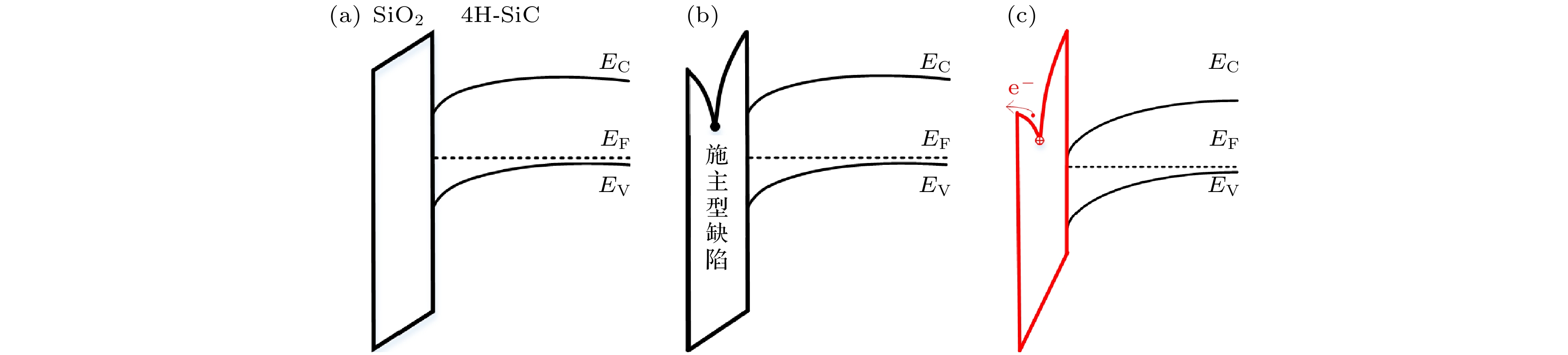
图 9 (a)辐照前未加栅偏压下的SiC MOSFET器件能带图; (b)辐照后未加栅偏压下的SiC MOSFET器件能带图; (c)辐照后加正栅偏压下的SiC MOSFET器件能带图
Figure 9. (a) Energy band diagram of SiC MOSFET without gate bias before irradiation; (b) energy band diagram of SiC MOSFET without gate bias after irradiation; (c) energy band diagram of SiC MOSFET with positive gate bias after irradiation.

图 10 (a)辐照前后SiC功率MOSFET器件的深能级瞬态谱; (b)阿伦尼乌斯曲线
Figure 10. (a) DLTS spectrums of SiC MOSFET before and after irradiation; (b) Arrhenius plot.
表 1 根据I-V特性提取的二极管肖特基势垒高度
Table 1. Schottky barrier height of SiC diodes extracted by I-V characteristics.
器件 650 V器件 1200 V器件 1700 V器件 辐照前 辐照后 辐照前 辐照后 辐照前 辐照后 肖特基势垒 ΦB0/eV 1.224 1.214 1.220 1.209 1.203 1.194 理想因子 n 1.02 1.03 1.02 1.03 1.02 1.03  DownLoad: CSV
表 2 基于深能级瞬态谱提取的SiC二极管辐照前后的缺陷信息
Table 2. Trap information of SiC diode extracted by DLTS before and after irradiation.
缺陷类型 缺陷DT1 缺陷DT2 能级EC-ET/eV 缺陷密度/cm–3 俘获截面/cm2 能级EC-ET/eV 缺陷密度/cm–3 俘获截面/cm2 辐照前 0.071 8.60×10¹³ 2.55×10⁻²³ 0.864 3.29×10¹² 2.19×10⁻¹⁵ 辐照后 0.052 8.09×10¹³ 3.21×10⁻²³ 1.034 3.47×10¹² 8.34×10⁻¹³
DownLoad: CSV
表 3 基于深能级瞬态谱提取的SiC MOSFET辐照前后的缺陷信息
Table 3. Trap information of SiC MOSFET extracted by DLTS before and after irradiation.
缺陷类型 缺陷MT1 缺陷MT2 能级EC-ET/eV 缺陷密度/cm–3 俘获截面/cm2 能级EC-ET/eV 缺陷密度/cm–3 俘获截面/cm2 辐照前 1.112 1.42×10¹⁴ 8.60×10⁻⁹ — — — 辐照后 0.980 1.59×10¹⁴ 2.82×10⁻¹⁰ 0.376 1.34×10¹³ 6.31×10⁻¹⁷
DownLoad: CSV
-
[1] Casady J B, Johnson R W 1996 Solid State Electron. 39 1409
Google Scholar
[2] Kimoto T, Cooper J A 2014 Fundamentals of Silicon Carbide Technology: Growth, Characterization, Devices and Applications (Singapore: John Wiley & Sons) p16
[3] 张林, 肖剑, 邱彦章, 程鸿亮 2011 物理学报 60 056106
Google Scholar
Zhang L, Xiao J, Qiu Y Z, Cheng H L 2011 Acta Phys. Sin. 60 056106
Google Scholar
[4] 张鸿, 郭红霞, 潘霄宇, 雷志锋, 张凤祁, 顾朝桥, 柳奕天, 琚安安, 欧阳晓平 2021 物理学报 70 162401
Google Scholar
Zhang H, Guo H X, Pan X Y, Lei Z F, Zhang F Q, Gu Z Q, Liu Y T, Ju A A, Ouyang X P 2021 Acta Phys. Sin. 70 162401
Google Scholar
[5] Yu C H, Wang Y, Bao M T, Li X J, Yang J Q, Tang Z H 2021 IEEE Trans. Electron Dev. 68 5034
Google Scholar
[6] Yu C H, Wang Y, Li X J, Liu C M, Luo X, Cao F 2018 IEEE Trans. Electron Dev. 65 5434
Google Scholar
[7] McPherson J A, Kowal P J, Pandey G K, Chow T P, Ji W, Woodworth A A 2019 IEEE Trans. Nucl. Sci. 66 474
Google Scholar
[8] Ball D R, Hutson J M, Javanainen A, Lauenstein J M, Galloway K F, Johnson R A, Alles M L, Sternberg A L, Sierawski B D, Witulski A F, Reed R A, Schrimpf R D 2020 IEEE Trans. Nucl. Sci. 67 22
Google Scholar
[9] 彭超, 雷志锋, 张战刚, 何玉娟, 陈义强, 路国光, 黄云 2022 物理学报 71 176101
Google Scholar
Peng C, Lei Z F, Zhang Z G, He Y J, Chen Y Q, Lu G G, Huang Y 2022 Acta Phys. Sin. 71 176101
Google Scholar
[10] Steffens M, Höffgen S K, Poizat M 2017 17th European Conference on Radiation and its Effects on Components and Systems ( RADECS) Geneva, Switzerland, October 2–6, 2017 p1
[11] Akturk A, McGarrity J M, Potbhare S, Goldsman N 2012 IEEE Trans. Nucl. Sci. 59 3258
Google Scholar
[12] Zhang C X, Zhang E X, Fleetwood D M, Schrimpf R D, Dhar S, Ryu S H, Shen X, Pantelides S T 2011 IEEE Trans. Nucl. Sci. 58 2925
Google Scholar
[13] Hazdra P, Záhlava V, Vobecký J 2014 Nucl. Instr. Meth. Phys. Res. B 327 124
Google Scholar
[14] Omotoso E, Meyer W E, Auret F D, Paradzah A T, Legodi M J 2016 Nucl. Instr. Meth. Phys. Res. B 371 312
Google Scholar
[15] Yang J, Li H, Dong S, Li X 2019 IEEE Trans Nucl. Sci. 66 2042
Google Scholar
[16] Chao D S, Shih H Y, Jiang J Y, et al 2019 Jap. J. Appl. Phys. 58 SBBD08
Google Scholar
[17] Agostinelli S, Allison J, Amako K, et al 2003 Nucl. Instr. Meth. Phys. Res. A 506 250
Google Scholar
[18] Allison J, Amako K, Apostolakis J, et al 2006 IEEE Trans. Nucl. Sci. 53 270
Google Scholar
[19] 巴利加 著 (韩郑生 等 译) 2013 功率半导体器件基础 (北京: 电子工业出版社) 第99—101页
Baliga B J (translated by Han Z S, et al) 2013 Fundamentals of Power Semiconductor Devices (Beijing: Publishing House of Electronics Industry) pp99–101
[20] Castaldini A, Cavallini A, Polenta L, Nava F, Canali C, Lanzieri C 2002 Appl. Surf. Sci. 187 248
Google Scholar
[21] Dalibor T, Pensl G, Matsunami H, Kimoto T, Choyke W J, Schoner A, Nordell N 1997 Phys. Stat. Sol. (a) 162 199
Google Scholar
[22] Alfieri G, Mihaila A, Nipoti R, Puzzanghera M, Sozzi G, Godignon P, Millán J 2017 Materials Science Forum 897 246
Google Scholar
[23] Alfieri G, Monakhov E V, Svensson B G, Hallén A 2005 J. Appl. Phys. 98 113524
Google Scholar
[24] 施敏, 伍国珏 著 (耿莉, 张瑞智 译) 2008 半导体器件物理 (西安: 西安交通大学出版社) 第173—176页
Sze S M, Ng K K (translated by Geng L, Zhang R Z) 2008 Physics of Semiconductor Devices (Xi’an: Xi’an Jiaotong University Press) pp173–176


 DownLoad:
Catalog
Metrics
- Abstract views: 1869
- PDF Downloads: 67
- Cited By: 0
