


-
In this work, a system of modified Mott-Gurney differential equations is based on Arrhenius’ law and the overpotential theory of ionic motion in bipolar electrochemical metallization (ECM) resistive devices. The average displacement of ions is solved by the modified Mott-Gurney equation. Then, the relation between the average displacement and the growth length of the conductive filament is obtained by a geometric model based on cells. The equation of applied voltage versus Forming/Set time and the equation of length of conductive filament growth versus time are deduced by using this relation. In this work, an algorithm for extracting kinetic parameters of ions in a bipolar ECM device is also proposed. By using this algorithm, the characteristics of the applied voltage versus Forming/Set time for Ag/γ-AgI/Pt, Ag/TiO2/Pt, Ag/GeS2/W, and Cu/SiO2/Au devices are calculated and the calculation results are consistent with experimental data. It is found that in the Forming/Set process, the jump step of silver ion is the lattice constant along the c direction of a unit cell of the crystal for TiO2 and the lattice constant of the cubic, a, for γ-AgI. These results are explained in the following. In a unit cell of the two crystals there are some tetrahedral and octahedral interstitial sites. The cationic motion path consists of alternating octahedral and tetrahedral sites or some octahedral sites. The cation jumps from tetrahedron to octahedron to tetrahedron, etc. in the γ-AgI with coplanar polyhedron and from octahedron to octahedron in the TiO2 with edge shared octahedron. In GeS2 crystal, it is found that the jump step of silver ions is the lattice constant in the c direction of a unit cell. Owing to the periodicity of the lattice, the pathways of the ion motion in the three materials can be expressed by a periodic potential barrier each. For the jump situation of the copper ion in amorphous SiO2, the jump step of copper ions is calculated to be 1.57 times the length of the O—O bond, and the jump pathway can also be explained by a periodic potential barrier. By introducing the cosine potential barrier, the ionic activation frequency, potential barrier height, ionic mobility and diffusion coefficient, and characteristics of the conductive filament growth versus time in several devices are calculated. The criteria of selecting dielectric materials for bipolar ECM devices are discussed by using these data. It is found that the standards for selecting dielectric materials of bipolar ECM devices are the ion activation energy ≤0.5 eV, preferably between 0.1–0.2eV, and the DC conductivity as close to 10 –4 Ω–1·cm–1 as possible. -
Keywords:
- bipolar resistive memory /
- Forming/Set time /
- conductive filament /
- jump step and potential barrier
[1] Aziza H, Jeremy P P , Bazzi H, Canet P, Moreau M, Marca V D, Harb A T 2020 IEEE Trans. Nanotechnol. 19 214
 Google Scholar
[2] Jameson J R, Gilbert N, Koushan F, Wang J, Hollmer S, Kozicki M 2012 Appl. Phys. Lett. 100 023505
Google Scholar
[3] Yu S, Wong P H S 2011 IEEE Trans. Electron. Devices 58 1352
Google Scholar
[4] Hurk J V D, Menzel S, Waser R, Valov I 2015 J. Phys. Chem. C 119 18678
Google Scholar
[5] Covi E, Wang W, Lin Y H, Farronato M, Ambrosi E, Lelmini D 2021 IEEE Trans. Electron. Devices 68 4335
Google Scholar
[6] Valov I, Waser R, Jameson J R, Kozicki M N 2011 Nanotechnology 22 254003
Google Scholar
[7] Lin S, Zhao L, Zhang J Y, Wu H Q, Qian H, Yu Z P 2012 IEEE 2012 International Electron Devices Meeting (IEDM) San Fransisco, USA, December 10−12, 2012 p593
[8] Mott P F, Gurney R W (translated by Pan J S, Li W X) 1953 Electronic Processes in Ionic Crysrals (2nd Ed.) (Bejing: Science Press) p51 (in Chinse) [莫特N F, 格尼R W 著 (潘金声, 李文雄 译) 1959 离子晶体中的电子过程 (北京: 科学出版社) 第51页
Mott P F, Gurney R W (translated by Pan J S, Li W X) 1953 Electronic Processes in Ionic Crysrals (2nd Ed.) (Bejing: Science Press) p51 (in Chinse) [莫特N F, 格尼R W 著 (潘金声, 李文雄 译) 1959 离子晶体中的电子过程 (北京: 科学出版社) 第51页] [9] Zhu J D, Zhang T, Yang Y C, Huang R 2020 Appl. Phys. Rev. 7 011312
Google Scholar
[10] Zhang M Y, Wang G M, Long S B, et al. 2015 IEEE Electron. Device Lett. 36 1303
Google Scholar
[11] Anderson O L, Stuart D A 1954 J. Am. Ceram. Soc. 37 573
Google Scholar
[12] Patnaik J R G, Sunandana C S 1998 J. Phys. Chrn, Solids 59 1059
Google Scholar
[13] Tapperrtzhofen S, Valov I, Waser R 2012 Nanotechnology 23 145703
Google Scholar
[14] Po C, Liao H W, Gan J Y, et al. 2010 ACS Nanotech. 4 5414
Google Scholar
[15] Bermard Y, Gonon P, Jousseaume V 2010 J. Appl. Phys. Lett. 96 193502
Google Scholar
[16] 哈根穆勒P 著 (陈立泉, 薛荣坚 译) 1984 固体电解质一般原理、特征、材料和应用 (北京: 科学出版社) 第29页
Hagenmuller P (translated by Chen L Q, Xue R J) 1984 Solid Electrolytes General Principles, Characterization, Materials, Applications (Bejing: Science Press) p29
[17] Bid A, Bora A, Raychaudhuri A 2006 Phys. Rev. B 74 035426
Google Scholar
[18] Mehrer H 2014 Diffusion in Solids: Fundamentals, Methods, Materials, Diffusion-Controlled Process (New York: Springer Berlin) pp62, 63, 475
[19] 刘明 2018新型阻变存储技术 (北京: 科学出版社) 第88页
Liu M 2018 New Resistive Variable Storage Technology (Beijing: Science Press) p88
[20] 史美仑 1982固体电解质 (重庆: 科学技术文献出版社重庆分社) 第242, 243页
Shi M L 1982 Solid Electrolyte (Chongqing: Chongqing Branch of Science and Technology Literature Press) pp242, 243
[21] Ajayi O B, Nagel L E, Raistrick I D, Huggins R A 1976 J. Phys. Chem. Solids 37 167
Google Scholar
[22] 冯端, 冯晓彤 2005熵的世界 (北京: 科学出版社) 第213页
Feng D, Feng S T 2005 The world of Entropy (Bejing: Science Press) p213
[23] Nowotny M K, Bak T, Nowotny J 2006 J. Phys. Chem. B 110 16271
Google Scholar
[24] Palma G, Vianello E, Cagli C, Molas G, Reyboz M, Blaise P, B. Salvo D, Longnos F, Dahmani F 2012 4th IEEE International Memory Workshop Milan, Italy, May 20−23, 2012 p1
[25] 管绍茂, 王迅 1981半导体表面钝化技术及其应用 (北京: 国防工业出版社) 第70页
Guan S M, Wang X 1981 Semiconductor Surface Passivation Technology and its Application (Bejing: National Defence Industry Press) p70
[26] 哈根穆勒P 著 (陈立泉, 薛荣坚 译) 1984 固体电解质一般原理、特征、材料和应用 (北京: 科学出版社) 第7页
Hagenmuller P (translated by Chen L Q, Xue R J) 1984 Solid Electrolytes General Principles, Characterization, Materials, Applications (Bejing: Science Press) p7
[27] Gao Y R, Adelaide M, Nolan M, Du P, Wu Y F, Yang C, Chen Q L, Mo Y, Bo S H 2020 Chem. Rev. 120 5954
Google Scholar
[28] Shen Z J, Zhao C , Qi Y F, Xu W Y, Liu T, Mitrovic I Z, Yang L, Zhao C 2020 Nanomaterials 10 1437
Google Scholar
[29] Wang W, Covi E K, Lin Y H , Ambrosi E, Milozzi A D, Sbandati C, Farronato M, Ielmini D 2021 IEEE Trans. Electron. Devices 68 4342
Google Scholar
[30] Saadi M, Gonon P, Vallée1 C, Jomni F, Jalaguier E 2020 J. Mater. Sci.-Mater. El. 31 13487
Google Scholar
-
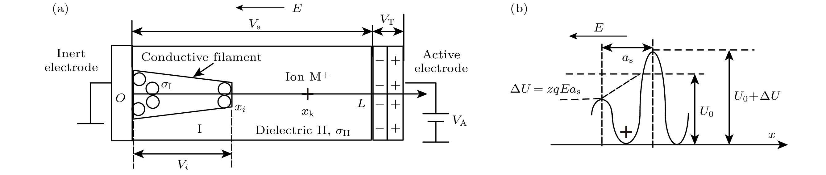
图 1 (a) 从阴极往阳极生长的导电细丝示意图; (b)阳离子跃迁势垒的示意图
Figure 1. (a) Schematic diagram of the conductive filament that grows from the anode to the cathode; (b) schematic diagram of the potential barrier after applying electric field.

图 2 基于cell 的模型
Figure 2. Model based on cells.
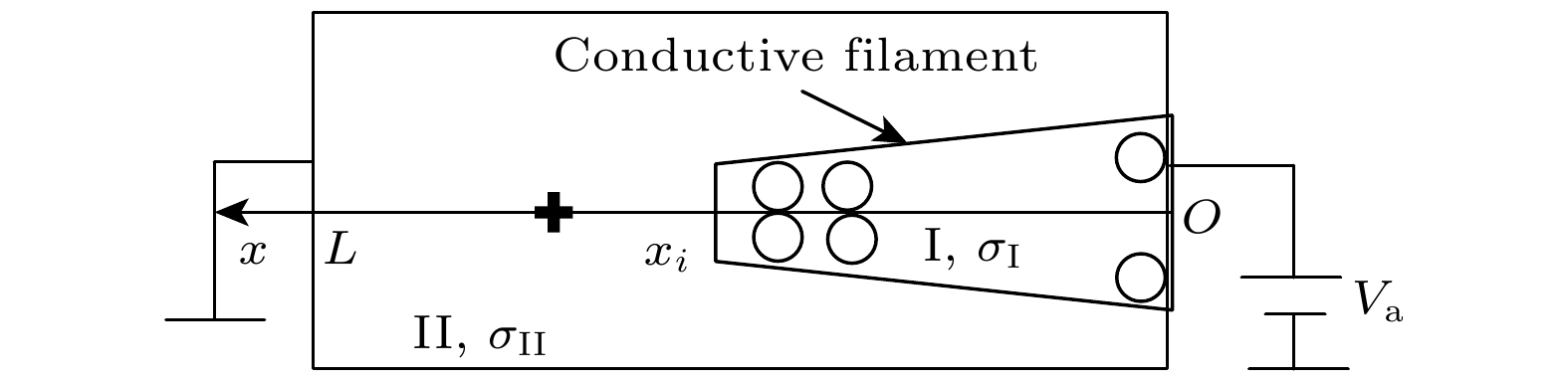
图 3 从阳极往阴极生长的导电细丝示意图
Figure 3. Conductive filament that grows from the cathode to the anode.
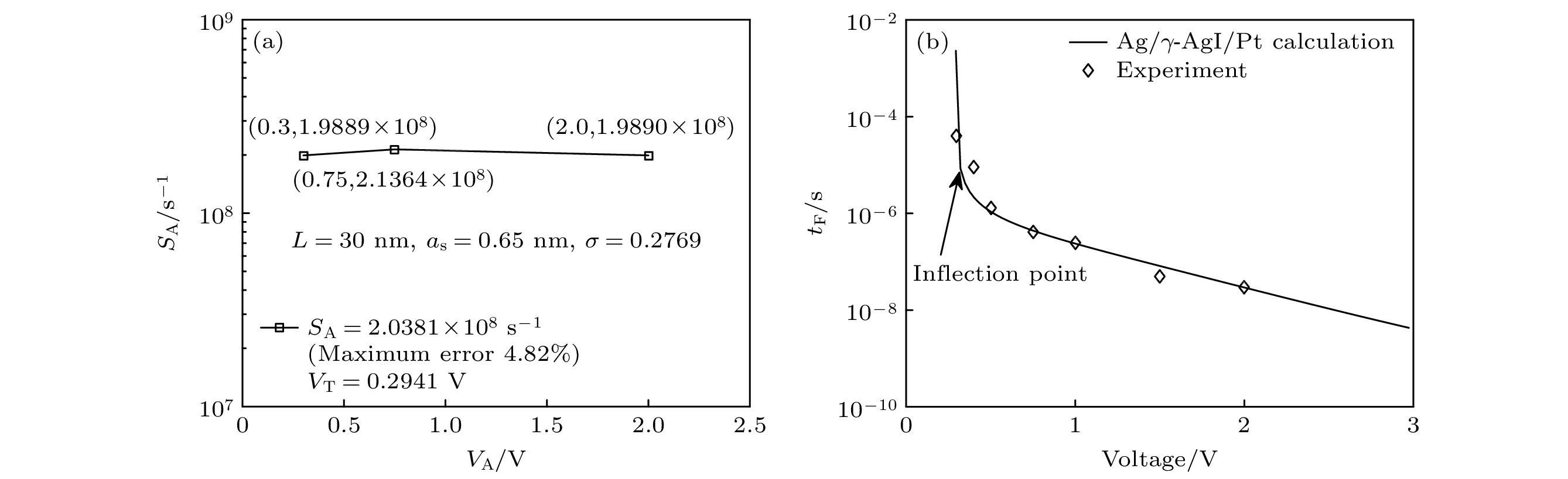
图 4 (a) Ag+在γ-AgI膜中的跃迁速率计算图, 跃迁速率的平均值是2.0381×10⁸ s–1, 最大误差是跃迁速率的3个计算值对于平均值的最大误差; (b) Ag/γ-AgI/Pt的Forming/Set时间与不同外加电压的关系, 其中实验数据见文献[13]
Figure 4. (a) Calculative results of the jump rate for the Ag+ in γ-AgI film. The average value of three jump rates is 2.0381×10⁸ s–1 and the maximum error is the maximum error for three jump rates relative to the average value. (b) The applied voltage of the device versus the Forming/Set time. The experimental data see Ref. [13].
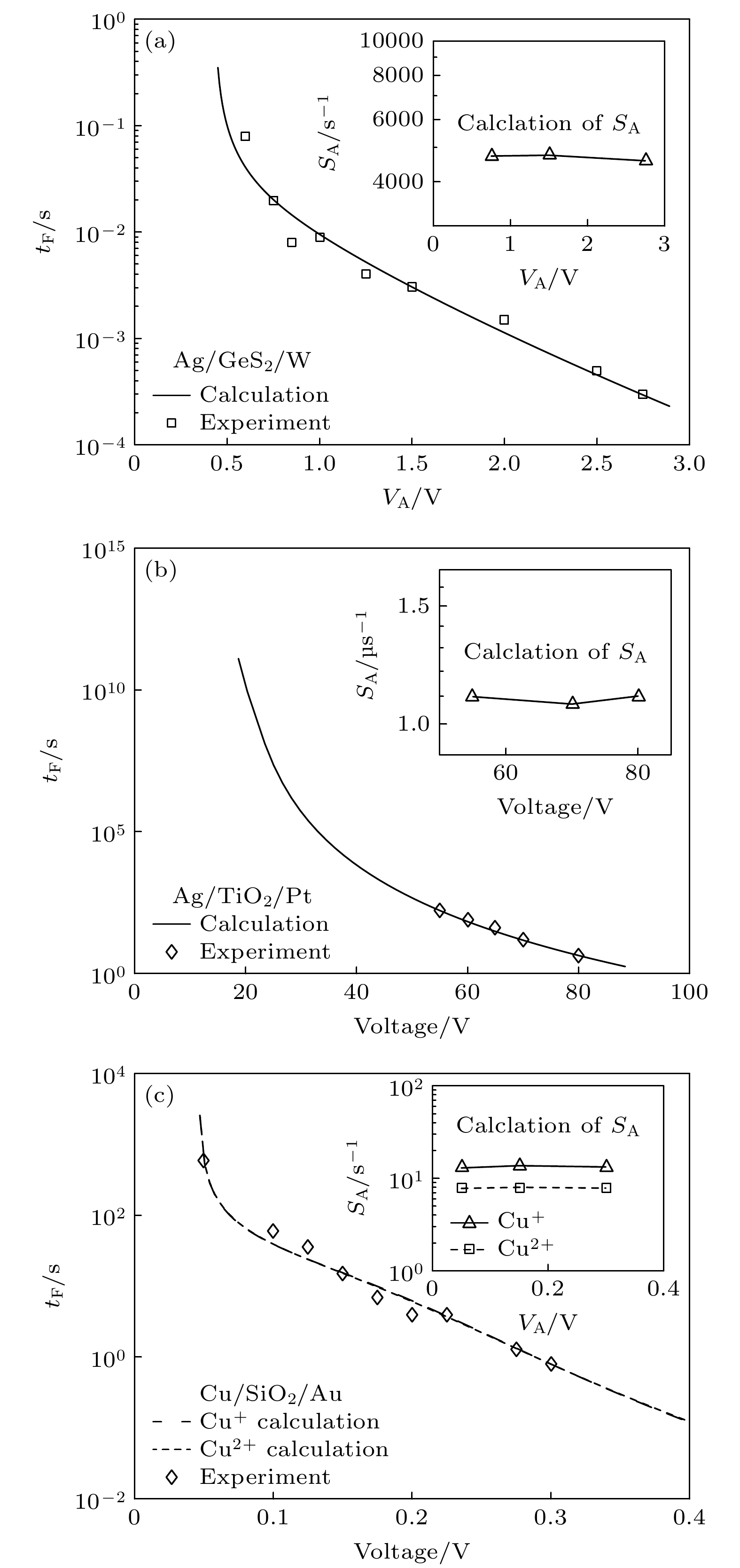
图 5 器件的外加电压与Forming/Set时间(初始导电细丝长度L0 = 0 nm; 图中插图是跃迁速率的计算图) (a) Ag/GeS2/W; (b) Ag/TiO2/Pt; (c) Cu/SiO2/Au
Figure 5. Applied voltage of the device versus the Forming/Set time: (a) Ag/GeS2/W; (b) Ag/TiO2/Pt; (c) Cu/SiO2/Au. The L0 is 0 nm. The inset in the figure is the calculating chart of the jump rate.
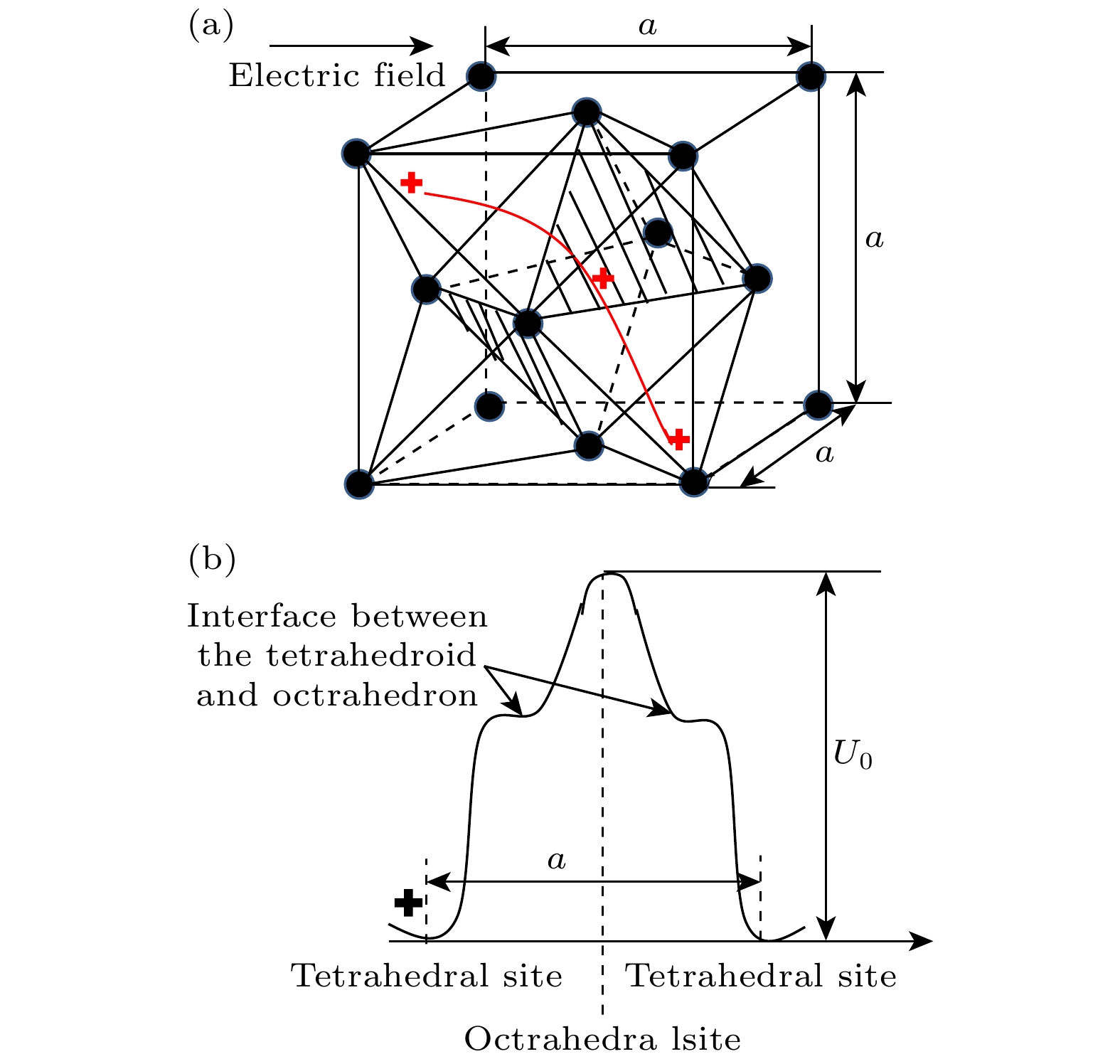
图 6 (a) Ag+离子在γ-AgI中跃迁路径示意图, 红线是离子运动路径, 图中黑球是I–; (b) 离子跃迁遇到的势垒
Figure 6. (a) Schematic diagram of the jump paths for Ag+ in the γ-AgI. The red line is the motion pathway of the cation and the black sphere is the I–. (b) The potential barrier encountered in the process of the ionic jump.

图 7 余弦电势示意图
Figure 7. Schematic diagram of the cosine potential barrier.

图 8 一价离子Ag+和Cu+的参数之间的联系 (a)势垒宽度与激活频率的关系; (b)势垒高度与迁移率的关系
Figure 8. Changes for the parameters of the Ag+ and Cu+: (a) The potential barrier width versus activation frequency; (b) the potential barrier height versus ionic mobility.

图 9 导电细丝生长长度-时间计算结果 (a) Ag/γ-AgI/Pt的细丝生长长度与时间关系; (b) Ag/γ-AgI/Pt的场强与细丝生长长度的关系; (c) Ag/γ-AgI/Pt, Ag/GeS2/W和 Ag/TiO2/Pt细丝生长长度与时间的关系
Figure 9. Relation between the filament growth length versus time in the Ag/γ-AgI/Pt device: (a) Characteristics of the growth length of the conductive filament versus time; (b) schematic diagram of the growth length of the conductive filament versus intensity of the electric field in the Ag/γ-AgI/Pt; (c) schematic diagram of the growth length of the conductive filament versus time in the Ag/γ-AgI/Pt, Ag/GeS2/W, and Ag/TiO2/Pt devices.
表 2 跃迁步长、跃迁速率、阈值电压和σ的计算结果
Table 2. Calculative results of the jump step, jump rate, threshold voltage, and σ
介质 晶胞类型 晶格常数/nm 跃迁步长 as/nm 跃迁速率 SA/s–1 VT/V σ SA 的误差 γ-AgI fcc a = 0.65 0.65 2.0381×10+8 0.2941 0.2769 4.82% TiO2 Rutile a = 0.4594,
c = 0.29560.2956 1.0906×10⁻⁶ 18.5 0.0082 2.78% GeS2 Monoclinic crystal a = 0.672,
b = 1.6101,
c = 1.14361.1436 4.6912×10+3 0.43 0.45 1.75% SiO2
(amorphous)Tetrahedral a = 0.227 0.357 Cu+: 13.3317,
Cu2+: 7.8867Cu+: 0.0461,
Cu2+: 0.0461Cu+: 0.0191,
Cu2+: 0.0398Cu+: 2.97%
Cu2+: 1.60% DownLoad: CSV
表 3 离子在介质中的动力学参数
Table 3. Parameters of ionic kinenics in the dielectric.
电介质 离子 as/nm ν/s–1 U0/eV μion/(cm2·V–1·s–1) Dion/(cm2·s–1) σd/(Ω·cm)–1 γ-AgI Ag+ 0.65 6.3193×10¹¹ 0.1584 3.3119×10⁻⁵ 8.6110×10⁻⁷ 10–5 [13] TiO2 Ag+ 0.2956 3.5913×10¹² 1.0591 3.6652×10⁻²⁰ 9.9257×10⁻²² 2×10–8* [23],
≈10–5** [23]GeS2 Ag+ 1.1436 5.5495×10¹¹ 0.4346 2.3597×10⁻⁹ 6.1352×10⁻¹¹ 1.25×10⁻⁴ [24] SiO2 Cu+ 0.357 2.9321×10¹² 0.6347 6.5350×10⁻¹³ 1.6995×10⁻¹⁴ 1.76×10⁻¹⁵ [25] SiO2 Cu2+ 0.357 2.9643×10¹² 0.6487 7.7319×10⁻¹³ 1.0052×10⁻¹⁴ 1.76×10⁻¹⁵ [25] 注: σd是电介质的电导率, TiO2电导率各向异性, *是垂直c轴的电导率, **是平行c轴的电导率.
DownLoad: CSV
-
[1] Aziza H, Jeremy P P , Bazzi H, Canet P, Moreau M, Marca V D, Harb A T 2020 IEEE Trans. Nanotechnol. 19 214
Google Scholar
[2] Jameson J R, Gilbert N, Koushan F, Wang J, Hollmer S, Kozicki M 2012 Appl. Phys. Lett. 100 023505
Google Scholar
[3] Yu S, Wong P H S 2011 IEEE Trans. Electron. Devices 58 1352
Google Scholar
[4] Hurk J V D, Menzel S, Waser R, Valov I 2015 J. Phys. Chem. C 119 18678
Google Scholar
[5] Covi E, Wang W, Lin Y H, Farronato M, Ambrosi E, Lelmini D 2021 IEEE Trans. Electron. Devices 68 4335
Google Scholar
[6] Valov I, Waser R, Jameson J R, Kozicki M N 2011 Nanotechnology 22 254003
Google Scholar
[7] Lin S, Zhao L, Zhang J Y, Wu H Q, Qian H, Yu Z P 2012 IEEE 2012 International Electron Devices Meeting (IEDM) San Fransisco, USA, December 10−12, 2012 p593
[8] Mott P F, Gurney R W (translated by Pan J S, Li W X) 1953 Electronic Processes in Ionic Crysrals (2nd Ed.) (Bejing: Science Press) p51 (in Chinse) [莫特N F, 格尼R W 著 (潘金声, 李文雄 译) 1959 离子晶体中的电子过程 (北京: 科学出版社) 第51页
Mott P F, Gurney R W (translated by Pan J S, Li W X) 1953 Electronic Processes in Ionic Crysrals (2nd Ed.) (Bejing: Science Press) p51 (in Chinse) [莫特N F, 格尼R W 著 (潘金声, 李文雄 译) 1959 离子晶体中的电子过程 (北京: 科学出版社) 第51页] [9] Zhu J D, Zhang T, Yang Y C, Huang R 2020 Appl. Phys. Rev. 7 011312
Google Scholar
[10] Zhang M Y, Wang G M, Long S B, et al. 2015 IEEE Electron. Device Lett. 36 1303
Google Scholar
[11] Anderson O L, Stuart D A 1954 J. Am. Ceram. Soc. 37 573
Google Scholar
[12] Patnaik J R G, Sunandana C S 1998 J. Phys. Chrn, Solids 59 1059
Google Scholar
[13] Tapperrtzhofen S, Valov I, Waser R 2012 Nanotechnology 23 145703
Google Scholar
[14] Po C, Liao H W, Gan J Y, et al. 2010 ACS Nanotech. 4 5414
Google Scholar
[15] Bermard Y, Gonon P, Jousseaume V 2010 J. Appl. Phys. Lett. 96 193502
Google Scholar
[16] 哈根穆勒P 著 (陈立泉, 薛荣坚 译) 1984 固体电解质一般原理、特征、材料和应用 (北京: 科学出版社) 第29页
Hagenmuller P (translated by Chen L Q, Xue R J) 1984 Solid Electrolytes General Principles, Characterization, Materials, Applications (Bejing: Science Press) p29
[17] Bid A, Bora A, Raychaudhuri A 2006 Phys. Rev. B 74 035426
Google Scholar
[18] Mehrer H 2014 Diffusion in Solids: Fundamentals, Methods, Materials, Diffusion-Controlled Process (New York: Springer Berlin) pp62, 63, 475
[19] 刘明 2018新型阻变存储技术 (北京: 科学出版社) 第88页
Liu M 2018 New Resistive Variable Storage Technology (Beijing: Science Press) p88
[20] 史美仑 1982固体电解质 (重庆: 科学技术文献出版社重庆分社) 第242, 243页
Shi M L 1982 Solid Electrolyte (Chongqing: Chongqing Branch of Science and Technology Literature Press) pp242, 243
[21] Ajayi O B, Nagel L E, Raistrick I D, Huggins R A 1976 J. Phys. Chem. Solids 37 167
Google Scholar
[22] 冯端, 冯晓彤 2005熵的世界 (北京: 科学出版社) 第213页
Feng D, Feng S T 2005 The world of Entropy (Bejing: Science Press) p213
[23] Nowotny M K, Bak T, Nowotny J 2006 J. Phys. Chem. B 110 16271
Google Scholar
[24] Palma G, Vianello E, Cagli C, Molas G, Reyboz M, Blaise P, B. Salvo D, Longnos F, Dahmani F 2012 4th IEEE International Memory Workshop Milan, Italy, May 20−23, 2012 p1
[25] 管绍茂, 王迅 1981半导体表面钝化技术及其应用 (北京: 国防工业出版社) 第70页
Guan S M, Wang X 1981 Semiconductor Surface Passivation Technology and its Application (Bejing: National Defence Industry Press) p70
[26] 哈根穆勒P 著 (陈立泉, 薛荣坚 译) 1984 固体电解质一般原理、特征、材料和应用 (北京: 科学出版社) 第7页
Hagenmuller P (translated by Chen L Q, Xue R J) 1984 Solid Electrolytes General Principles, Characterization, Materials, Applications (Bejing: Science Press) p7
[27] Gao Y R, Adelaide M, Nolan M, Du P, Wu Y F, Yang C, Chen Q L, Mo Y, Bo S H 2020 Chem. Rev. 120 5954
Google Scholar
[28] Shen Z J, Zhao C , Qi Y F, Xu W Y, Liu T, Mitrovic I Z, Yang L, Zhao C 2020 Nanomaterials 10 1437
Google Scholar
[29] Wang W, Covi E K, Lin Y H , Ambrosi E, Milozzi A D, Sbandati C, Farronato M, Ielmini D 2021 IEEE Trans. Electron. Devices 68 4342
Google Scholar
[30] Saadi M, Gonon P, Vallée1 C, Jomni F, Jalaguier E 2020 J. Mater. Sci.-Mater. El. 31 13487
Google Scholar

 DownLoad:
Catalog
Metrics
- Abstract views: 1276
- PDF Downloads: 50
- Cited By: 0
