


-
In van der Waals system, the interlayer van der Waals coupling between adjacent atomically thin layers makes the electronic wave function spread on more than one specific layer, turning spatial discrete layer degree of freedom into a quantum mechanical degree of freedom. The coupling of layer degree of freedom with the in-plane center-of-mass motion of electrons forms a nontrivial layer pseudospin structure in momentum space, resulting in various new quantum geometric properties in an extended parameter space, which is unique to the lattice mismatched van der Waals systems. They trigger off a plenty of novel transport and optical effects, linear and nonlinear responses, and offer new pathways towards device applications, becoming the research frontiers of quantum layertronics. This article briefly reviews this emerging research direction, and discusses possible development in the near future based on its crossing with other intensive research fields such as nonlinear electronics, twistronics and chiral electronics.
-
Keywords:
- quantum layertronics /
- van der Waals systems /
- quantum geometry
[1] Pesin A, MacDonald A H 2012 Nat. Mater. 11 409
 Google Scholar
[2] Xu X D, Yao W, Xiao D, Heinz H T 2014 Nat. Phys. 10 343
Google Scholar
[3] Min H, Borghi G, Polini M, MacDonald A H 2008 Phys. Rev. B 77 041407
Google Scholar
[4] San-Jose P, Prada E, McCann E, Schomerus H 2009 Phys. Rev. Lett. 102 247204
Google Scholar
[5] Banerjee S K, Register L F, Tutuc E, Reddy D, MacDonald A H 2009 IEEE Electron Device Lett. 30 158
Google Scholar
[6] Li S, Gong M, Cheng S, Jiang H, Xie X C 2022 arXiv: 2207.09186
[7] Cullen J H, Bhalla P, Marcellina E, Hamilton A R, Culcer D 2021 Phys. Rev. Lett. 126 256601
Google Scholar
[8] Lesne E, Saǧlam Y G, Battilomo R, Teresa Mercaldo M, van Thiel T C, Filippozzi U, Noce C, Cuoco M, Steele G A, Ortix C, Caviglia A D 2023 Nat. Mater. 22 576
Google Scholar
[9] Liu X, Hsu H C, Liu C X 2013 Phys. Rev. Lett. 111 086802
Google Scholar
[10] Gao A Y, Liu Y F, Hu C W, et al. 2021 Nature 595 521
Google Scholar
[11] Chen R, Sun H P, Gu M, Hua C B, Liu Q, Lu H Z, Xie X C 2022 Natl. Sci. Rev. nwac140
[12] Dai W B, Li H, Xu D H, Chen C Z, Xie X C 2022 Phys. Rev. B 106 245425
Google Scholar
[13] Hanke J P, Freimuth F, Niu C, Blugel S, Mokrousov Y 2017 Nat. Commun. 8 1479
Google Scholar
[14] Xiao C, Xiong B G, Niu Q 2021 Phys. Rev. B 104 064433
Google Scholar
[15] Ma Q, Xu S Y, Shen H T, et al. 2019 Nature 565 337
Google Scholar
[16] Gao A Y, Liu Y F, Qiu J X, et al. 2023 Science 381 181
Google Scholar
[17] Chen C, Zhai D W, Xiao C, Yao W 2023 arXiv: 2303.09973
[18] Matsyshyn O, Xiong Y, Arora A, Song J C W 2023 Phys. Rev. B 107 205306
Google Scholar
[19] Zhai D W, Chen C, Xiao C, Yao W 2023 Nat. Commun. 14 1961
Google Scholar
[20] Andrei E Y, MacDonald A H 2020 Nat. Mater. 19 1265
Google Scholar
[21] Kim C J, Sánchez-Castillo A, Ziegler Z, Ogawa Y, Noguez C, Park J 2016 Nat. Nano 11 520
Google Scholar
[22] Gao Y, Zhang Y H, Xiao D 2020 Phys. Rev. Lett. 124 077401
Google Scholar
[23] Sipe J E, Shkrebtii A I 2000 Phys. Rev. B 61 5337
Google Scholar
[24] Guo C Y, Putzke C, Konyzheva S, Huang X W, Gutierrez-Amigo M, Errea I, Chen D, Vergniory M G, Felser C, Fischer M H, Neupert T, Moll P J W 2022 Nature 611 461
Google Scholar
[25] Zheng H, Zhai D W, Yao W 2022 Nano Lett. 22 5466
Google Scholar
[26] Huang Y X, Feng X L, Wang H, Xiao C, Yang S A 2023 Phys. Rev. Lett. 130 126303
Google Scholar
[27] Yu H Y, Chen M, Yao W 2020 Natl. Sci. Rev. 7 12
Google Scholar
[28] Zhai D W, Yao W 2022 Nat. Sci. 2 e20210101
Google Scholar
[29] Gong Z R, Liu G B, Yu H Y, Xiao D, Cui X D, Xu X D, Yao W 2013 Nat. Commun. 4 2053
Google Scholar
-
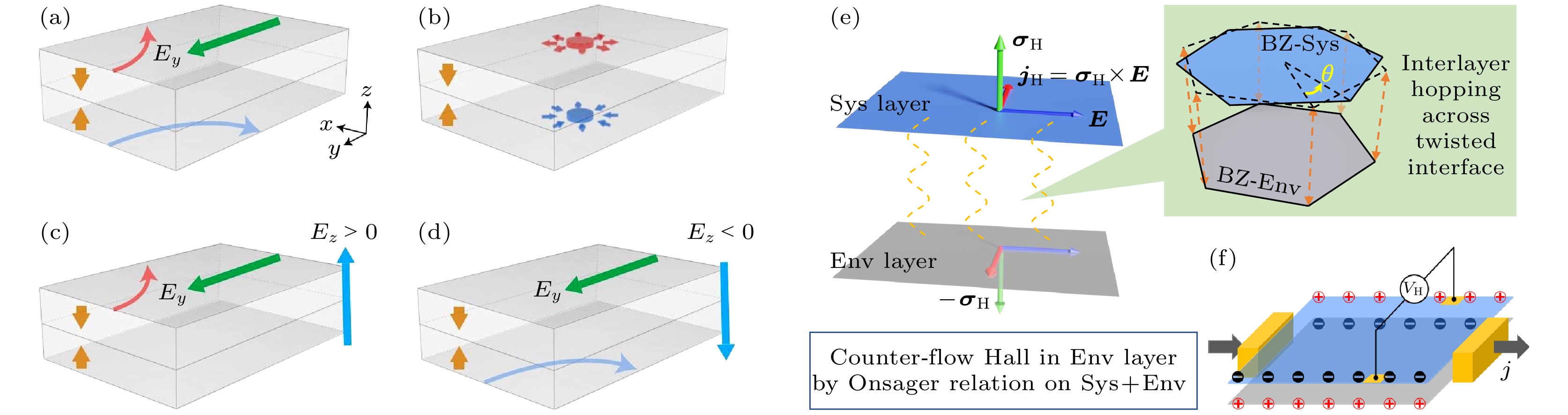
图 1 双层范德瓦耳斯体系中时间反演奇和时间反演偶的线性层霍尔效应 (a)—(d) 双层反铁磁绝缘体中时间反演奇的层霍尔效应, 黄色箭头代表反铁磁自旋构型. (a) 在面内电场 (绿色箭头) 驱动下两层各自有霍尔电流 (红色和蓝色箭头), 大小相等, 方向相反. 这是因为 (b) 两层相反的动量空间贝里曲率 (红色和蓝色箭头). (c), (d) 施加门电场 (蓝绿色箭头) 会使霍尔电流只出现在一层之中, 门电场反向则霍尔电流电流层分布相反. (e), (f) 双层非磁性体系中时间反演偶的层霍尔效应. 红色, 绿色, 蓝色箭头分别代表矢量关系 $ {\boldsymbol{j}}_{{\rm{H}}} $= $ {\boldsymbol{\sigma }}_{{\rm{H}}}\times \boldsymbol{E} $ 中的3个矢量. (e) 非孤立二维系统层 (sys layer, 蓝色平面) 和环境层 (env layer, 灰色平面) 之间的转角界面耦合会在二维非磁性系统层中通过时间反演偶的霍尔效应产生霍尔电流. 而整个双层系统满足的昂萨格关系要求环境层中必然产生相反的霍尔电流. 绿色阴影区域表示两层相对转角为$ \theta $时布里渊区之间的层间跃迁. (f) 样品边界上电荷积累 (红色和黑色, +/–) 导致的时间反演偶的霍尔效应的霍尔电压能够被层分辨的测量所探测, 黑色箭头代表外加驱动电流, 转载自文献 [12, 19]
Figure 1. Time-reversal (TR) odd and even linear layer Hall effects in van der Waals bilayers. (a)–(d) TR odd layer Hall effect in bilayer antiferromagnetic insulators. The yellow arrows denote the antiferromagnetic configuration. (a) The layer Hall counterflow in up and down layers, represented respectively by red and blue arrowed curves, driven by in-plane electric field (green arrow), due to (b) the layer-locked and -contrasted momentum space Berry curvature (the red and blue fluxes); (c), (d) when a perpendicular electric field (the cyan arrow) is applied, the system shows layer-locked anomalous Hall effects tunable by the electric-field direction. (e), (f) TR even layer Hall effect in nonmagnetic van der Waals bilayers. The red, green, and blue arrows denote the three vectors in $ {\boldsymbol{j}}_{{\rm{H}}} $= $ {\boldsymbol{\sigma }}_{{\rm{H}}}\times \boldsymbol{E} $. (e) The twisted interfacial coupling between the system layer (Sys layer, blue plane) and an environmental layer (env layer, gray surface) yields a TR even Hall current in the system layer, whereas a counterflow Hall current is expected in the environmental layer, by Onsager relation on the whole structure: system (Sys) + environment (Env). Green shaded area denotes the interlayer hopping between the Brillouin zone (BZ) with twist angle $ \theta $. (f) The TR-even Hall voltage $ {V}_{{\rm{H}}} $ due to charge accumulation at the sample edges (red and black +/–) can be detected with a layer resolved measurement. Black arrows denote source and drain current $ \boldsymbol{j} $. Reproduced with permission from Refs. [12,19].
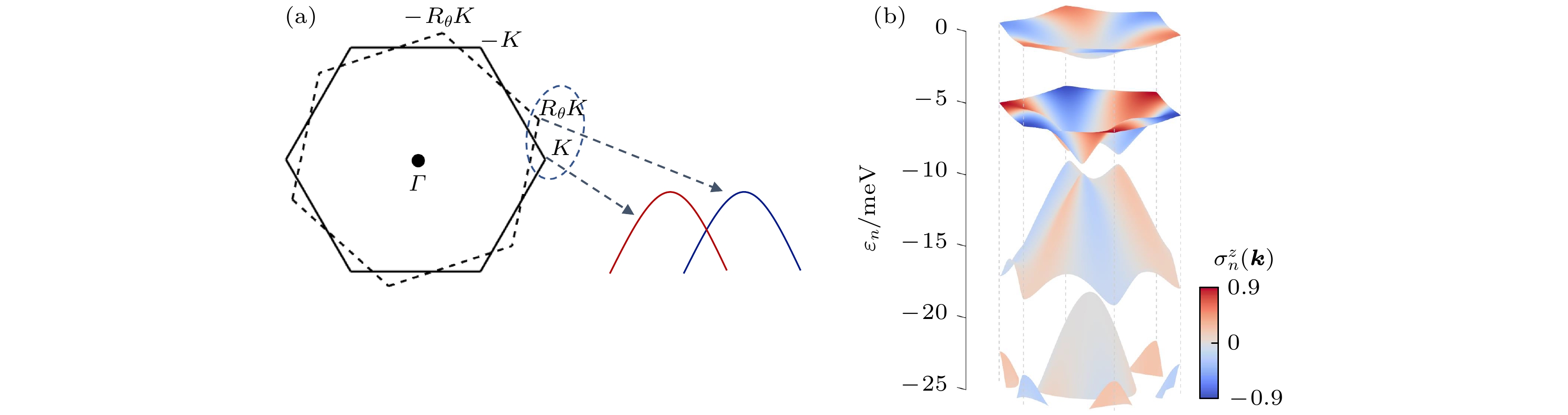
图 2 转角双层过渡金属硫化物体系的超晶格mini能带层赝自旋结构示意图 (a) 两层之间的相对转动导致来自不同层的带边在动量空间中的相对移动 (红色和蓝色曲线分别代表上层和下层的带边色散), 同时也破坏了所有镜面对称性, 导致手征结构; (b) 层间量子隧穿将两层的带边杂化耦合成的mini能带, 图中展示的是2°转角下的能带, 颜色标注$ {\sigma }^{z} $(层赝自旋的z 分量)在超晶格Bloch态下的期待值, 展示了层赝自旋在动量空间的纹理, 由转角调控
Figure 2. Schematics of layer pseudospin structure of twisted bilayer transition metal dichalcogenide: (a) The relative rotation between the two layers leads to the displacement of the degenerate band edges from the two layers (red and blue parabola) in momentum space, and breaks all the mirrors and results in a chiral structure; (b) interlayer quantum tunneling hybridizes the band edges from the two layers and form the superlattice minibands. An example at twisting angle of 2° is shown. Color denotes the expectation value of $ {\sigma }^{z} $, the z component of layer pseudospin, under the superlattice Bloch state, which displaces a layer pseudospin texture that is controlled by twisting angle.
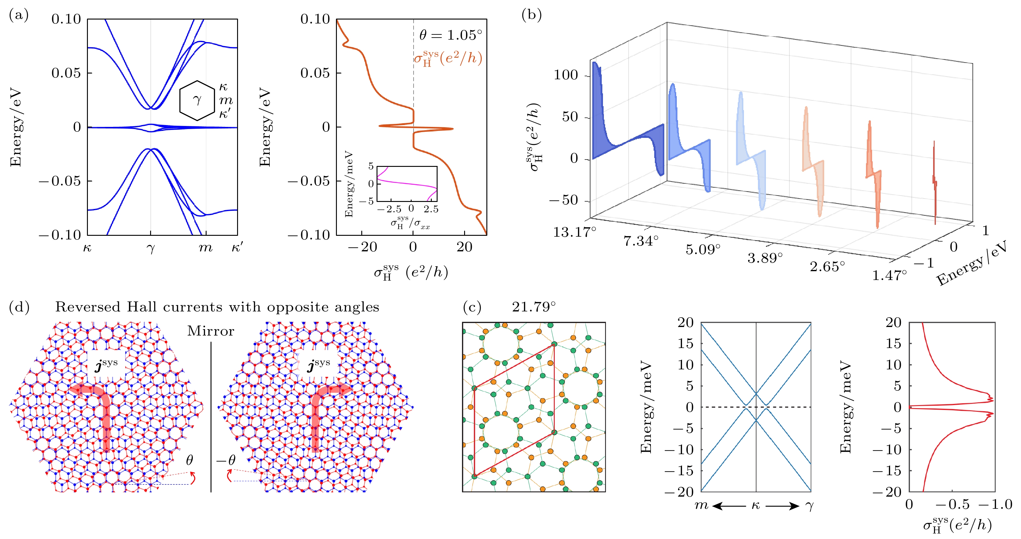
图 3 转角双层石墨烯在不同角度下的能带结构和时间反演偶的霍尔电导率 (a) $ \theta ={1.05}^{\circ}$, 插图描述的是化学势位于中心能带时霍尔电导率 $ {\sigma }_{{\rm{H}}}^{{\rm{s}}{\rm{y}}{\rm{s}}} $ 与纵向电导率 $ {\sigma }_{xx} $ 的比值, 即霍尔比率. (b) 霍尔电导率 $ {\sigma }_{{\rm{H}}}^{{\rm{s}}{\rm{y}}{\rm{s}}} $ 的两个中心峰值随两层石墨烯相对转角的演化. 考虑自旋简并度, 这里霍尔电导率 $ {\sigma }_{{\rm{H}}}^{{\rm{s}}{\rm{y}}{\rm{s}}} $ 要乘以2. (c) 转角 $ \theta ={21.79}^{\circ}$ 时的转角双层石墨烯结构 (红色平行四边形围成的区域是一个莫尔原胞), 狄拉克点附近的低能能带结构, 和系统层中的霍尔电导率. (d) 系统层中的霍尔流 $ {\boldsymbol{j}}^{{\rm{s}}{\rm{y}}{\rm{s}}} $ 会随着两层相对转角变号而反向. 这是因为转角反号后的莫尔体系是反号前体系的镜像对称. 在计算中取电子的弛豫时间为 1 ps. 转载自文献 [19].
Figure 3. Band structure and TR-even Hall conductivity for twisted bilayer graphene at different θ. (a) $ \theta ={1.05}^{\circ}$. Insets: Hall ratio of Hall conductivity $ {\sigma }_{{\rm{H}}}^{{\rm{s}}{\rm{y}}{\rm{s}}} $ to the longitudinal conductivity $ {\sigma }_{xx} $ when the Fermi level is within the central bands. (b) Evolution of the two central peaks of $ {\sigma }_{{\rm{H}}}^{{\rm{s}}{\rm{y}}{\rm{s}}} $ with $ \theta $, here $ {\sigma }_{{\rm{H}}}^{{\rm{s}}{\rm{y}}{\rm{s}}} $ should be multiplied by a factor of 2 accounting for spin degeneracy. (c) Moiŕe of $ \theta ={21.79}^{\circ}$ twisted bilayer graphene (the red lines enclose one unit cell), the low-energy band structure near the Dirac points, and the Hall conductivity in the system layer. (d) Schematics of reversed Hall currents in the system layer $ {\boldsymbol{j}}^{{\rm{s}}{\rm{y}}{\rm{s}}} $ by twisting in opposite directions, where the moiré lattices are mirror images of each other. In the calculations we take the electron relaxation time to be τ = 1 ps. Reproduced with permission from Ref. [19].
-
[1] Pesin A, MacDonald A H 2012 Nat. Mater. 11 409
Google Scholar
[2] Xu X D, Yao W, Xiao D, Heinz H T 2014 Nat. Phys. 10 343
Google Scholar
[3] Min H, Borghi G, Polini M, MacDonald A H 2008 Phys. Rev. B 77 041407
Google Scholar
[4] San-Jose P, Prada E, McCann E, Schomerus H 2009 Phys. Rev. Lett. 102 247204
Google Scholar
[5] Banerjee S K, Register L F, Tutuc E, Reddy D, MacDonald A H 2009 IEEE Electron Device Lett. 30 158
Google Scholar
[6] Li S, Gong M, Cheng S, Jiang H, Xie X C 2022 arXiv: 2207.09186
[7] Cullen J H, Bhalla P, Marcellina E, Hamilton A R, Culcer D 2021 Phys. Rev. Lett. 126 256601
Google Scholar
[8] Lesne E, Saǧlam Y G, Battilomo R, Teresa Mercaldo M, van Thiel T C, Filippozzi U, Noce C, Cuoco M, Steele G A, Ortix C, Caviglia A D 2023 Nat. Mater. 22 576
Google Scholar
[9] Liu X, Hsu H C, Liu C X 2013 Phys. Rev. Lett. 111 086802
Google Scholar
[10] Gao A Y, Liu Y F, Hu C W, et al. 2021 Nature 595 521
Google Scholar
[11] Chen R, Sun H P, Gu M, Hua C B, Liu Q, Lu H Z, Xie X C 2022 Natl. Sci. Rev. nwac140
[12] Dai W B, Li H, Xu D H, Chen C Z, Xie X C 2022 Phys. Rev. B 106 245425
Google Scholar
[13] Hanke J P, Freimuth F, Niu C, Blugel S, Mokrousov Y 2017 Nat. Commun. 8 1479
Google Scholar
[14] Xiao C, Xiong B G, Niu Q 2021 Phys. Rev. B 104 064433
Google Scholar
[15] Ma Q, Xu S Y, Shen H T, et al. 2019 Nature 565 337
Google Scholar
[16] Gao A Y, Liu Y F, Qiu J X, et al. 2023 Science 381 181
Google Scholar
[17] Chen C, Zhai D W, Xiao C, Yao W 2023 arXiv: 2303.09973
[18] Matsyshyn O, Xiong Y, Arora A, Song J C W 2023 Phys. Rev. B 107 205306
Google Scholar
[19] Zhai D W, Chen C, Xiao C, Yao W 2023 Nat. Commun. 14 1961
Google Scholar
[20] Andrei E Y, MacDonald A H 2020 Nat. Mater. 19 1265
Google Scholar
[21] Kim C J, Sánchez-Castillo A, Ziegler Z, Ogawa Y, Noguez C, Park J 2016 Nat. Nano 11 520
Google Scholar
[22] Gao Y, Zhang Y H, Xiao D 2020 Phys. Rev. Lett. 124 077401
Google Scholar
[23] Sipe J E, Shkrebtii A I 2000 Phys. Rev. B 61 5337
Google Scholar
[24] Guo C Y, Putzke C, Konyzheva S, Huang X W, Gutierrez-Amigo M, Errea I, Chen D, Vergniory M G, Felser C, Fischer M H, Neupert T, Moll P J W 2022 Nature 611 461
Google Scholar
[25] Zheng H, Zhai D W, Yao W 2022 Nano Lett. 22 5466
Google Scholar
[26] Huang Y X, Feng X L, Wang H, Xiao C, Yang S A 2023 Phys. Rev. Lett. 130 126303
Google Scholar
[27] Yu H Y, Chen M, Yao W 2020 Natl. Sci. Rev. 7 12
Google Scholar
[28] Zhai D W, Yao W 2022 Nat. Sci. 2 e20210101
Google Scholar
[29] Gong Z R, Liu G B, Yu H Y, Xiao D, Cui X D, Xu X D, Yao W 2013 Nat. Commun. 4 2053
Google Scholar

 DownLoad:
Catalog
Metrics
- Abstract views: 1655
- PDF Downloads: 151
- Cited By: 0
