


-
Metal organic chemical vapor deposition (MOCVD) is a key means of epitaxy of heterojunction semiconductor material, the uniformity of its epitaxial layer thickness will directly affect the yield of the product, especially the vertical cavity surface emitting device, which has a higher requirement for thickness uniformity. For the multi-MO nozzle vertical reaction cavity MOCVD, this paper combines theory and experiment to give an effective method of improving the epitaxial layer thickness uniformity through adjusting the flow rate of each MO nozzle. Firstly, each MO source nozzle is equivalent to an evaporation surface source, and an equivalent height is introduced to cover the relevant epitaxial parameters of MOCVD and the quantitative relationship between the epitaxial layer thickness and the flow rate of each MO source nozzle is established by taking three MO source nozzles as an example. After that, the model parameters are extracted by fitting through the least squares method based on the experimentally measured epitaxial layer thickness distribution results. Finally, based on the extracted model parameters, a method to optimize the epitaxial layer thickness uniformity is given. Accordingly, the AlGaAs resonant cavity structure, which is easy to accurately test the epitaxial layer thickness, is designed and epitaxially grown by using the EMCORE D125 MOCVD system. The statistical results of the mapping reflection spectra of the 4-inch epitaxial wafers are that the average wavelength of the cavity mode is 651.89 nm, with a standard deviation of 1.03 nm, and thickness uniformity of 0.16% is achieved. At the same time, epitaxial growth of GaInP quantum well structure, 4-inch epitaxial wafers mapping photoluminescence spectrum statistics for the average peak wavelength of 653.3 nm, the standard deviation of only 0.46 nm, and peak wavelength uniformity of 0.07% are achieved. Both the wavelength uniformity of cavity mode and the peak wavelength uniformity of quantum well fully meet the requirements of vertical cavity surface emitting device. The method of adjusting epitaxial layer thickness uniformity proposed in this paper is simple, effective, and fast, and it can be further extended to vertical reaction cavity MOCVD systems with more than four MO nozzles.
-
Keywords:
- epitaxial growth /
- least-squares fitting /
- thin-film uniformity /
- metal organic chemical vapor deposition
[1] Manasevit H M 1968 Appl. Phys. Lett. 12 156
 Google Scholar
[2] 陆大成, 段树坤 2009 金属有机化合物气相外延基础及应用 (北京: 科学出版社) 第6页
Lu D C, Duan S K 2009 Fundamentals and Applications of Metal Organic Compound Gas Phase Epitaxy (Beijing: Science Press) p6
[3] Loke W K, Lee K H, Wang Y, Tan C S, Fitzgerald E A, Yoon S F 2018 Semicond. Sci. Technol. 33 115011
Google Scholar
[4] Beckers A, Fahle D, Mauder C, Kruecken T, Boyd A R, Heuken M 2018 SID Symposium Digest of Tecnnical Papers 49 601
Google Scholar
[5] Monge-Bartolome L, Shi B, Lai B, Boissier G, Cerutti L, Rodriguez J B, Lau K M, TourniéE 2021 Opt. Express 29 11268
Google Scholar
[6] Gawron W, Damiecki A, Kozniewski A, Martyniuk P, Stasiewicz K A, Madejczyk P, RutkowskiJ 2021 IEEE Sens. J. 21 4509
Google Scholar
[7] Achilli E, Calicchio M, Armani N, Malvisi E, Annoni F, Cornelli M, Trespidi F, Minuto A, Celi E, Abagnale G, Rizzi S, Timò G 2023 J. Cryst. Growth 607 127131
Google Scholar
[8] 王铄, 王文辉, 吕俊鹏, 倪振华 2021 物理学报 70 026802
Google Scholar
Wang S, Wang W H, Lü J P, Ni Z H 2021 Acta Phys. Sin. 70 026802
Google Scholar
[9] 刘天瑶, 刘灿, 刘开辉 2018 物理学报 71 108103
Google Scholar
Liu T Y, Liu C, Liu K H 2018 Acta Phys. Sin. 71 108103
Google Scholar
[10] 李建军 2018 物理学报 67 067801
Google Scholar
Li J J 2018 Acta Phys. Sin. 67 067801
Google Scholar
[11] 周寅利, 贾雨棽, 张星, 张建伟, 刘占超, 宁永强, 王立军 2022 物理学报 71 134204
Google Scholar
Zhou Y L, Jia Y C, Zhang X, Zhang J W, Liu Z C, Ning Y Q, Wang L J 2022 Acta Phys. Sin. 71 134204
Google Scholar
[12] Manasreh O 2005 Semiconductor Heterojunctions and Nanostructures (New York: The McGraw-Hill Companies, Inc
[13] Heuken M, Krotkus S, Pasko S, Whear O, Wang X, Connan B, McAleese C 2021 ECS Meeting Abstracts MA2021-02 606
Google Scholar
[14] Su J, Armour E, Lee S M, Arif R, Papasouliotis G D 2016 Phys. Status Solidi A 213 856
Google Scholar
[15] Paranjpe A, Montgomery J, Lee S, Morath C 2018 SID Symposium Digest of Technical Papers 49 597
Google Scholar
[16] Chen R, Li J, Ya X, Deng J, Han J, Luo S, Gao L 2010 10th IEEE International Conference on Solid-State and Integrated Circuit Technology Shanghai, China, November 1–4, 2010 pp1853–1855
[17] Zheng W, Li J, Chen R, Yang W, Cui B, Han J, Deng J 2011 International Conference on Remote Sensing, Environment and Transportation Engineering Nanjing, China, June 24–29, 2011 pp5821–5823
[18] Holland L, Steckelmacher W 1952 Vacuum 2 346
Google Scholar
[19] Angus Macleod H 2010 Thin-Film Optical Filters (Fourth Edition) (Balkema: CRC Press) pp598–600
[20] McKee M A, Norris P E, Stall R A, Tompa G S, Chern C S, Noh D, Kang S S, Jasinski T J 1991 J. Cryst. Growth 107 445
Google Scholar
[21] Hartley H O 2012 Technometrics 3 269
Google Scholar
-
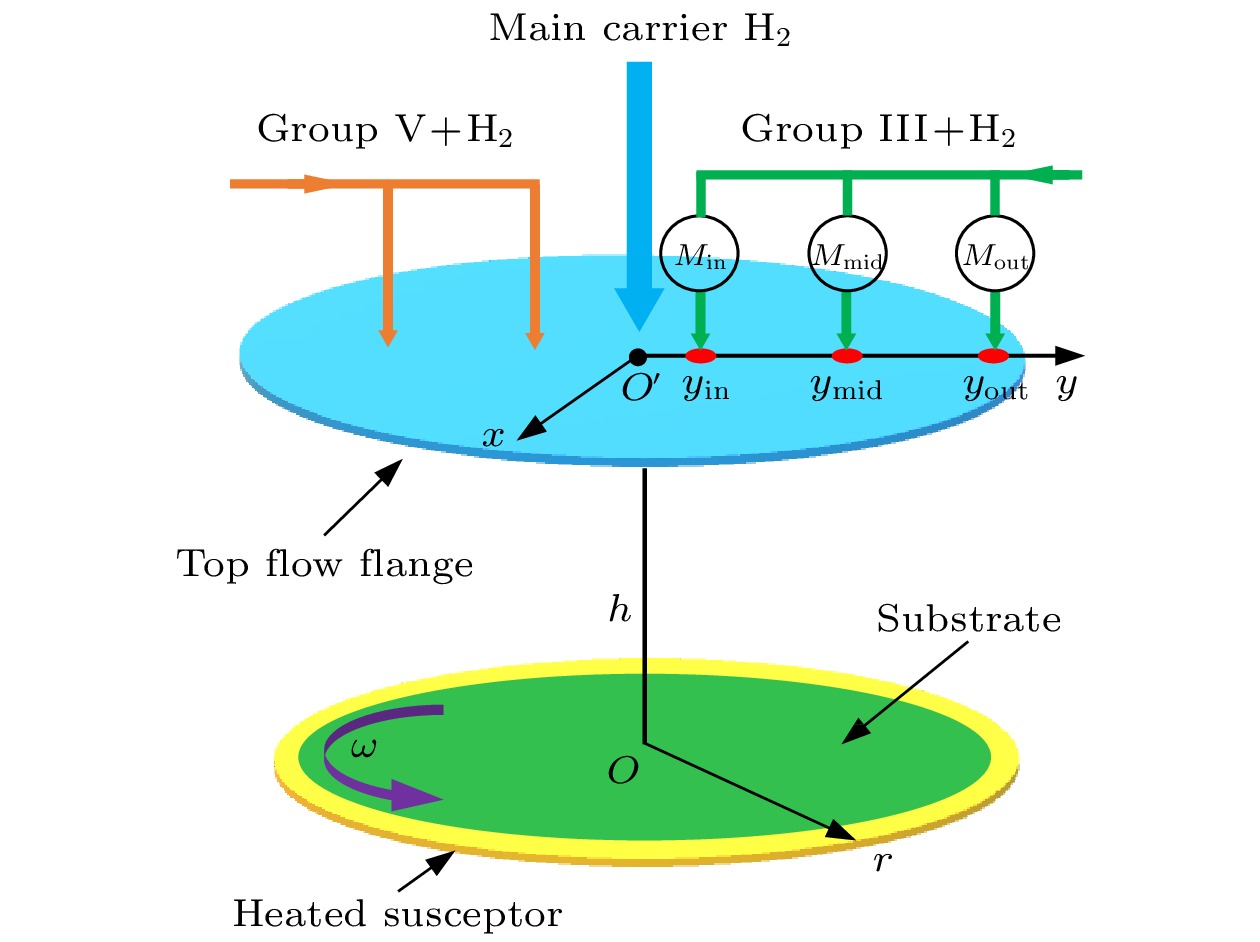
图 1 一种多个Ⅲ族MO喷嘴垂直MOCVD反应腔的简化模型
Figure 1. Simplified chamber model of the vertical MOCVD reactor with multiple group III MO injectors.
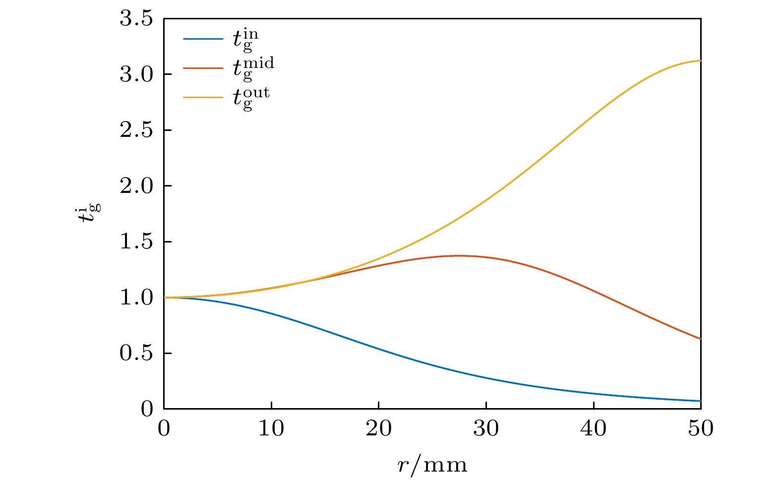
图 2 对应于每个MO喷嘴的相对外延层厚度
Figure 2. Relative epitaxial layer thickness corresponding to each MO injector.
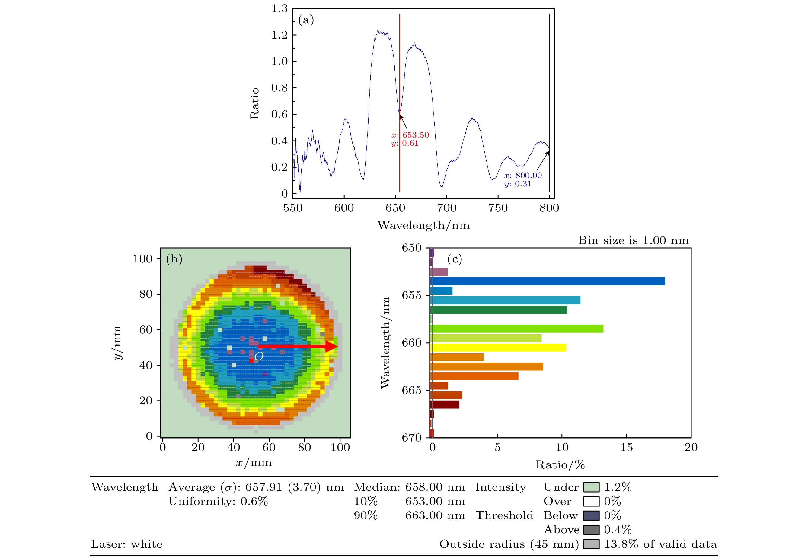
图 3 Bragg cavity#20-2样品的反射谱结果 (a) 外延片中心点的反射光谱; (b) 腔模波长的mapping结果; (c) 整个外延片腔模波长的统计结果
Figure 3. Reflective spectrum results of Bragg cavity#20-2: (a) Reflective spectrum at wafer center point; (b) mapping results of the cavity wavelength; (c) statistic results of the cavity wavelength for the whole wafer.

图 4 Bragg cavty#20-2样品的厚度拟合结果
Figure 4. Thickness fitting results of Bragg cavty#20-2.
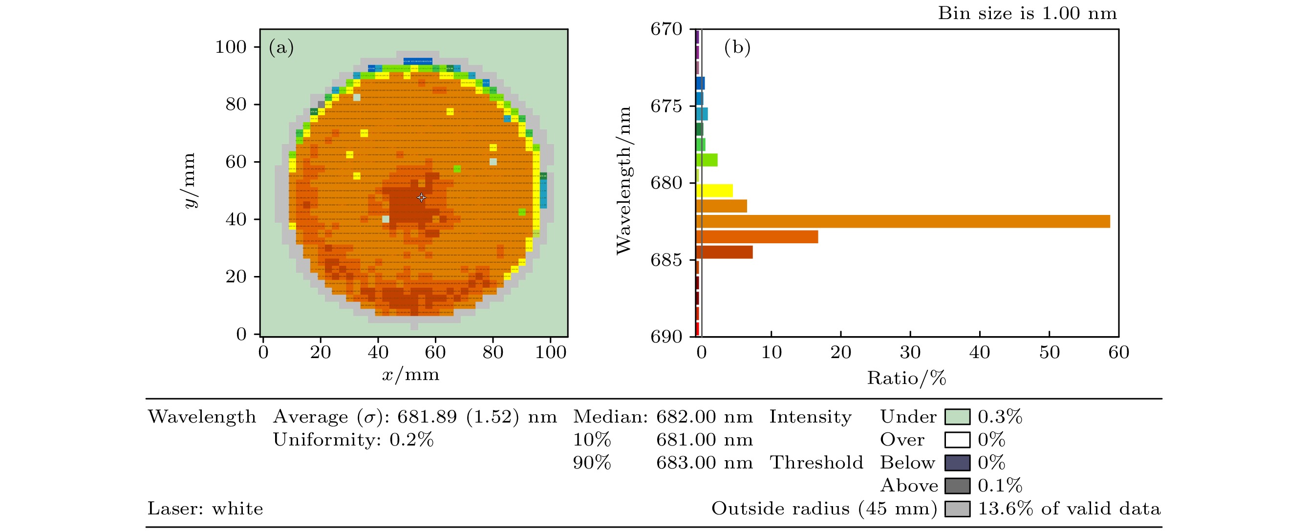
图 5 Bragg cavity#22样品的反射谱结果 (a) 腔模波长的mapping结果; (b) 整个外延片腔模波长的统计结果
Figure 5. Reflective spectrum results of Bragg cavity#22: (a) Mapping results of the cavity wavelength; (b) statistic results of the cavity wavelength for the whole wafer.

图 6 Bragg cavity#23样品的反射谱结果 (a) 腔模波长的mapping结果; (b) 整个外延片腔模波长的统计结果
Figure 6. Reflective spectrum results of Bragg cavity#23: (a) Mapping results of the cavity wavelength; (b) statistic results of the cavity wavelength for the whole wafer.

图 7 650 nm量子阱外延片中心点的PL谱
Figure 7. PL spectrum of 650 nm QW at wafer center point.
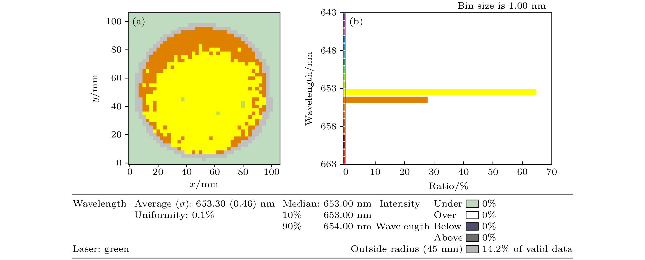
图 8 RCLED QW#69样品的PL谱 (a)峰值波长的mapping结果; (b) 整个外延片峰值波长的统计结果
Figure 8. PL spectrum results of RCLED QW#69: (a) Mapping results of the peak wavelength; (b) statistic results of the peak wavelength for the whole wafer.
表 1 EMCORE D125 MOCVD腔室的结构参数
Table 1. Structure parameters of the EMCORE D125 MOCVD chamber.
yin/mm ymid/mm yout/mm 10 32.5 53  DownLoad: CSV
表 2 用于确定外延层厚度的谐振腔结构
Table 2. Resonant cavity structure to determine the epitaxial layer thickness.
Name 材料 厚度 上DBR 10.5× Al0.95G0.05As 1/4λ Al0.5G0.5As 1/4λ Cavity Al0.95G0.05As 1λ 下DBR 10× Al0.5G0.5As 1/4λ Al0.95G0.05As 1/4λ GaAs substrate
DownLoad: CSV
表 3 典型的外延参数
Table 3. Typical epitaxial parameters.
H2
/sccmAsH3
/sccmV/III
ratio温度
/℃室压
/Pa晶圆载体
转速/(r⋅m–1)20000 100 60—100 600 8000 1000
DownLoad: CSV
表 4 典型的外延参数
Table 4. Typical epitaxial parameters
Bragg
cavity
#20-2Bragg
cavity
#22Bragg
cavity
#23MO源
喷嘴Min/sccm 275.5 281.3 281.3 Mmid/sccm 123.2 125.8 125.8 Mout/sccm 1101.3 1092.9 1092.9 腔模
波长的
mapping
结果$ {\overline{\lambda }}_{{\mathrm{c}}} $/nm 657.9 681.9 651.9 σ/nm 3.7 1.52 1.03 Uniformity/% 0.6 0.2 0.2 λc(10%)/nm 653 681 651 λc(90%)/nm 663 683 653 拟合
结果αin/(nm·sccm–1) 0.891 0.917 0.870 αmid/(nm·sccm–1) 1.868 1.908 1.839 αout/(nm·sccm–1) 0.165 0.174 0.165 heff/mm 30.448 30.748 30.630
DownLoad: CSV
表 5 650 nm量子阱外延结构
Table 5. Epitaxial structure of 650 nm QW.
材料 厚度/nm GaAs 5 (Al0.7G0.3)0.5In0.5P 150 (Al0.5G0.5)0.5In0.5P 35 G0.5In0.5P 5 (Al0.5G0.5)0.5In0.5P ×2 5 G0.5In0.5P ×2 5 (Al0.5G0.5)0.5In0.5P 35 (Al0.7G0.3)0.5In0.5P 150 GaAs substrate
DownLoad: CSV
-
[1] Manasevit H M 1968 Appl. Phys. Lett. 12 156
Google Scholar
[2] 陆大成, 段树坤 2009 金属有机化合物气相外延基础及应用 (北京: 科学出版社) 第6页
Lu D C, Duan S K 2009 Fundamentals and Applications of Metal Organic Compound Gas Phase Epitaxy (Beijing: Science Press) p6
[3] Loke W K, Lee K H, Wang Y, Tan C S, Fitzgerald E A, Yoon S F 2018 Semicond. Sci. Technol. 33 115011
Google Scholar
[4] Beckers A, Fahle D, Mauder C, Kruecken T, Boyd A R, Heuken M 2018 SID Symposium Digest of Tecnnical Papers 49 601
Google Scholar
[5] Monge-Bartolome L, Shi B, Lai B, Boissier G, Cerutti L, Rodriguez J B, Lau K M, TourniéE 2021 Opt. Express 29 11268
Google Scholar
[6] Gawron W, Damiecki A, Kozniewski A, Martyniuk P, Stasiewicz K A, Madejczyk P, RutkowskiJ 2021 IEEE Sens. J. 21 4509
Google Scholar
[7] Achilli E, Calicchio M, Armani N, Malvisi E, Annoni F, Cornelli M, Trespidi F, Minuto A, Celi E, Abagnale G, Rizzi S, Timò G 2023 J. Cryst. Growth 607 127131
Google Scholar
[8] 王铄, 王文辉, 吕俊鹏, 倪振华 2021 物理学报 70 026802
Google Scholar
Wang S, Wang W H, Lü J P, Ni Z H 2021 Acta Phys. Sin. 70 026802
Google Scholar
[9] 刘天瑶, 刘灿, 刘开辉 2018 物理学报 71 108103
Google Scholar
Liu T Y, Liu C, Liu K H 2018 Acta Phys. Sin. 71 108103
Google Scholar
[10] 李建军 2018 物理学报 67 067801
Google Scholar
Li J J 2018 Acta Phys. Sin. 67 067801
Google Scholar
[11] 周寅利, 贾雨棽, 张星, 张建伟, 刘占超, 宁永强, 王立军 2022 物理学报 71 134204
Google Scholar
Zhou Y L, Jia Y C, Zhang X, Zhang J W, Liu Z C, Ning Y Q, Wang L J 2022 Acta Phys. Sin. 71 134204
Google Scholar
[12] Manasreh O 2005 Semiconductor Heterojunctions and Nanostructures (New York: The McGraw-Hill Companies, Inc
[13] Heuken M, Krotkus S, Pasko S, Whear O, Wang X, Connan B, McAleese C 2021 ECS Meeting Abstracts MA2021-02 606
Google Scholar
[14] Su J, Armour E, Lee S M, Arif R, Papasouliotis G D 2016 Phys. Status Solidi A 213 856
Google Scholar
[15] Paranjpe A, Montgomery J, Lee S, Morath C 2018 SID Symposium Digest of Technical Papers 49 597
Google Scholar
[16] Chen R, Li J, Ya X, Deng J, Han J, Luo S, Gao L 2010 10th IEEE International Conference on Solid-State and Integrated Circuit Technology Shanghai, China, November 1–4, 2010 pp1853–1855
[17] Zheng W, Li J, Chen R, Yang W, Cui B, Han J, Deng J 2011 International Conference on Remote Sensing, Environment and Transportation Engineering Nanjing, China, June 24–29, 2011 pp5821–5823
[18] Holland L, Steckelmacher W 1952 Vacuum 2 346
Google Scholar
[19] Angus Macleod H 2010 Thin-Film Optical Filters (Fourth Edition) (Balkema: CRC Press) pp598–600
[20] McKee M A, Norris P E, Stall R A, Tompa G S, Chern C S, Noh D, Kang S S, Jasinski T J 1991 J. Cryst. Growth 107 445
Google Scholar
[21] Hartley H O 2012 Technometrics 3 269
Google Scholar

 DownLoad:
Catalog
Metrics
- Abstract views: 652
- PDF Downloads: 19
- Cited By: 0
