


Scalable production of two-dimensional materials
自 2004年石墨烯被首次从石墨中解理出来以来, 二维材料的研究已经走过了 18个年头. 在这近二十年的时间里, 二维材料已经发展成为一个庞大的家族; 这些二维材料展现出丰富多样的性质,涵盖了凝聚态物理研究的各个主要方向. 更为重要的是, 二维材料研究开辟了一个材料物理研究的新范式: 把一个层状的晶体块材减薄到单层或少层, 所得到的二维材料往往会展现出与块材母体完全不一样的特性. 新的物理也随之涌现, 例如石墨烯中的狄拉克费米子物理以及单层二维过渡金属硫族化合物中的谷自旋物理. 更进一步, 这些二维材料原则上可以像魔角双层石墨烯一样, 通过堆叠形成异质结, 成为发现新效应、新物理的另一个源泉. Mounet等人的计算表明, 迄今实验上制备出的二维材料只是冰山的一角, 理论上可以解理到单层的二维材料可能有上千种. 二维材料及其异质结构的研究因此蕴含着巨大的原创性发现的机会.
在所有这些二维材料中, 原子在层内都是通过共价键和离子键等强化学键结合在一起, 同时面外的化学键呈饱和状态, 层与层之间仅以弱范德华力相结合. 这个结构上的共性保证了二维材料即使在单层极限下也可以保有其结构的完整性和化学的稳定性. “界面即器件”, 二维材料本身就是一个界面, 基于二维材料的半导体器件电场对沟道的调控更彻底, 从而抑制纳米尺度下半导体器件中的短沟道效应. 在器件尺寸已经微缩到纳米量级的后摩尔时代, 以过渡金属硫族化合物、黑磷为代表的二维材料在极限厚度下表现出优异的半导体特性, 作为未来半导体器件沟道的候选材料受到广泛关注. 与此同时, 二维材料单层极限下的化学稳定性也使得更多样的调控手段成为可能. 比如, 近年来日益受到重视的门电极离子调控可以在 1014cm–2的水平调控二维材料的电荷掺杂, 从而把门电极调控的概念推广到磁性、强关联乃至高温超导材料. 基于这些新型调控方法的二维器件将有可能发展为新的器件原型.
从二维材料到器件再到应用, 这个链条上不可或缺的一环是二维材料的宏观制备——只有在宏观尺度下实现高质量二维材料的可控制备, 我们以上讨论的二维材料的种种优势才有可能转化为实际的应用. 正因如此, 二维材料的宏观制备一直是二维材料研究的一个热点和前沿, 近年来取得了一个又一个的突破. 这些突破有许多要归功于海内外的华人物理、材料学家. 他们活跃在这个前沿,做出了突出的成绩.
受《物理学报》编辑部委托, 我邀请了几位活跃在二维材料宏观制备研究前沿的中青年学者,为中文读者回顾总结领域里近年来的部分进展. 其中既包括对多种二维材料自下而上的生长研究,也包括从块材出发自上而下的大面积解理探索. 组稿期间恰逢新冠疫情肆虐, 作者们在非常困难的情形之中完成稿件, 如约赐稿, 殊为不易. 受水平及时间所限, 本专题对二维材料宏观制备领域的介绍难免挂一漏万, 不足之处恳请各位同仁不吝指正.
2022, 71 (10): 108103.
doi: 10.7498/aps.71.20212399
Abstract +
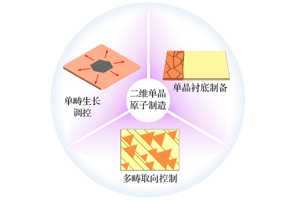
With the shrinkage of the chip feature size, the short-channel effect becomes more and more predominate. The development of new quantum materials for high-performance devices has become imperative for the current technological development. Two-dimensional (2D) materials, due to their excellent physical and chemical properties, are thought to be the promising candidate of quantum materials for achieving the high-end electronic and optoelectronic devices. Like the development of silicon-based chips, the wafer-scale device applications of 2D materials must be based on the fabrication of high-quality, large-size 2D single crystals. However, the existing manufacturing techniques of the well-studied bulk single crystals cannot be fully applied to the fabrication of 2D single crystals due to the interfacial characteristics of 2D materials. So far, single crystals of metre-sized graphene, decimetre-sized hBN and wafer-sized TMDCs have been successfully prepared by chemical vapor deposition, but the sizes of other 2D single crystals are still very limited and not in the same league as conventional semiconductor materials. Therefore, it is urgent to develop an effective preparation strategy for the manufacture of various 2D single crystals. In this review, we mainly overview the fabrication techniques for the meter-scale growth of 2D single crystals, and propose three key modulation aspects in the atomic-scale manufacture, i.e. the growth modulation of 2D single nucleus, the preparation of single-crystal substrates, and the alignment control of 2D single-crystal domains, in order to provide a universal method of fabricating the large-size 2D single crystals. Finally, the prospect of chip devices based on these high-quality large-size novel 2D single crystals is discussed, thereby paving the way for the future industrial applications of electronics and optoelectronics.

2022, 71 (10): 106801.
doi: 10.7498/aps.71.20212407
Abstract +
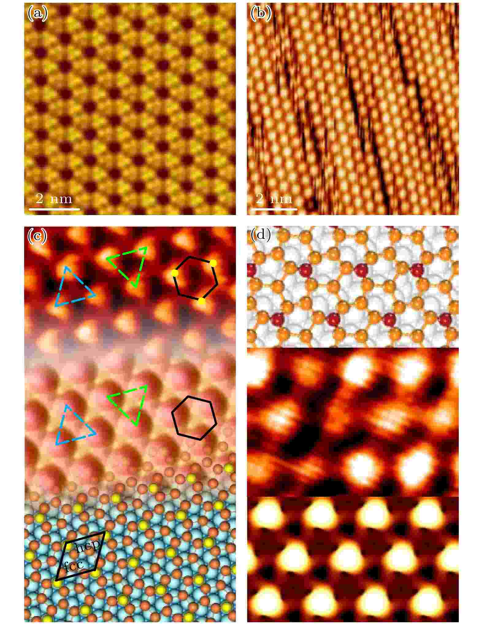
Compared with the three-dimensional bulk materials, two-dimensional (2D) materials exhibit superior electronic, optical, thermal, and mechanical properties due to the reduced dimensionality. The quantum confinement effect of 2D materials gives rise to exotic physical properties, and receives extensive attention of the scientists. Lots of routes to fabricate the 2D materials have been proposed by the material scientists, including the traditional mechanical exfoliation, chemical vapor deposition, molecular beam epitaxy under ultra-high vacuum (UHV), and so on. Among them, fabricating materials under ultra-high vacuum has the advantages of constructing large-scale and high-quality samples, and is therefore widely adopted in the 2D material growth. In this paper, we review three different strategies of growing 2D materials under UHV conditions, including molecular beam epitaxy, graphene intercalation and manual manipulation by nano probes. We compare the advantages and drawbacks among those methods in creating 2D materials, and try to provide some guidance to the community, especially those who are new to the field.
2022, 71 (10): 108104.
doi: 10.7498/aps.71.20220155
Abstract +
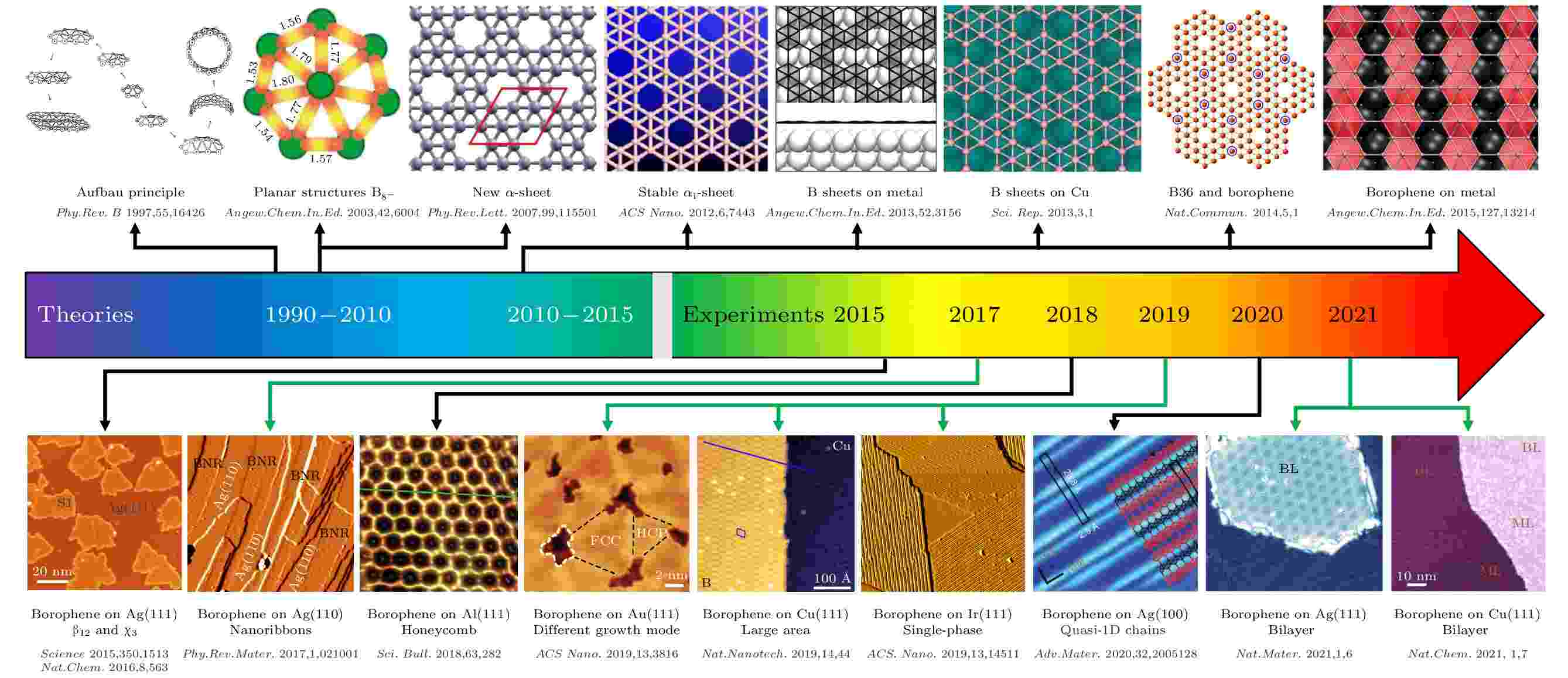
As the lightest two-dimensional material discovered so far, borophene exhibits rich physical properties, including high flexibility, optical transparency, high thermal conductivity, one-dimensional nearly free electron gas, Dirac fermions, and superconductivity. However, due to the strong interlayer covalent bonding force of bulk boron, it is difficult to obtain the monolayer borophene via mechanical exfoliation. In addition, due to the electron-deficient property of boron atoms, its chemical properties are relatively active, and its bonding is complex, resulting in different boron allotropes, which is different from other two-dimensional materials. For a long time, the research on borophene has been limited to theoretical exploration, and it has been difficult to make breakthroughs in the experimental synthesis of two-dimensional borophene. It has been only successfully prepared by a few research groups in recent years. However, there is still huge space for exploration on the growth, structure and electronic properties of borophene. This paper systematically reviews the preparation methods and different structures of borophene under different substrates, and its growth mechanism is discussed. It provides a research platform for further expanding the physical properties of borophene, and provides ideas for exploring the preparation of borophene nanodevices. It has great potential application prospects in high energy storage, optoelectronic devices, high detection sensitivity, and flexible nanodevices.

2022, 71 (10): 108102.
doi: 10.7498/aps.71.20212447
Abstract +
Monolayer molybdenum disulfide (MoS2) is an emerging two-dimensional (2D) semiconductor material.The MoS2 film has a natural atomic-level thickness, excellent optoelectronic and mechanical properties, and it also has the potential applications in very large-scale integration technology in the future. In this article we summarize the research progress made by our group in the studying of monolayer MoS2 films in the past few years. The controlled growth of large-size MoS2 single crystals is achieved by oxygen-assisted chemical vapor deposition method. By a unique facile multisource CVD growth method, the highly oriented and large domain size ML MoS2 films are epitaxially grown on a 4-inch wafer scale. Almost only 0° and 60° oriented domains are present in films, and the average size of MoS2 grains ranges from 100 μm to 180 μm . The samples exhibit their best optical and electrical quality ever obtained, as evidenced from their wafer-scale homogeneity, nearly perfect lattice structure, average room-temperature device mobility of ~70 cm2·V–1·s–1 and high on/off ratio of ~109 on SiO2 substrates. By adjusting the oxygen doping concentration in the MoS2 film through using an effective CVD technique, electrical and optical properties can be well modified, thereby greatly improving the carrier mobilities and controllable n-type electronic doping effects resulting from optimized oxygen doping levels of MoS2–xOx . In terms of MoS2 thin film devices and applications, the 4-inch wafer-scale high-quality MoS2 monolayers are used to fabricate the transparent MoS2-based transistors and logic circuits on flexible substrates. This large-area flexible FET device shows excellent electrical performance with a high device density (1,518 transistors per cm2) and yield (97%), and exhibits a high on/off ratio (1010), current density (~35 μA·μm–1), mobility (~55 cm2·V–1·s–1) and flexibility. Based on the vertically integrated multilayer device via a layer-by-layer stacking process, an individual layer of all-2D multifunctional FET is successfully achieved with nearly multiplied on-current density, equivalent device mobility, and persevered on/off ratio and subthreshold swing (SS) of the individual layer, the combined performance of the device is fully utilized, and the integration of “sensing-storing-computing” is realized. A two-terminal floating-gate memory (2TFGM) based artificial synapse built from all-2D van der Waals materials is prepared, the 2TFGM synaptic device exhibits excellent linear and symmetric weight update characteristics with high reliability and tunability. A large number of states of up to ≈3000, high switching speed of 40 ns and low energy consumption of 18 fJ for a single pulse are demonstrated experimentally. The introduction of structural domain boundaries in the basal plane of monolayer MoS2 can greatly enhance its hydrogen evolution reaction performance by serving as active sites. The progress we have made in the preparation of monolayer MoS2 films and the research on device characteristics is of guiding significance for the basic and application research of MoS2, and also is universal and instructive for other 2D transition metal dichalcogenides.

2022, 71 (10): 108201.
doi: 10.7498/aps.71.20220030
Abstract +
Since the monolayer graphene was first obtained in the year of 2004, mechanical exfoliation technique has been widely used to prepare various two-dimensional materials such as transition metal dichalcogenides and black phosphorus. Among a variety of preparation techniques of two-dimensional materials, mechanical exfoliation technique shows advantages in its simplicity and universality. More importantly, the exfoliated two-dimensional samples are the ideal ones for many novel phenomena. This paper introduces the background of mechanical exfoliation technique and summarizes the problems of conventional mechanical exfoliation technique in the development of two-dimensional materials. In order to solve the problems of low efficiency and small sample size of conventional mechanical exfoliation technique, some modified mechanical exfoliation techniques have been developed, such as oxygen-plasma-assisted exfoliation method and gold-film-assisted exfoliation method. As a commonly used “top-down” preparation method, the new exfoliation technology is still full of vitality in basic research and application of two-dimensional materials. In the future, larger size and higher quality will be the development direction of exfoliation technology.
2022, 71 (16): 166101.
doi: 10.7498/aps.71.20220388
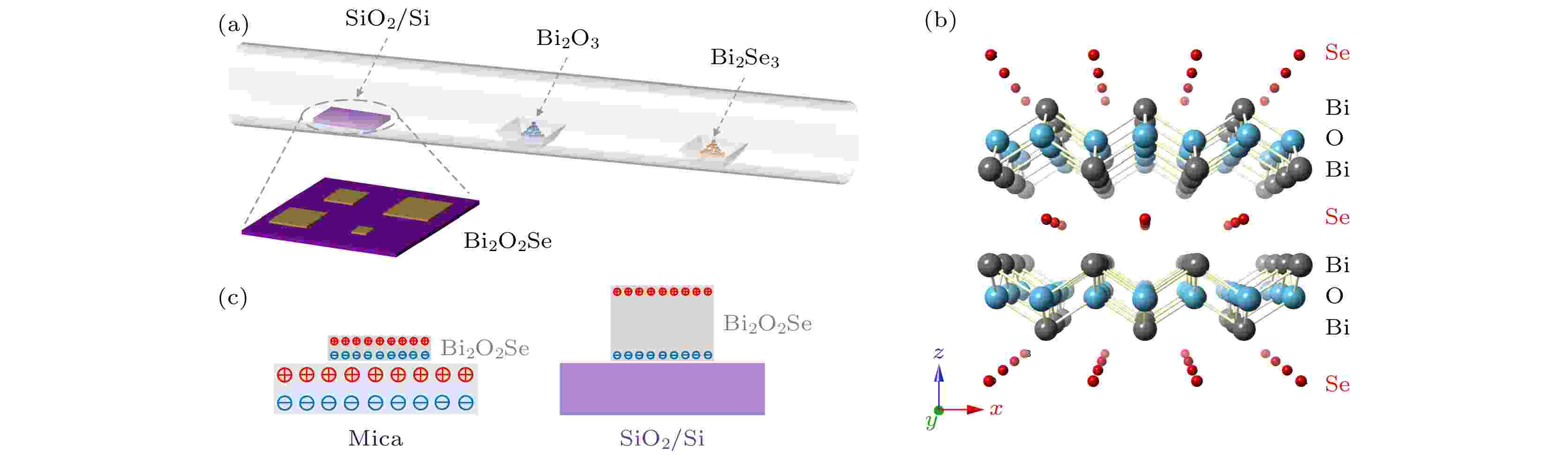
Abstract +
As the scaling-down of semiconductor processing technology goes on, it is urgent to find the successor of silicon-based materials since the severe short channel effect lowers down their energy efficiency as logic devices. Owing to its atomic thickness and van der Waals surface, two-dimensional semiconductors have received huge attention in this area, among which Bi2O2Se has achieved a good trade-off among the carrier mobility, stability and costing. However, the synthesis of Bi2O2Se need some polarized substrates, which hinders its processing and application. Here, a Bi2O2Se layer with 25 µm in size and 51.0 nm in thickness is directly synthesized on a silicon substrate via chemical vapor deposition . A Field-effect transistor with a carrier mobility of 80.0 cm2/(V·s) and phototransistor with a photoresponsivity of 2.45×10⁴ A/W and a photogain of 6×10⁴ is also demonstrated, which hpossesses quite outstanding photodetection performance. Nevertheless, the high dark current and low on/off ratio brought by the large thickness leads to a fair detectivity (5×10¹⁰ Jones). All in all, , although silicon substrate brings convenience in device fabricating, it is still needed to further optimizing the growth and integrating more applications of various two-dimensional materials .
