


-
The second harmonic generation (SHG), as a nonlinear optical effect, has a wide range of applications in obtaining information such as material composition, structure, and properties due to its good polarization sensitivity. Although SHG spectroscopy or SHG microscopy has been used to explore the precise positioning or tracking of nanowires, there are few reports on the combination of SHG spectroscopy and SHG microscopy to study the structure of nanomaterials and the spatial orientation of crystal axes. In this work, we investigate the spatial orientation and crystal axis orientation of cadmium sulfide (CdS) nanowires by combining SHG spectroscopy and microscopic imaging. Firstly, we experimentally and theoretically study the spectral intensity of the SHG of CdS nanowires with the polarization direction of the incident light based on the all-optical analysis method proposed by the predecessors. We also analyze the influence of the azimuth angle of the crystal axis γ, ω and φ on the pattern of the SHG of CdS nanowires in detail. Secondly, through the mutual verification of theoretical calculations and experimental measurement results, we successfully determine the three axial orientations of a single CdS nanowire. Finally, we also investigate the spatial orientation of a single CdS nanowire by using the polarization-dependent SHG microscopic imaging method. It is shown that different parts of the CdS nanowire have different SHG responses when the polarization is changed. These results provide a new idea and an important reference for studying the application of SHG spectroscopy and microscopic imaging in the research of high-precision spatial positioning of nanomaterials. This study provides important enlightenment for realizing the potential applications of nanomaterials in biomedicine.
-
Keywords:
- second harmonic generation /
- CdS nanowire /
- polarization /
- crystal orientation
[1] 白瑞雪, 杨珏晗, 魏大海, 魏钟鸣 2020 物理学报 69 184211
 Google Scholar
Bai R X, Yang Y H, Wei D H, Wei Z M 2020 Acta Phys. Sin. 69 184211
Google Scholar
[2] Fan X, Zhang M L, Shafiq I, Zhang W J, Lee C S, Lee S T 2009 Cryst. Growth Des. 9 1375
Google Scholar
[3] Lin Y F, Song J, Ding Y, Lu S Y, Zhang Z L 2008 Adv. Mater. 20 3127
Google Scholar
[4] Zhai T Y, Gu Z J, Zhong H Z, Dong Y, Ma Y, Fu H B, Li Y F, Yao J N 2007 Cryst. Growth Des. 7 488
Google Scholar
[5] Lin Y F, Song J, Ding Y, Lu S Y, Zhang Z L 2008 Appl. Phys. Lett. 92 022105
Google Scholar
[6] Zhai T Y, Fang X S, Li L, Bando Y, Golberg D 2010 Nanoscale 2 168
Google Scholar
[7] Ma R M, Wei X L, Dai L, Dai L, Huo H B, Qin G G 2007 Nanotechnology 18 205605
Google Scholar
[8] Li H Q, Wang X, Xu J Q, Zhang Q, Bando Y, Golberg D 2013 Adv. Mater. 25 3017
Google Scholar
[9] Nakayama Y, Pauzauskie P, Radenovic A, Onorato R M, Saykally R J, Liphardt J, Yang P D 2007 Nature 447 1098
Google Scholar
[10] Prasanth R, van Vugt L K, Vanmaekelbergh D A M, Gerritsen H C 2006 Appl. Phys. Lett. 88 181501
Google Scholar
[11] Tian B Z, Zheng X L, Kempa T J, Fang Y, Yu N F, Yu G H, Huang J L, Lieber C M 2007 Nature 449 885
Google Scholar
[12] Allen J E, Hemesath E R, Perea D E, Lensch-Falk J L, Liz Y, Yin F, Gass M H, Wang P, Bleloch A L, Palmer R E, Lauhon L J 2008 Nat. Nanotechnol. 3 168
Google Scholar
[13] Mu S, Chang J C, Lee S T 2008 Nano Lett. 8 104
Google Scholar
[14] Peng K Q, Wang X, Wu X L, Lee S T 2009 Nano Lett. 9 3704
Google Scholar
[15] Nadia M J, Nada H 2018 International Conference on Materials Engineering and Science Istanbul Turkey, August 8–11, 2018 p012111
[16] Hu H B, Wang K, Long H, Liu W W, Wang B, Lu P X 2015 Nano Lett. 15 3351
Google Scholar
[17] Bautista G, Makitalo J, Chen Ya, Dhaka V, Grasso M, Karvonen L, Jiang H, Huttunen M J, Huhtio T, Lipsanen H, Kauranen M 2015 Nano Lett. 15 1564
Google Scholar
[18] Kim W, Ng J K, Kunitake M E, Conklin B R, Yang P D 2007 J. Am. Chem. Soc. 129 7728
Google Scholar
[19] Jung Y, Tong L, Tanaudommongkon A, Cheng J X, Yang C 2009 Nano Lett. 9 2440
Google Scholar
[20] Xu J Y, Rechav K, Popovitz-Biro R, Nevo I, Feldman Y, Joselevich E 2018 Adv. Mater. 30 1800413
Google Scholar
[21] Wang J J, Zhang X, Deng J B, Hu X, Hu Y, Mao J, Ma M, Gao Y H, Wei Y C, Li F, Wang Z H, Liu X L, Xu J Y, Ren L Q 2021 Molecules 26 5178
Google Scholar
[22] Shoji I, Kondo T, Ito R 2002 Opt. Quant. Electron. 34 797
Google Scholar
-
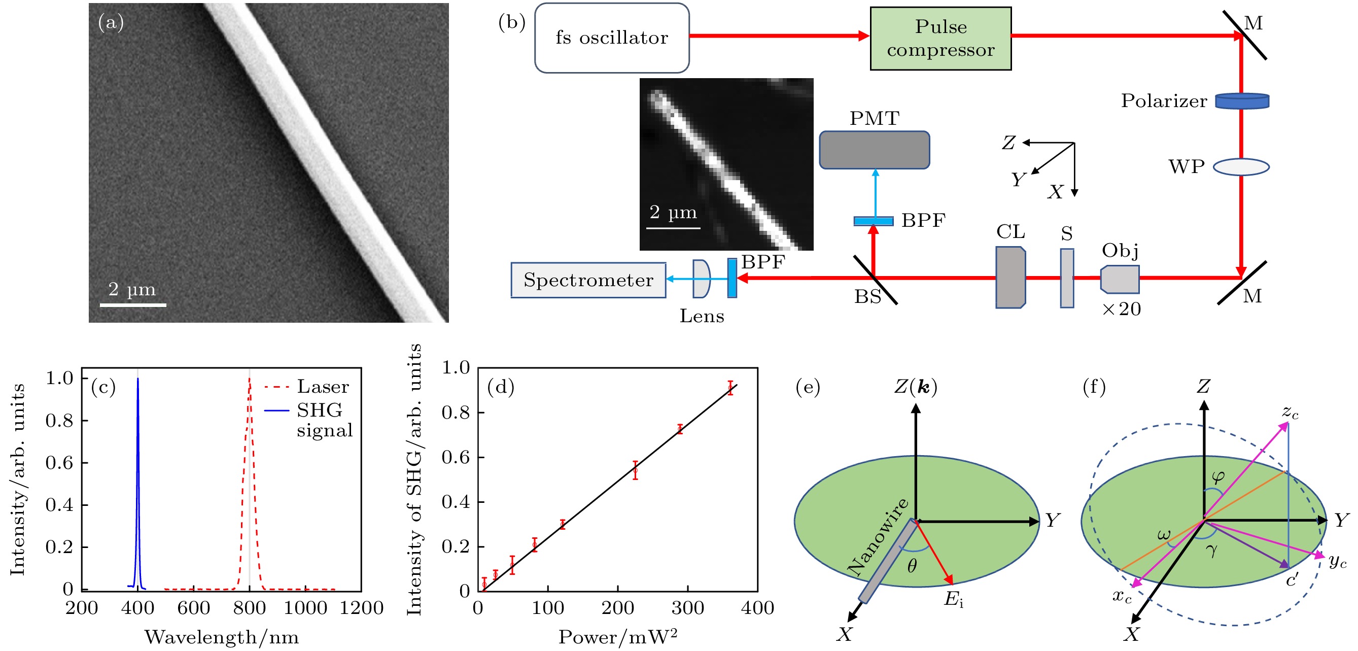
图 1 单根CdS纳米线的SHG实验装置与测量结果研究 (a) 化学气相沉积法生长的单根CdS纳米线SEM图; (b) SHG光谱与显微成像装置及CdS纳米线的SHG显微成像图; (c) 归一化处理的激光光谱(红色虚线)与SHG光谱(蓝色实线); (d) SHG信号强度和激发光强度平方之间的关系图; 测量误差也显示在图中; (e) 实验室框架的几何形状(XYZ), 线偏振泵浦激光沿Z轴传输. 泵浦激光的光电场Ei在XY平面内, 与纳米线生长轴成可变角度θ; (f) 晶体框架(xcyczc)在实验室框架中的相对位置; φ是zc和Z轴之间的夹角, γ是X轴和zc在xy平面上的投影($ c' $)之间的夹角, ω是xc和XY平面和xcyc平面的交线之间的夹角, 晶体zc的取向与CdS纳米线的c轴一致, c轴由φ和γ角定义
Figure 1. Experimental setup and measurement of single CdS nanowire: (a) SEM image of the single CdS nanowire prepared via chemical vapor deposition growth; (b) SHG spectroscopic and microscopic imaging device and the SHG image of CdS nanowire; (c) normalized laser spectra (red dotted lines) versus SHG spectra (blue solid lines); (d) the relationship between SHG signal intensity and excitation intensity, error bar is also shown; (e) geometry of the laboratory frame (XYZ), the linearly polarized pumped laser propagates along the z axis, the opto-electric field Ei of the pumped laser in the XY plane has a variable angle θ with the growth axis of the nanowire; (f) the relative position of the crystal frame (xcyczc) in the laboratory frame, Φ is the angle between the zc and z axes, γ is the angle between the X axis and the projection of zc on the XY plane, ω is the angle between the intersection of the xc and XY planes and the xcyc planes, the orientation of zc is consistent with the C axis of CdS nanowires, which is defined by φ and γ angles.
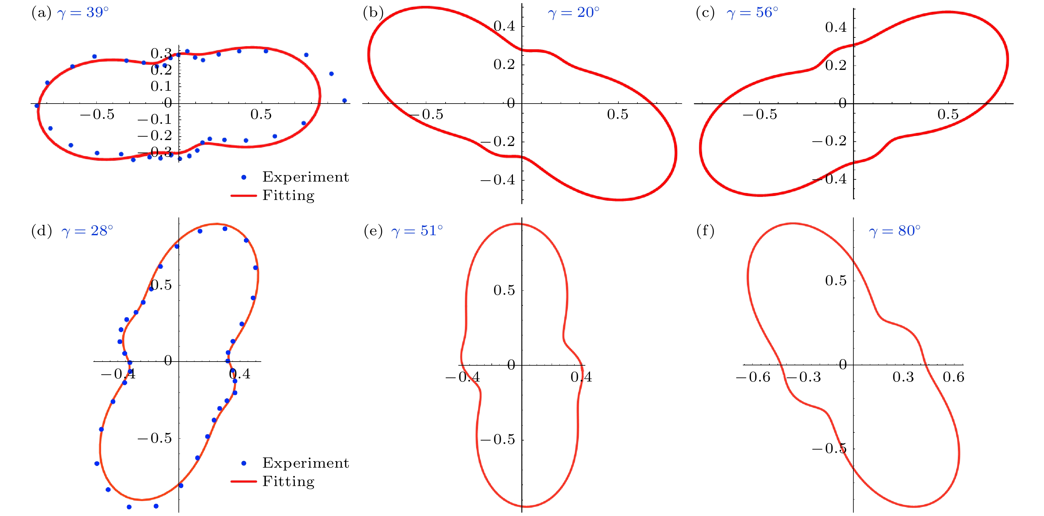
图 2 测得的 SHG 强度与极化角θ的函数关系的极坐标图 (a) CdS纳米线的晶体取向确定为φ = 104°, γ = 39°, ω = 78°, 点代表实验数据, 实线代表理论拟合; (b), (c)相关的理论拟合, 只需改变γ值, 同时保持φ和ω与图(a)相同; (d)取向为φ = 78°, γ = 28°, ω = 85°的另一个CdS纳米线的SHG花型图; (e), (f)理论拟合, 只需改变γ值, 同时保持φ和ω与图(d)相同
Figure 2. Polarization-dependent SHG patterns in different single CdS nanowires: (a) Crystal orientation of CdS nanowires is determined as φ = 104°, γ = 39°, ω = 78°, the points represent experimental data and the solid lines represent theoretical fittings; (b), (c) related theoretical fittings, only changing γ values while keeping φ and ω the same as panel (a); (d) the orientation is φ = 78°, γ = 28°, SHG pattern of another CdS nanowire with ω = 85°; (e), (f) theoretical fittings with different γ values, while φ and ω are remained the same as panel (d).
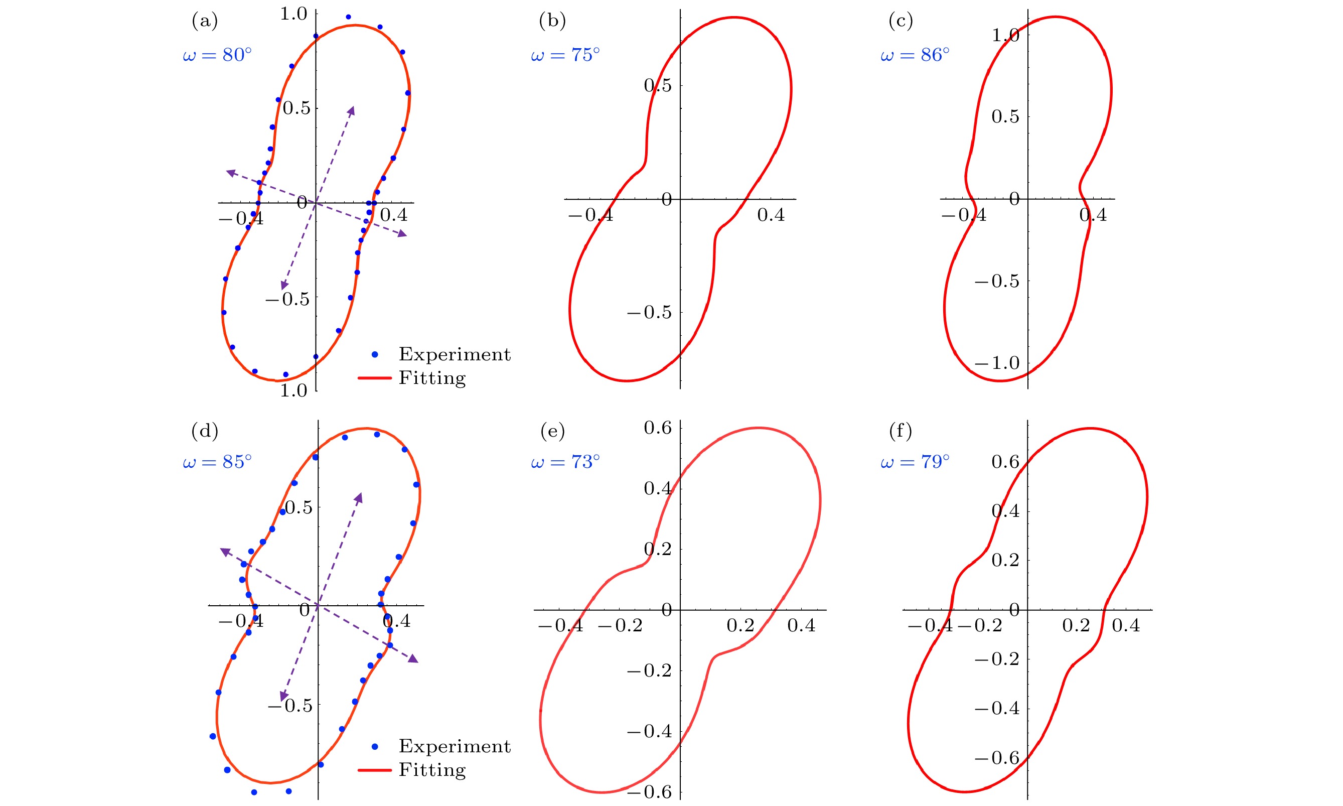
图 3 不同单根CdS纳米线中偏振相关的SHG强度随偏振角θ的变化 (a) CdS纳米线的晶体取向确定为φ = 74°, γ = 39°, ω = 80°, 点代表实验数据, 实线代表理论拟合; (b), (c)相关的理论拟合, 只需改变ω值, 同时保持φ和γ与图(a)相同; (d)取向为φ = 78°, γ = 28°, ω = 85°的另一个CdS纳米线的SHG花型图; (e), (f)理论拟合, 只需改变 ω 值, 同时保持φ和γ与图(d)中相同
Figure 3. Polarization-dependent SHG patterns in different single CdS nanowires: (a) Crystal orientation of CdS nanowires is determined as φ = 74°, γ = 39°, ω = 80°, the points represent experimental data and the solid lines represent theoretical fittings; (b), (c) related theoretical fittings, only changing ω values while keeping φ and γ the same as panel (a); (d) the orientation is φ = 78°, γ = 28°, SHG pattern of another CdS nanowire with ω = 85°; (e), (f) theoretical fittings with different ω values, while φ and γ are remained the same as panel (d).
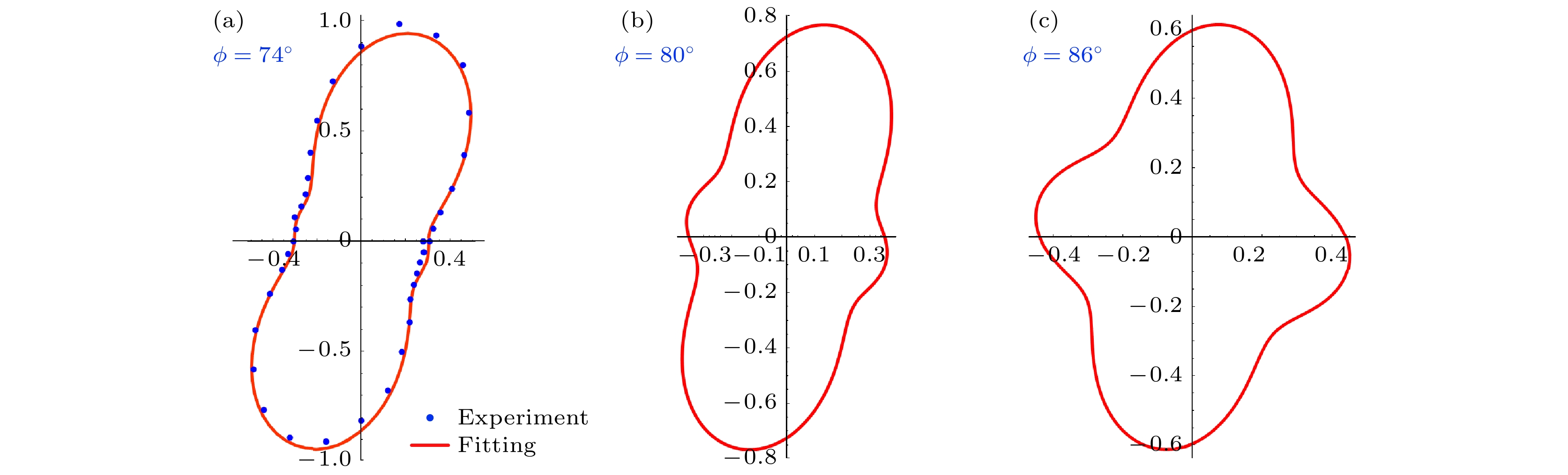
图 4 测量的SHG强度作为偏振角的函数的极坐标图 (a)晶体取向为 φ = 74°, γ = 39°, ω = 80°的单根CdS纳米线的SHG图形, 点代表实验数据, 实线代表理论拟合; (b), (c)相关的理论拟合, 只需改变φ的值, 同时保持γ和ω与图(a)中的相同
Figure 4. Measured SHG strength as a function of the polarization angle θ is shown in polar coordinates: (a) SHG pattern of a single CdS nanowire with the crystal orientation φ = 74°, γ = 39°, ω = 80° is obtained, points represent experimental data, while the solid lines represent theoretical fittings; (b), (c) theoretical fits with different φ values, while γ and ω are remained the same as panel (a).
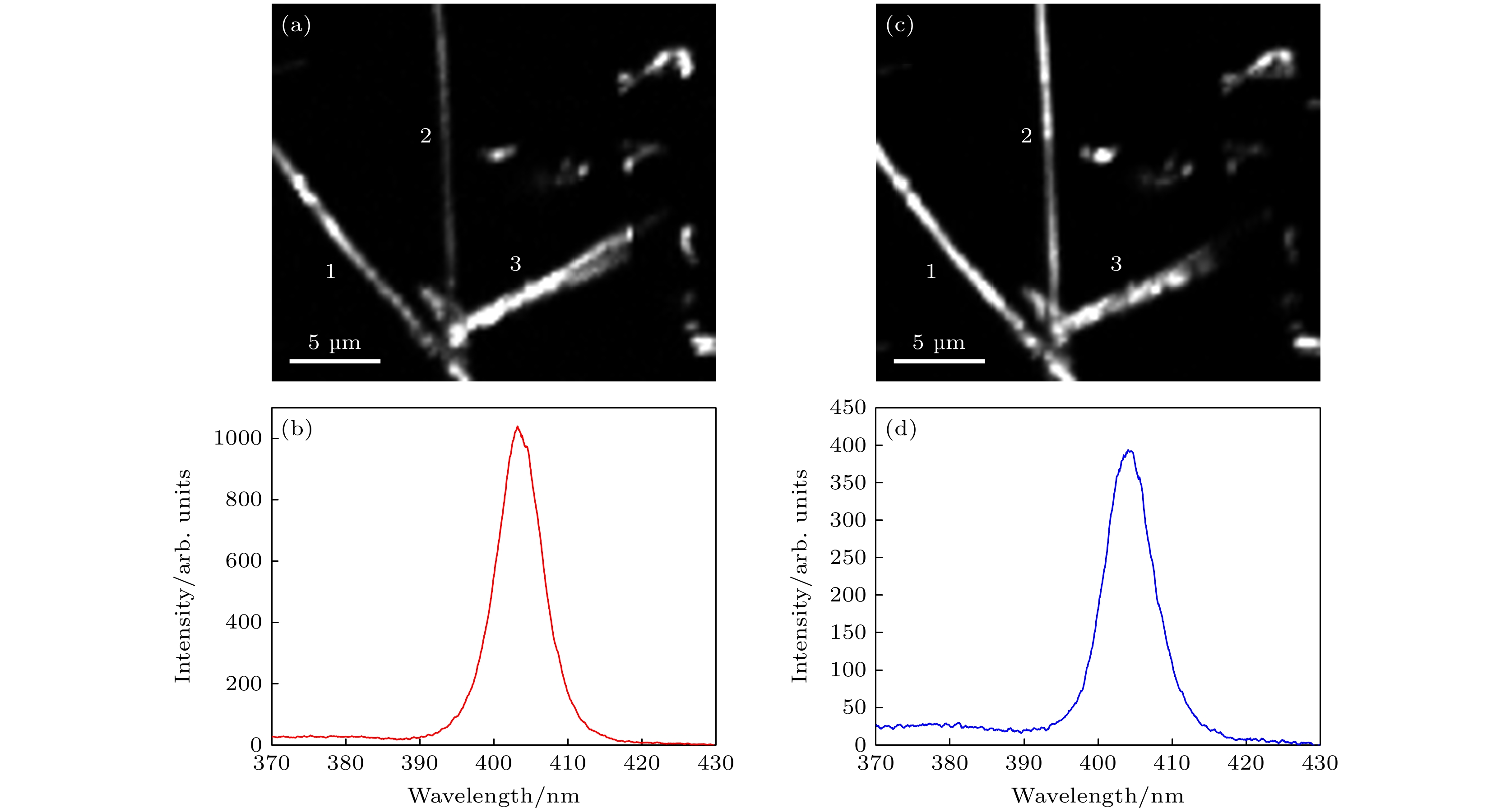
图 5 不同偏振方向下CdS纳米线的SHG显微成像图与相应光谱图 (a)偏振方向角为0°的SHG显微成像图; (b) 偏振方向角为0°的SHG光谱; (c)偏振方向角为45°的SHG显微成像图; (d) 偏振方向角为45°的SHG光谱
Figure 5. SHG microscopic image of CdS nanowire under different polarization angle of input laser: (a) SHG microscopic image of CdS nanowire with polarization angle at 0°; (b) SHG spectrum of CdS nanowire with polarization angle at 0°; (c) SHG microscopic image of CdS nanowire with polarization angle at 45°; (d) SHG spectrum of CdS nanowire with polarization angle at 45°.
-
[1] 白瑞雪, 杨珏晗, 魏大海, 魏钟鸣 2020 物理学报 69 184211
Google Scholar
Bai R X, Yang Y H, Wei D H, Wei Z M 2020 Acta Phys. Sin. 69 184211
Google Scholar
[2] Fan X, Zhang M L, Shafiq I, Zhang W J, Lee C S, Lee S T 2009 Cryst. Growth Des. 9 1375
Google Scholar
[3] Lin Y F, Song J, Ding Y, Lu S Y, Zhang Z L 2008 Adv. Mater. 20 3127
Google Scholar
[4] Zhai T Y, Gu Z J, Zhong H Z, Dong Y, Ma Y, Fu H B, Li Y F, Yao J N 2007 Cryst. Growth Des. 7 488
Google Scholar
[5] Lin Y F, Song J, Ding Y, Lu S Y, Zhang Z L 2008 Appl. Phys. Lett. 92 022105
Google Scholar
[6] Zhai T Y, Fang X S, Li L, Bando Y, Golberg D 2010 Nanoscale 2 168
Google Scholar
[7] Ma R M, Wei X L, Dai L, Dai L, Huo H B, Qin G G 2007 Nanotechnology 18 205605
Google Scholar
[8] Li H Q, Wang X, Xu J Q, Zhang Q, Bando Y, Golberg D 2013 Adv. Mater. 25 3017
Google Scholar
[9] Nakayama Y, Pauzauskie P, Radenovic A, Onorato R M, Saykally R J, Liphardt J, Yang P D 2007 Nature 447 1098
Google Scholar
[10] Prasanth R, van Vugt L K, Vanmaekelbergh D A M, Gerritsen H C 2006 Appl. Phys. Lett. 88 181501
Google Scholar
[11] Tian B Z, Zheng X L, Kempa T J, Fang Y, Yu N F, Yu G H, Huang J L, Lieber C M 2007 Nature 449 885
Google Scholar
[12] Allen J E, Hemesath E R, Perea D E, Lensch-Falk J L, Liz Y, Yin F, Gass M H, Wang P, Bleloch A L, Palmer R E, Lauhon L J 2008 Nat. Nanotechnol. 3 168
Google Scholar
[13] Mu S, Chang J C, Lee S T 2008 Nano Lett. 8 104
Google Scholar
[14] Peng K Q, Wang X, Wu X L, Lee S T 2009 Nano Lett. 9 3704
Google Scholar
[15] Nadia M J, Nada H 2018 International Conference on Materials Engineering and Science Istanbul Turkey, August 8–11, 2018 p012111
[16] Hu H B, Wang K, Long H, Liu W W, Wang B, Lu P X 2015 Nano Lett. 15 3351
Google Scholar
[17] Bautista G, Makitalo J, Chen Ya, Dhaka V, Grasso M, Karvonen L, Jiang H, Huttunen M J, Huhtio T, Lipsanen H, Kauranen M 2015 Nano Lett. 15 1564
Google Scholar
[18] Kim W, Ng J K, Kunitake M E, Conklin B R, Yang P D 2007 J. Am. Chem. Soc. 129 7728
Google Scholar
[19] Jung Y, Tong L, Tanaudommongkon A, Cheng J X, Yang C 2009 Nano Lett. 9 2440
Google Scholar
[20] Xu J Y, Rechav K, Popovitz-Biro R, Nevo I, Feldman Y, Joselevich E 2018 Adv. Mater. 30 1800413
Google Scholar
[21] Wang J J, Zhang X, Deng J B, Hu X, Hu Y, Mao J, Ma M, Gao Y H, Wei Y C, Li F, Wang Z H, Liu X L, Xu J Y, Ren L Q 2021 Molecules 26 5178
Google Scholar
[22] Shoji I, Kondo T, Ito R 2002 Opt. Quant. Electron. 34 797
Google Scholar

 DownLoad:
Catalog
Metrics
- Abstract views: 4672
- PDF Downloads: 232
- Cited By: 0
