


-
基于拓扑绝缘体材料的约瑟夫森结是寻找马约拉纳零能模的候选器件, 因而受到拓扑量子计算研究领域的关注. 这方面实验的关键之一, 是制备具有优质结区的约瑟夫森器件. 本工作在三维拓扑绝缘体Bi2Te3和Bi2(SexTe1–x)3纳米线上制作了约瑟夫森结器件, 研究了其结区的超导邻近效应、多重安德列夫反射和超流-相位关系, 观测到了约瑟夫森结的临界超流随磁场增大而反常地增大、其交流约瑟夫森效应出现半整数的夏皮洛台阶的实验结果. 本文还讨论了这些反常现象的可能来源, 特别是与结区界面处超导电极的Ti缓冲层和拓扑绝缘体纳米线中的Te元素形成TiTe铁磁性合金层的关系.Topological insulator-based Josephson junction, as a candidate device for searching for Majorana zero energy modes, has attracted much attention. One of the key issues along this direction is to fabricate Josephson junctions with high-quality interfaces, hoping to searching for 4π-period current-phase relation in topologically non-trivial Josephson junction. In this work, the Josephson junctions based on three-dimensional topological insulator nanowires Bi2Te3 and Bi2(SexTe1–x)3 are fabricated to study their superconducting proximity effects, multiple Andreev reflections, and current-phase relations. A number of interesting phenomena are observed, including the anomalous enhancement in junctions’ critical supercurrent with magnetic field, and the appearance of half-integer Shapiro steps in the ac Josephson effect. And, we discuss the possible origins of the observed anomalous behaviors in general, and their relation with the ferromagnetic layer of TiTe alloy formed at the interface between the topological insulator nanowires and the Ti buffer layer of the metallic electrodes, in particular. We provide the experimental evidence for the formation of a ferromagnetic TiTe alloy layer at the interface of our device. And, we believe that the formation of such a layer in our Josephson device breaks the time reversal symmetry, leading to the observed anomalous enhancement of the critical supercurrent with magnetic field, as well as the appearance of half-integer Shapiro steps. Our results suggest that to study the topologically non-trivial behaviors such as 4π-period current-phase relation, one still needs to improve the interface quality of the superconductor-normal metal-superconductor type of Josephson junction devices.
-
Keywords:
- topological insulator nanowire /
- anomalous behaviors in critical supercurrent /
- half-integer Shapiro steps
[1] Fu L, Kane C L 2008 Phys. Rev. Lett. 100 096407
 Google Scholar
[2] Zhang H B, Yu H L, Bao D H, Li S W, Wang C X, Yang G W 2012 Phys. Rev. B 86 075102
Google Scholar
[3] Barreto L, Kühnemund L, Edler F, et al. 2014 Nano Lett. 14 3755
Google Scholar
[4] Lu H Z, Shen S Q 2011 Phys. Rev. B 84 125138
Google Scholar
[5] Brahlek M, Kim Y S, Bansal N, Edrey E, Oh S 2011 Appl. Phys. Lett. 99 012109
Google Scholar
[6] Krumrain J, Mussler G, Borisova S, et al. 2011 J. Cryst. Growth 324 115
Google Scholar
[7] Chen X, Ma X C, He K, Jia J F, Xue Q K 2011 Adv. Mater. 23 1162
Google Scholar
[8] Kong D, Randel J C, Peng H, Cha J J, Meister S, Lai K, Chen Y, Shen Z X, Manoharan H C, Cui Y 2010 Nano Lett. 10 329
Google Scholar
[9] Schönherr P, Collins-Mclntyre L J, Zhang S L, Kusch P, Reich S, Giles T, Daisenberger D, Prabhakaran D, Hesjedal T 2014 Nanoscale Res. Lett. 9 127
Google Scholar
[10] Han K B, Chong S K, Oliynyk A O, et al. 2018 Sci. Rep. 8 17290
Google Scholar
[11] Urkude R R, Rawat R, Palikundwar U A 2017 J. Phys. Condens. Matter 29 495602
Google Scholar
[12] Galletti L, Charpentier S, Song Y, Golubev D, Wang S M, Bauch T, Lombardi F 2017 IEEE Trans. Appl. Supercond. 27 1800404
Google Scholar
[13] Kunakova G, Bauch T, Trabaldo E, Andzane J, Erts D, Lombardi F 2019 Appl. Phys. Lett. 115 172601
Google Scholar
[14] Bai M, Wei X K, Feng J, Luysberg M, Bliesener A, Lippertz G, Uday A, Taskin A A, Mayer J, Ando Y 2022 Commun. Mater. 3 20
Google Scholar
[15] Noh H J, Jeong J, Cho E J, Kim K, Min B I, Park B G 2017 Phys. Rev. Lett. 119 016401
Google Scholar
[16] Leng H, Paulsen C, Huang Y K, de Visser A 2017 Phys. Rev. B 96 220506
Google Scholar
[17] Bai M, Yang F, Luysberg M, Feng J, Bliesener A, Lippertz G, Taskin A A, Mayer J, Ando Y 2020 Phys. Rev. Mater. 4 094801
Google Scholar
[18] Niebler G, Cuniberti G, Novotný T 2009 Supercond. Sci. Technol. 22 085016
Google Scholar
[19] Xuan X, Zhang Z, Chen C, Guo W 2022 Nano Lett. 22 5379
Google Scholar
[20] English C D, Hamilton D R, Chialvo C, Moraru I C, Mason N, Harlingen D J V 2016 Phys. Rev. B 94 115435
Google Scholar
[21] Spanton E M, Deng M, Vaitiekėnas S, Krogstrup P, Nygård J, Marcus C M, Moler K A 2017 Nat. Phys. 13 1177
Google Scholar
[22] Chen A Q, Park M J, Gill S T, et al. 2018 Nat. Commun. 9 3478
Google Scholar
[23] Hart S, Ren H, Kosowsky M, et al. 2017 Nat. Phys. 13 87
Google Scholar
[24] Trimble C J, Wei M T, Yuan N F Q, et al. 2021 NPJ Quantum Mater. 6 61
Google Scholar
[25] Yao Y, Cai R, Yang S H, Xing W, Ma Y, Mori M, Ji Y, Maekawa S, Xie X C, Han W 2021 Phys. Rev. B 104 104414
Google Scholar
-

图 1 (a), (b)分别为基于Bi2(SexTe1–x)3纳米线和Bi2Te3纳米线约瑟夫森结器件的SEM图, 以及各自对应的微分电阻随偏置电流和磁场而变化的实验数据, 其中Ib为直流偏置电流, iac为低频交流电流, V为结区电压, B为施加的磁场
Fig. 1. (a) and (b) Scanning electron microscope images of two Josephson junction devices based on Bi2(SexTe1–x)3 nanowire and Bi2Te3 nanowire, respectively, together with their differential resistance as a function of bias current and magnetic field. Ib, iac, V and B represent dc bias current, low-frequency ac current, voltage drop across the junction, and applied magnetic field, respectively.
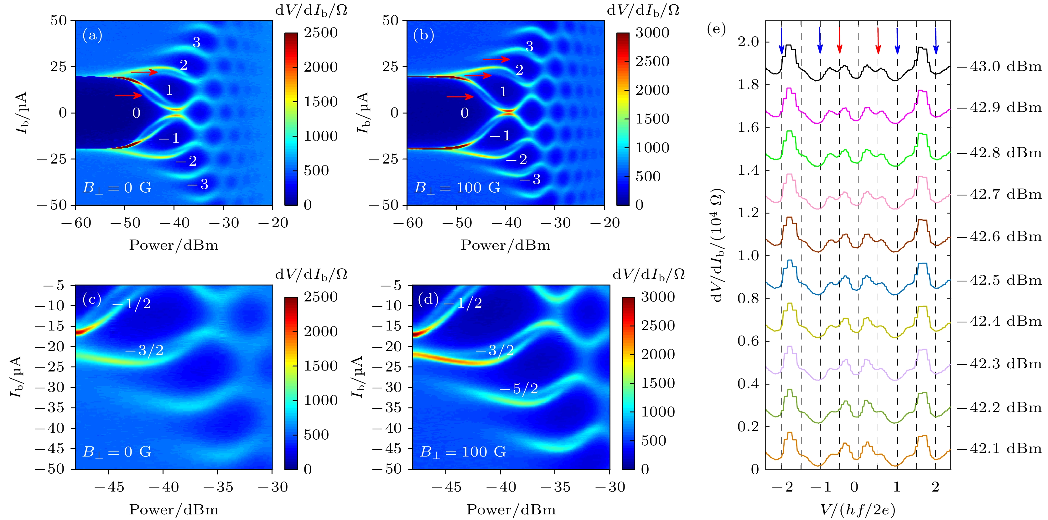
图 2 图1(b)中的器件在微波辐射下出现整数和半整数的夏皮洛台阶 (a), (b)分别为0 G和100 G垂直磁场下的微分电阻随微波功率和偏置电流而变化的实验数据, 白色数字标示的深蓝色区是对应序号的整数台阶出现的区域, 红色箭头标示的是半整数台阶出现的位置; (c), (d)是(a), (b)局部的放大图, 展示在100 G的垂直磁场下, 半整数台阶比零磁场下更为清晰; (e) 图(a)中几个不同微波功率处的微分电阻随偏置电压的变化关系曲线, 红色箭头标记的是半整数台阶出现的位置, 蓝色箭头标记的是整数台阶出现的位置
Fig. 2. Integer and half-integer Shapiro steps under microwave irradiation for the device shown in Fig. 1(b): (a), (b) The differential resistance as a function of microwave power and bias current under the perpendicular magnetic field of 0 G and 100 G, respectively, showing Shapiro steps. Integer steps appear in the dark blue regions indicated by the white numbers. And, half-integer steps appear in the positions indicated by the red arrows. (c), (d) Details of (a) and (b), showing that the half-integer steps can be more clearly seen in a perpendicular magnetic field of 100 G than in zero field. (e) Line-cuts in panel (a) at several different microwave powers and converted to bias voltage. Integer and half-integer Shapiro steps are marked with blue and red arrows, respectively.
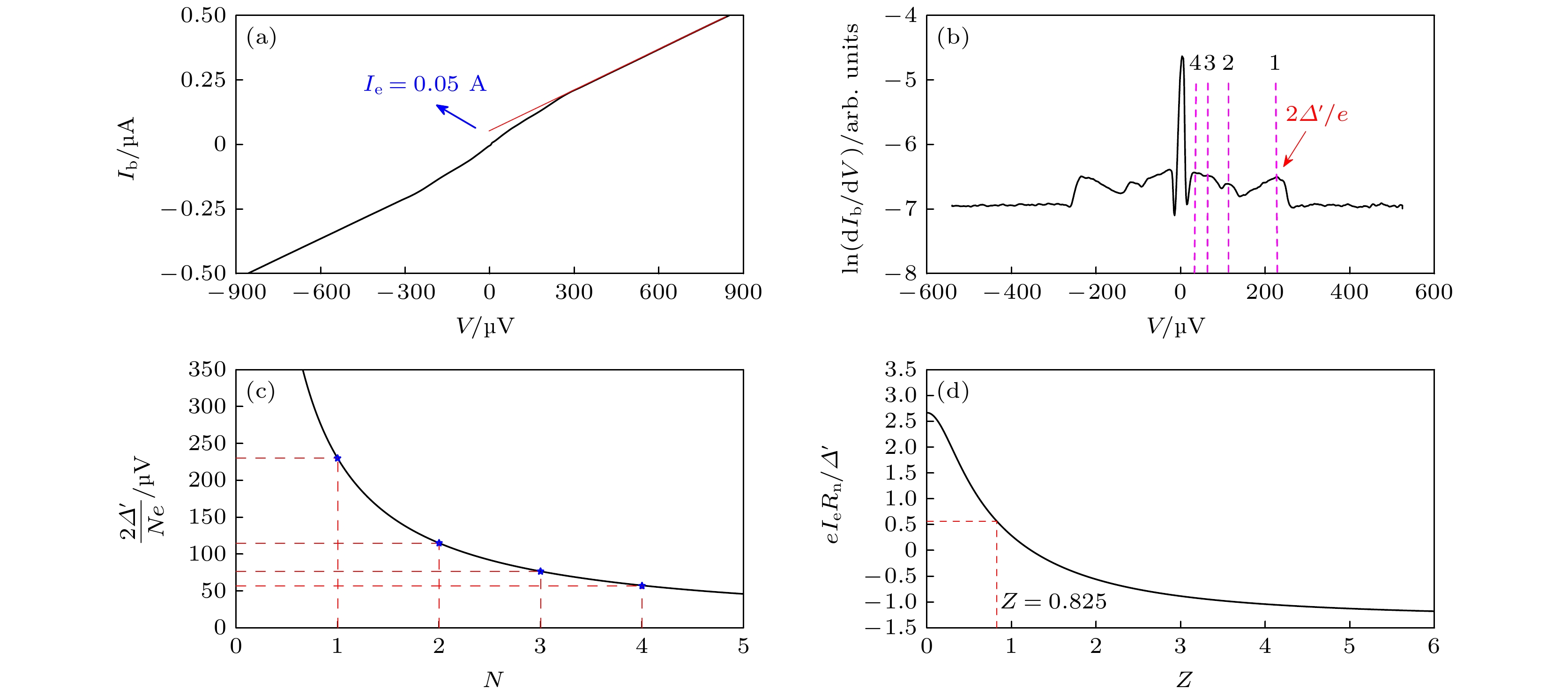
图 3 多重安德列夫反射 (a)基于图1(b)约瑟夫森结器件的Ib-V曲线, 过量电流为50 nA; (b)多重安德列夫反射导致的电导峰; (c)电压峰的电压位置与电导峰的序号符合理论预计; (d)根据OTBK理论得出的
$ e{I_{\text{e}}}{R_{\text{n}}}/\varDelta ' $ -Z的曲线[18]Fig. 3. Multiple Andreev reflection: (a) The Ib-V curve of the Josephson junction device shown in Fig. 1(b), the excess current Ie is 50 nA; (b) the conductance peaks caused by multiple Andreev reflections; (c) the peak positions follow the expectation of the theory; (d) the
$ e{I_{\text{e}}}{R_{\text{n}}}/\varDelta ' $ -Z curve derived from OTBK theory[18].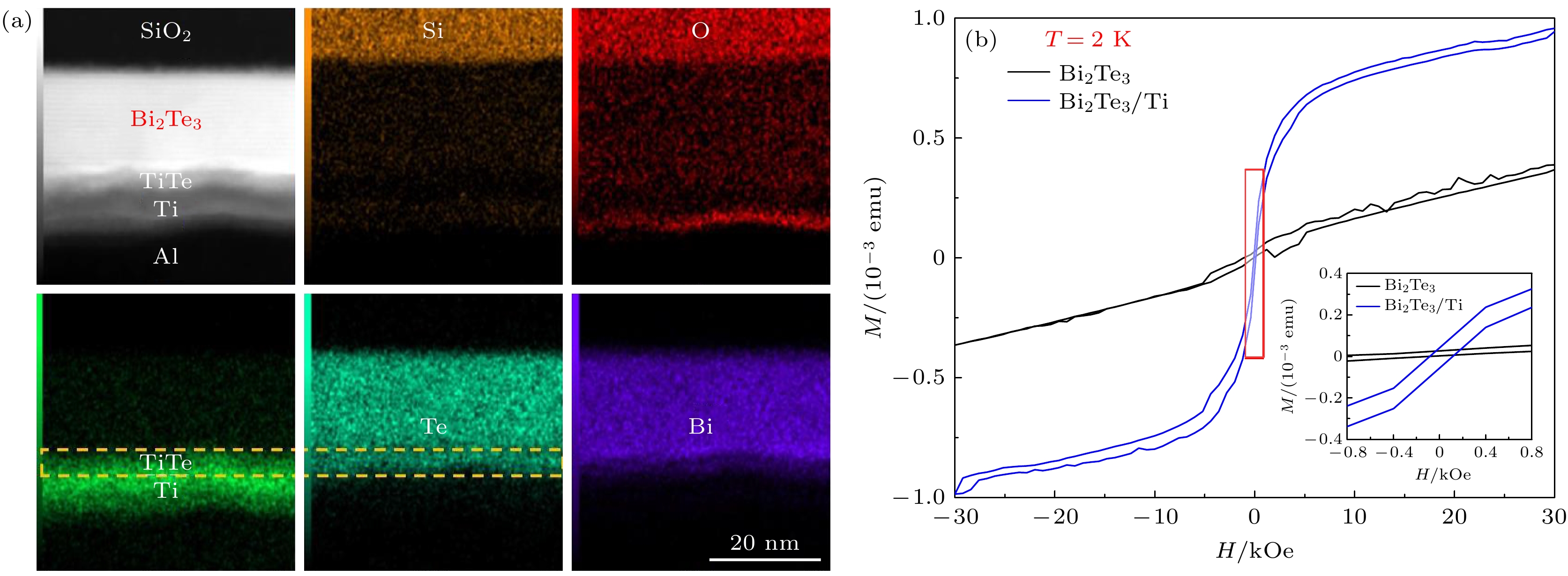
图 4 (a)基于三维Bi2Te3纳米线约瑟夫森器件截面的TEM图以及能谱分析的元素成分面扫描图, Bi2Te3与电极缓冲层Ti的界面处产生了TiTe合金层, 位置如图中黄色虚线框所示; (b) Bi2Te3薄片样品和蒸镀Ti后的Bi2Te3/Ti异质结样品在2 K温度下的M-H曲线数据图(1 emu = 10–3 A·m2), 插图为红色方框区域实验数据放大图
Fig. 4. (a) Transmission electron microscope image on the cross-section of the Josephson junction device composed of a three-dimensional topological insulator nanowire Bi2Te3 and superconducting electrodes with buffer layer Ti at the interface. Also shown are the elemental mappings at the interface by energy dispersive spectroscopy. The two dashed yellow lines indicate where TiTe alloy is formed at the interface; (b) the M-H curves measured at the temperature of 2 K on a Bi2Te3 flake before and after Ti film deposition, the inset shows the enlarged details in the red box.
-
[1] Fu L, Kane C L 2008 Phys. Rev. Lett. 100 096407
Google Scholar
[2] Zhang H B, Yu H L, Bao D H, Li S W, Wang C X, Yang G W 2012 Phys. Rev. B 86 075102
Google Scholar
[3] Barreto L, Kühnemund L, Edler F, et al. 2014 Nano Lett. 14 3755
Google Scholar
[4] Lu H Z, Shen S Q 2011 Phys. Rev. B 84 125138
Google Scholar
[5] Brahlek M, Kim Y S, Bansal N, Edrey E, Oh S 2011 Appl. Phys. Lett. 99 012109
Google Scholar
[6] Krumrain J, Mussler G, Borisova S, et al. 2011 J. Cryst. Growth 324 115
Google Scholar
[7] Chen X, Ma X C, He K, Jia J F, Xue Q K 2011 Adv. Mater. 23 1162
Google Scholar
[8] Kong D, Randel J C, Peng H, Cha J J, Meister S, Lai K, Chen Y, Shen Z X, Manoharan H C, Cui Y 2010 Nano Lett. 10 329
Google Scholar
[9] Schönherr P, Collins-Mclntyre L J, Zhang S L, Kusch P, Reich S, Giles T, Daisenberger D, Prabhakaran D, Hesjedal T 2014 Nanoscale Res. Lett. 9 127
Google Scholar
[10] Han K B, Chong S K, Oliynyk A O, et al. 2018 Sci. Rep. 8 17290
Google Scholar
[11] Urkude R R, Rawat R, Palikundwar U A 2017 J. Phys. Condens. Matter 29 495602
Google Scholar
[12] Galletti L, Charpentier S, Song Y, Golubev D, Wang S M, Bauch T, Lombardi F 2017 IEEE Trans. Appl. Supercond. 27 1800404
Google Scholar
[13] Kunakova G, Bauch T, Trabaldo E, Andzane J, Erts D, Lombardi F 2019 Appl. Phys. Lett. 115 172601
Google Scholar
[14] Bai M, Wei X K, Feng J, Luysberg M, Bliesener A, Lippertz G, Uday A, Taskin A A, Mayer J, Ando Y 2022 Commun. Mater. 3 20
Google Scholar
[15] Noh H J, Jeong J, Cho E J, Kim K, Min B I, Park B G 2017 Phys. Rev. Lett. 119 016401
Google Scholar
[16] Leng H, Paulsen C, Huang Y K, de Visser A 2017 Phys. Rev. B 96 220506
Google Scholar
[17] Bai M, Yang F, Luysberg M, Feng J, Bliesener A, Lippertz G, Taskin A A, Mayer J, Ando Y 2020 Phys. Rev. Mater. 4 094801
Google Scholar
[18] Niebler G, Cuniberti G, Novotný T 2009 Supercond. Sci. Technol. 22 085016
Google Scholar
[19] Xuan X, Zhang Z, Chen C, Guo W 2022 Nano Lett. 22 5379
Google Scholar
[20] English C D, Hamilton D R, Chialvo C, Moraru I C, Mason N, Harlingen D J V 2016 Phys. Rev. B 94 115435
Google Scholar
[21] Spanton E M, Deng M, Vaitiekėnas S, Krogstrup P, Nygård J, Marcus C M, Moler K A 2017 Nat. Phys. 13 1177
Google Scholar
[22] Chen A Q, Park M J, Gill S T, et al. 2018 Nat. Commun. 9 3478
Google Scholar
[23] Hart S, Ren H, Kosowsky M, et al. 2017 Nat. Phys. 13 87
Google Scholar
[24] Trimble C J, Wei M T, Yuan N F Q, et al. 2021 NPJ Quantum Mater. 6 61
Google Scholar
[25] Yao Y, Cai R, Yang S H, Xing W, Ma Y, Mori M, Ji Y, Maekawa S, Xie X C, Han W 2021 Phys. Rev. B 104 104414
Google Scholar

 下载:
下载:


计量
- 文章访问数: 2923
- PDF下载量: 88
- 被引次数: 0
