


-
在大气压介质阻挡放电的实际应用中, 等离子体通常作用于非平滑表面. 其表面形貌导致的电场畸变和表面电荷分布不均匀, 会对放电的均匀稳定产生不利影响. 建立了下介质板为波浪状的大气压氦气介质阻挡放电仿真模型, 并采用正弦削波电压对放电均匀性进行调控. 结果表明: 相比于未削波情况下, 放电均匀性提高, 介质阻挡放电从柱状放电模式转换为准均匀放电模式. 这可以归因于气隙电压降低而产生的不完全放电消散; 随后的电子回流过程使残余空间电子与表面电荷中和, 限制了表面电荷积累. 随着削波比例增加, 表面电荷分布更为均匀, 进而导致电场分布在径向上波动减弱. 此外, 在一定削波范围内放电效率也有所提高. 本研究揭示了削波电压对非平滑表面介质阻挡放电的影响机理, 为介质阻挡放电均匀性调控提供了新的思路.In practical applications of dielectric barrier discharges under atmospheric pressure, plasma usually acts on non-smooth surfaces. The electric field distortion and uneven surface charge distribution caused by its surface morphology will create an adverse effect on the uniformity and stability of the discharge. In this paper, we establish a simulation model of atmospheric pressure helium dielectric barrier discharge on a wavy lower dielectric plate, and use a sinusoidal clipping voltage to regulate the discharge uniformity. The results show that the discharge uniformity is improved compared with the unclipped case, and the discharge mode is changed from columnar mode to quasi-uniform mode. This can be attributed to the incomplete discharge dissipation caused by the reduction of air gap voltage; the subsequent electron backflow process neutralizes the the residual space electrons with the surface charge, which limits the accumulation of surface charges. With the increase of clipping ratio, the surface charge distribution becomes more uniform, and the radial fluctuation of electric field distribution weakens. In addition, the discharge efficiency is improved in a certain clipping range. This study reveals the mechanism of clipping voltage influence on non-smooth surface discharge, and provides a new idea for regulating the uniformity of dielectric barrier discharge.
-
Keywords:
- dielectric barrier discharge /
- non-smooth surface /
- clipping voltage /
- uniformity of discharge
[1] 梅丹华, 方志, 邵涛 2020 中国电机工程学报 40 1339
 Google Scholar
Mei D H, Fang Z, Shao T 2020 Chin. Soc. Elec. Eng. 40 1339
Google Scholar
[2] 戴栋, 宁文军, 邵涛 2017 电工技术学报 32 1
Google Scholar
Dai D, Ning W J, Shao T 2017 Trans. Chin. Elc. Soc. 32 1
Google Scholar
[3] 李和平, 于达仁, 孙文廷, 刘定新, 李杰, 韩先伟, 李增耀, 孙冰, 吴云 2017 高电压技术 42 3697
Google Scholar
Li H P, Yu D L, Sun W T, Liu D X, Li J, Han X W, Li Z Y, Sun B, Wu Y 2017 High Voltage Eng. 42 3697
Google Scholar
[4] Adamovich I, Agarwal S, Ahedo E, et al. 2022 J. Phys. D: Appl. Phys. 55 373001
Google Scholar
[5] Larouss M, Bekeschus S, Bogaerts A, Keidar M, Bogaerts A, Fridman A, Lu B X 2022 IEEE Trans. Radiat. Plasma Med. Sci. 6 127
Google Scholar
[6] Sanito R C, You S J, Wang Y F 2021 J. Environ. Manage. 288 112380
Google Scholar
[7] Laroussi M, Lu X, Keidar M 2017 J. Appl. Phys. 122 020901
Google Scholar
[8] Gaunt L F, Beggs C B, Georghiou G E 2006 IEEE Trans. Plasma Sci. 34 1257
Google Scholar
[9] Ouyang J T, Li B, He F, Dai D 2018 Plasma Sci. Technol. 20 103002
Google Scholar
[10] Fang Z, Qiu Y, Zhang C, Kuffel E 2007 J. Phys. D:Appl. Phys. 40 1401
Google Scholar
[11] Wang Q, Ning W J, Dai D, Zhang Y H, Ouyang J T 2019 J. Phys. D: Appl. Phys. 52 205201
Google Scholar
[12] Zhang Y H, Ning W J, Dai D, Wang Q 2019 Plasma Sources Sci. Technol. 28 075003
Google Scholar
[13] Zhang Y H, Neyts E C, Bogaerts A 2016 J. Phys. Chem. C 120 25923
Google Scholar
[14] Hao Y P, Zheng B, Liu Y G 2014 Phys. Plasmas 21 013503
Google Scholar
[15] Zhang P, Kortshagen U 2006 J. Phys. D: Appl. Phys. 39 153
Google Scholar
[16] Zhang J, Wang Y H, Wang D Z 2015 Phys. Plasmas 22 043517
Google Scholar
[17] Brauer I, Punset C, Purwins H G, Boeuf J P 1999 J. Appl. Phys. 85 7569
Google Scholar
[18] Boeuf J P, Bernecker B, Callegari T, Blanco S, Fournier R 2012 Appl. Phys. Lett. 100 244108
Google Scholar
[19] Zhang Y H, Ning W J, Dai D, Wang Q 2019 Plasma Sci. Technol. 21 074003
Google Scholar
[20] Huang Z M, Hao Y P, Han Y Y, Yang L, Tang L, Liao Y F, Li L C 2017 Phys. Plasmas 24 113506
Google Scholar
[21] Ye Q Z, Wu Y F, Li X W, Chen T, Shao G W 2012 Plasma Sources Sci. Technol. 21 065008
Google Scholar
[22] Motrescu I, Ciolan M A, Sugiyama K, Kawamura N, Nagatsu M 2018 Plasma Sources Sci. Technol. 27 115005
Google Scholar
[23] Wang X X, Luo H Y, Liang Z, Mao T, Ma R L 2006 Plasma Sources Sci. Technol. 15 845
Google Scholar
[24] Brandenburg R 2017 Plasma Sources Sci. Technol. 26 053001
Google Scholar
[25] Heinlin J, Morfill G, Landthaler M, Stolz W, Isbary G, Zimmermann J L, Shimizu T, Karrer S 2010 J. Dtsch. Dermatol. Ges. 8 968
Google Scholar
[26] Buendia J A, Venkattraman A 2015 Europhys. Lett. 112 55002
Google Scholar
[27] Fu Y Y, Zhang P, Verboncoeur J P, Christlieb A J, Wang X X 2018 Phys. Plasmas 25 013530
Google Scholar
[28] Fu Y Y, Zhang P, Verboncoeur J P 2018 Appl. Phys. Lett. 113 054102
Google Scholar
[29] Levko D, Raja L L 2015 J. Appl. Phys. 117 173303
Google Scholar
[30] Go D B, Venkattraman A 2014 J. Phys. D: Appl. Phys. 47 503001
Google Scholar
[31] Venkattraman A, Garg A, Peroulis D, Alexeenko A A 2012 Appl. Phys. Lett. 100 083503
Google Scholar
[32] Cheng H, Liu X, Lu X P, Liu D W 2016 Phys. Plasmas 23 073517
Google Scholar
[33] Cheng H, Xu M Y, Pan S H, Lu X P, Liu D W 2018 Plasma Sci. Technol. 20 044006
Google Scholar
[34] Wang Q, Ning W J, Dai D, Zhang Y H 2019 Plasma Process. Polym. 17 1900182
Google Scholar
[35] Mujahid Z, Korolov I, Liu Y, Mussenbrock T, Schulze J 2022 J. Phys. D: Appl. Phys. 55 495201
Google Scholar
[36] Babaeva N Y, Tian W, Kushner M J 2014 J. Phys. D: Appl. Phys. 47 235201
Google Scholar
[37] Babaeva N Y, Kushner M J 2013 J. Phys. D:Appl. Phys. 46 025401
Google Scholar
[38] Lin A, Biscop E, Gorbanev Y, Smits E, Bogaerts A 2021 Plasma Process. Polym. 19 e2100151
Google Scholar
[39] Zhang Y H, Ning W J, Dai D, Wang Q 2019 Plasma Sources Sci. Technol. 28 104001
Google Scholar
[40] Kong M G, Deng X T 2003 IEEE Trans. Plasma Sci. 31 7
Google Scholar
[41] Fridman G, Friedman G, Gutsol A, Shekhter A B, Vasilets V N, Fridman A 2008 Plasma Process. Polym. 5 503
Google Scholar
[42] Ning W J, Dai D, Li L C 2018 Plasma Sources Sci. Technol. 27 08LT01
Google Scholar
[43] Cheng H, Liu X, Liu D W, Lu X P 2016 High Volt. 1 62
Google Scholar
[44] Lazarou C, Belmonte T, Chiper A S, Georghiou G E 2016 Plasma Sources Sci. Technol. 25 055023
Google Scholar
[45] 力伯曼, 里登伯格 著 (蒲以康等 译) 2018 等离子体放电与材料工艺原理: 第2版 (北京: 电子工业出版社) 第6—7页
Lieberman M A, Lichtenberg A J (translated by Pu Y K, et al.) 2018 Principles of Plasma Discharges and Materials Processing (2nd Ed.) (Beijing: Publishing House of Electronics Industry) pp6–7 (in Chinese)
[46] Lazarou C, Koukounis D, Chiper A S, Costin C, Topala I, Georghiou G E 2015 Plasma Sources Sci. Technol. 24 035012
Google Scholar
[47] Hagelaar G J M, Pitchford L C 2005 Plasma Sources Sci. Technol. 14 722
Google Scholar
[48] Purwins H G, Stollenwerk L 2014 Plasma Phys. Control. Fusion 56 123001
Google Scholar
[49] Ellis H W, Pai R Y, McDaniel E W, Mason E A, Viehland L A 1976 At. Data Nucl. Data Tables. 17 177
Google Scholar
[50] Yan W, Xia Y, Bi Z H, Song Y, Wang D Z, Sosnin E A, Skakun V S, Liu D P 2017 J. Phys. D: Appl. Phys. 50 345201
Google Scholar
[51] Hagelaar G J M 2000 Phys. Rev. E 62 1452
Google Scholar
[52] Motz H, Wise H 1960 J. Chem. Phys. 32 1893
Google Scholar
[53] Bilici M A, Haase J R, Boyle C R, Go D B, Sankaran R M 2016 J. Appl. Phys. 119 223301
Google Scholar
[54] Boeuf J P, Yang L L, Pitchford L C 2013 J. Phys. D:Appl. Phys. 46 015201
Google Scholar
[55] Petra C G, Schenk O, Anitescu M 2014 Comput. Sci. Eng. 16 32
Google Scholar
[56] Li B, Dong L F, Zhang C, Shen Z K, Zhang X P 2014 J. Phys. D: Appl. Phys. 47 055205
Google Scholar
[57] Huang Z M, Hao Y P, Yang L, Han Y X, Li L C 2015 Phys. Plasmas 22 123519
Google Scholar
[58] Ning W J, Dai D, Zhang Y H, Hao Y P, Li L C 2017 Phys. Plasmas 24 073509
Google Scholar
[59] Golubovskii Y B, Maiorov V A, Behnke J, Behnke J F 2003 J. Phys. D: Appl. Phys. 36 39
Google Scholar
[60] Lee D, Park J M, Hong S H, Kim Y 2005 IEEE Trans. Plasma Sci. 33 949
Google Scholar
[61] Jiang W M, Tang J, Wang Y S, Zhao W, Duan Y X 2013 Phys. Plasmas 20 073509
Google Scholar
[62] Wang Q, Zhou X Y, Dai D, Huang Z, Zhang D M 2021 Plasma Sources Sci. Technol. 30 05LT01
Google Scholar
-

图 3 稳态下DBD在外施电压周期内其平均电子密度的空间分布 (施加10 kHz, 1.5 kV正弦电压) (a)平滑表面DBD; (b) w-DBD
Fig. 3. Spatial distribution of average electron density on DBD over one period of applied voltage at steady state (The voltage source is 10 kHz, 1.5 kV sinusoidal voltage): (a) Smooth surface DBD; (b) w-DBD.
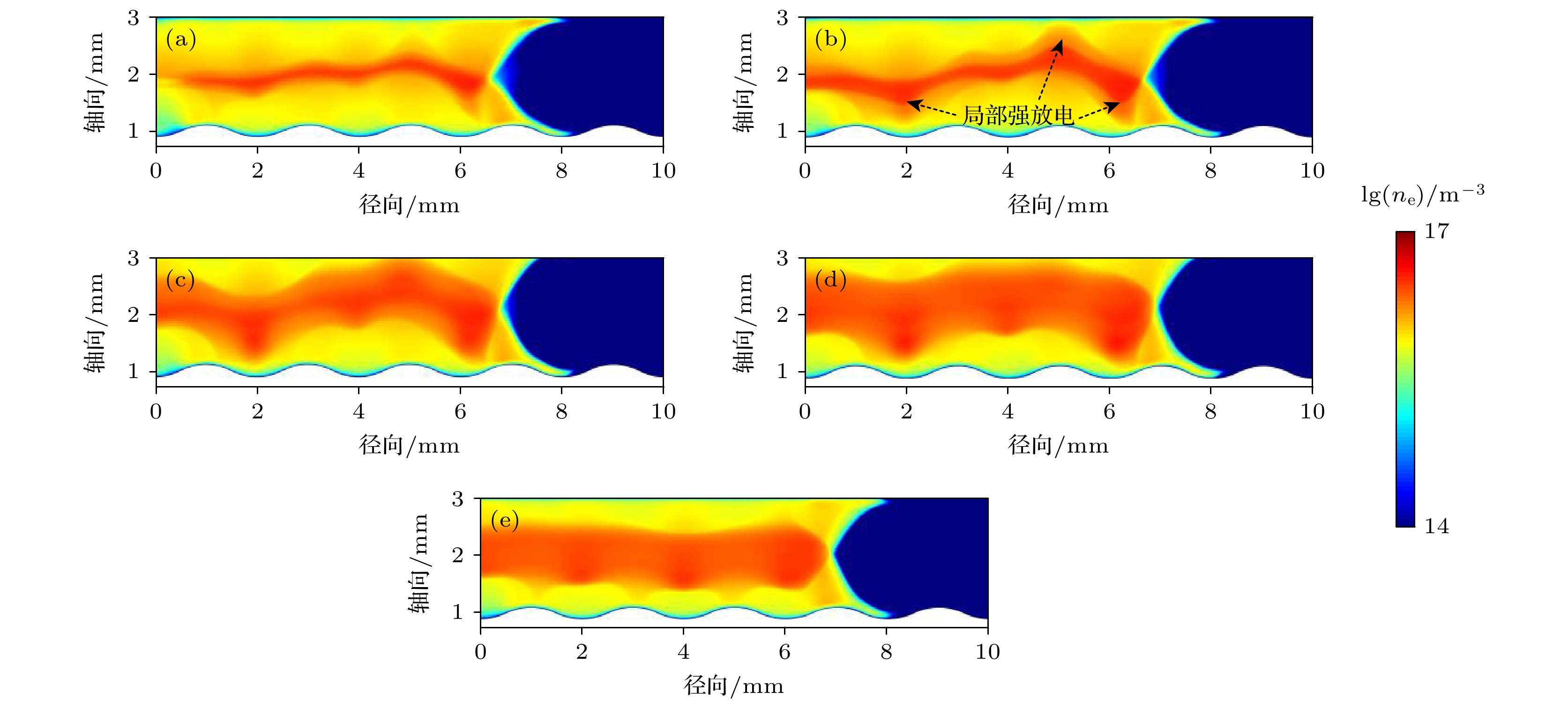
图 4 不同pc下, 放电达到稳态后一个外施电压周期内的平均电子密度的空间分布 (a) pc = 50%; (b) pc = 55%; (c) pc = 60%; (d) pc = 65%; (e) pc = 70%
Fig. 4. Spatial distribution of average electron density over one period of applied voltage at steady state under different pc: (a) pc = 50%; (b) pc=55%; (c) pc = 60%; (d) pc = 65%; (e) pc = 70%.
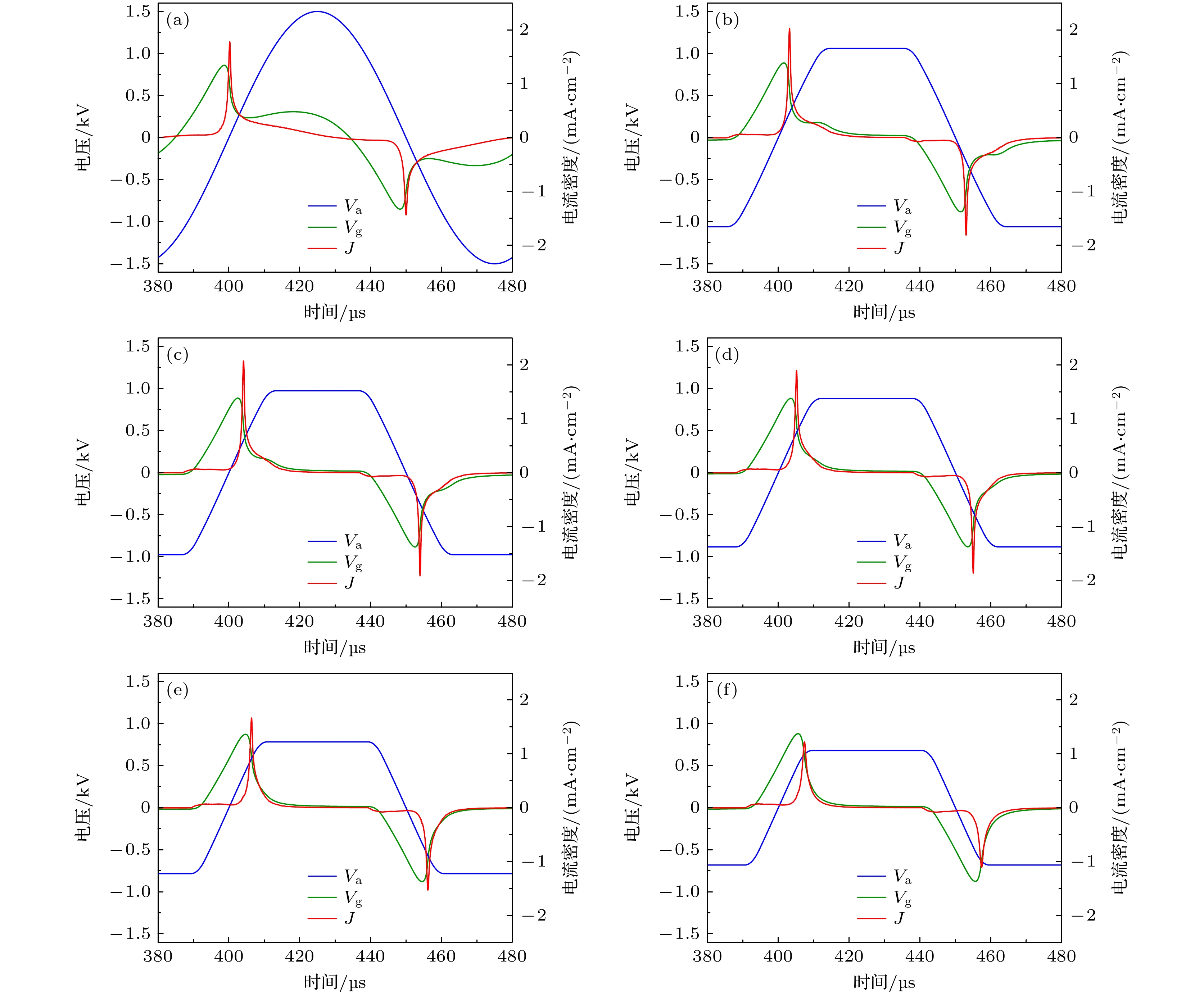
图 5 不同pc下, 放电达到稳态后一个外施电压周期内的外施电压Va, 气隙电压Vg和电流密度J (a) pc = 0; (b) pc = 50%; (c) pc = 55%; (d) pc = 60%; (e) pc = 65%; (f) pc = 70%
Fig. 5. Temporal profiles of applied voltage Va, gap voltage Vg and current density J over one period of applied voltage at steady state under different pc: (a) pc = 0; (b) pc = 50%; (c) pc = 55%; (d) pc = 60%; (e) pc = 65%; (f) pc = 70%.

图 6 pc不同时, 放电达到稳态后一个外施电压周期内的电压电流波形(a), (c), (e)和t1—t5时刻对应的电子密度空间分布(b), (d), (f). 正负号表示该时刻的气隙电压极性 (a), (b) pc = 0; (c), (d) pc = 55%; (e), (f) pc = 70%
Fig. 6. Voltage and current waveform (a), (c), (e) and spatial distribution (b), (d), (f) of electron density corresponding to t1 to t5 over one period of applied voltage at steady state under different pc. Plus and minus signs indicate air gap voltage polarity at this time: (a), (b) pc = 0; (c), (d) pc = 55%; (e), (f) pc = 70%.

图 7 pc分别为0, 55%, 70%时, t1 (a)和t4 (b)时刻对应的净表面电荷密度ρs
Fig. 7. Net surface charge density ρs at t1 (a) and t4 (b) under pc of 0, 55% and 70% respectively.

图 8 pc分别为0, 55%, 70%时 (a1), (b1) t1和t4时刻对应的轴向平均电场强度|Ez|; (a2) t1时刻距上介质板表面0.05 mm附近的径向电场强度Er; (b2) t4时刻距下介质板表面0.05 mm附近的径向电场强度Er
Fig. 8. Under pc of 0, 55% and 70%: (a1), (b1) Axial average electric field |Ez| at t1 and t4 respectively; (a2) radial electric field Er near surface of 0.05 mm upper dielectric plate at t1; (b2) radial electric field Er near surface of 0.05 mm lower dielectric plate at t4.

图 9 pc分别为0, 55%, 70%时, 介质板表面附近的电子通量Γe (a) t1时刻上介质板表面附近(r = 0—8 mm, z = 2—3 mm区域); (b) t4时刻下介质板表面附近(r = 0—8 mm, z = 0.9—2.0 mm区域)
Fig. 9. Electron flux Γe near dielectric plate at pc of 0, 55% and 70%: (a) Near upper dielectric plate (r = 0–8 mm, z = 2–3 mm) at t1; (b) near lower dielectric plate (r = 0–8 mm, z = 0.9–2.0 mm) at t4.

图 10 pc分别为0, 55%, 70%时, t1 (a)和t4 (b)时刻对应的轴向平均种子电子密度ne
Fig. 10. Axial average seed electron density ne at t1 (a) and t4 (b) under pc of 0, 55% and 70% respectively.

图 11 pc分别为0, 55%, 70%时, 正击穿过程中(从预电离阶段开始的半个外施电压周期)局部强放电处的轴向切线的电子密度时空分布, 以及气隙电压极性反转时刻的电子密度ne, 离子密度ni和轴向电场|Ez|的轴向分布 (a) pc = 0; (b) pc = 55%; (c) pc = 70%
Fig. 11. Spatial-temporal distribution of electron density at axial tangent of the partial strong discharge during positive breakdown (half of applied voltage period starting from pre-ionization stage), and axial distribution of electron density ne, ion density ni and axial electric field |Ez| at the time of polarity reversal of the air gap voltage under different pc: (a) pc = 0; (b) pc = 55%; (c) pc = 70%.

图 12 电子回流开始和结束时刻下表面电荷密度分布 (a) pc = 55%; (b) pc = 70%
Fig. 12. Lower surface’s charge density distribution at beginning and the end of electron backflow: (a) pc = 55%; (b) pc = 70%.
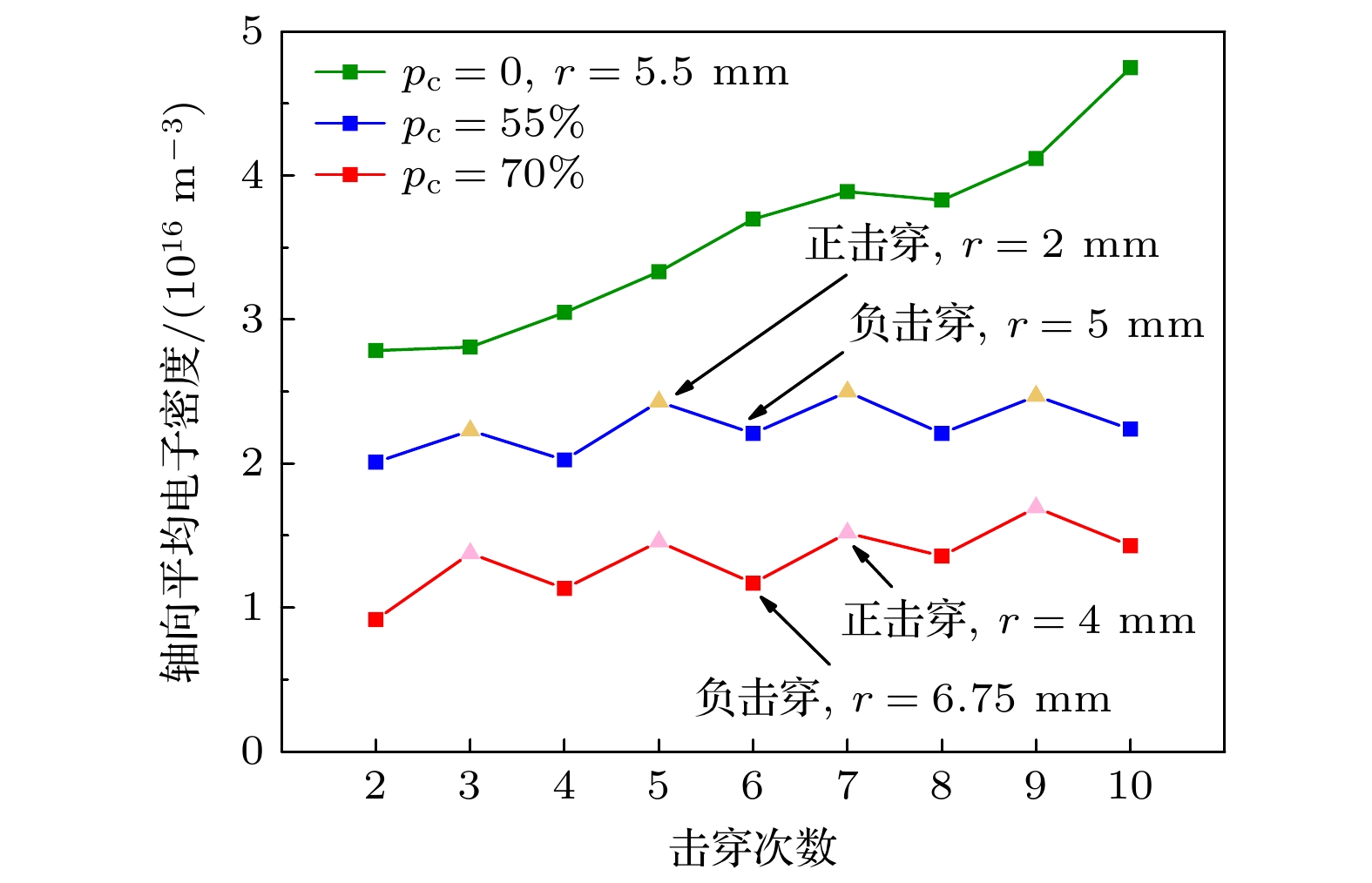
图 13 pc分别为0, 55%, 70%时, 5个周期内局部强放电的击穿强度(以轴向平均电子密度表示, 其中削波电压下选取的正负击穿位置不同)
Fig. 13. Strength of local intense discharge or discharge column within five periods under pc of 0, 55% and 70% respectively (Which is expressed as axial average electron density, and selected positions of positive and negative breakdown under the clipping voltage are different).

图 14 pc分别为0, 55%, 70%时, 放电达到稳态后一个外施电压周期内的彭宁电离速率
Fig. 14. Penning ionization rates over one period of applied voltage at steady state under pc of 0, 55% and 70% respectively.
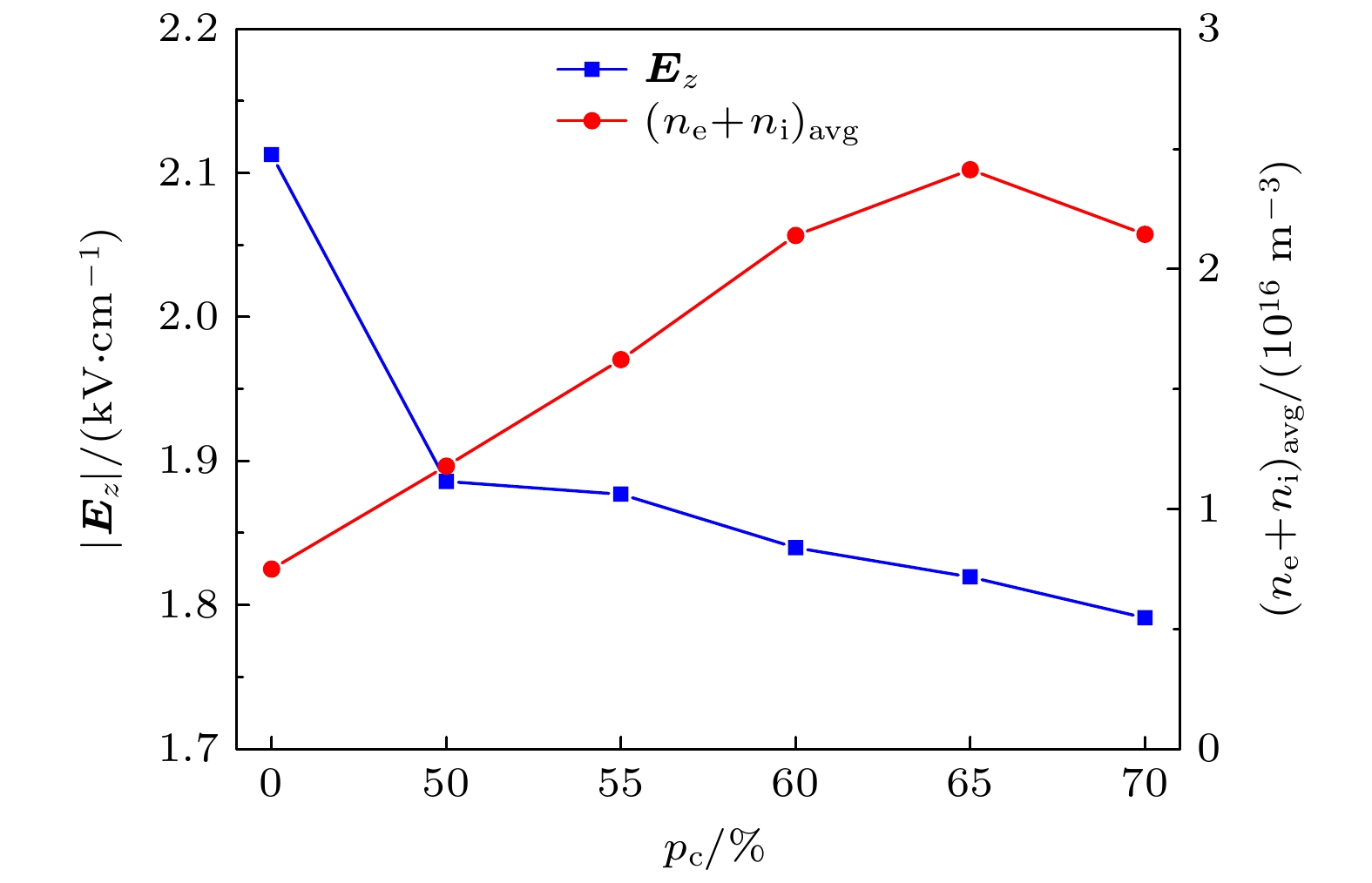
图 15 不同pc下, 放电达到稳态后预电离阶段的轴向平均电场强度|Ez|和轴向平均种子电荷密度(ne + ni)avg
Fig. 15. Axial average electric field |Ez| and axial average seed charge density (ne + ni)avg at pre-ionization stage after discharge reaches steady state under different pc.
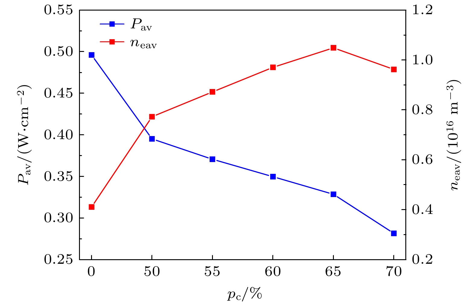
图 16 不同pc下, 放电达到稳态后一个外施电压周期内的时间平均功率密度Pav和时间平均电子密度neav
Fig. 16. Time-averaged power density Pav and time-averaged electron density neav over one period of applied voltage at steady state under different pc.
表 1 等离子体模型的边界条件
Table 1. Boundary conditions of plasma model.
边界 表达式 备注 AB V = Vam 高压电极 GH V = 0 接地 BC, CD, EF, FG $- {\boldsymbol{n}} \cdot D = 0$ 零电荷 DE $- {\boldsymbol{n} } \cdot { {\boldsymbol{\varGamma } }_{\text{e} } } = 0$ 绝缘 $- {\boldsymbol{n} } \cdot { {\boldsymbol{\varGamma } }_{ \text{ε}} } = 0$ DJ, EI Eq. (10)—Eq. (12),
Eq. (14), Eq. (15)介质表面 HIJA ${ {\partial V}/{\partial r} } = 0$ 对称轴  下载: 导出CSV
表 2 模型中输入的初始值
Table 2. Initial parameters applied in model.
参数 初始值 电子数密度/m–3 2.2×10¹³ He+数密度/m–3 1.0×10¹³ $ {\text{He}}_2^ + $数密度/m–3 1.0×10¹³ $ {\text{N}}_2^ + $数密度/m–3 1.0×10¹² $ {\text{N}}_4^ + $数密度/m–3 1.0×10¹² He*摩尔分数 1.0×10⁻⁹ $ {\text{He}}_2^* $摩尔分数 1.0×10⁻⁹ N2摩尔分数 100×10–6 平均电子/eV 4 气体温度/K 300 压强/Torr 760
下载: 导出CSV
-
[1] 梅丹华, 方志, 邵涛 2020 中国电机工程学报 40 1339
Google Scholar
Mei D H, Fang Z, Shao T 2020 Chin. Soc. Elec. Eng. 40 1339
Google Scholar
[2] 戴栋, 宁文军, 邵涛 2017 电工技术学报 32 1
Google Scholar
Dai D, Ning W J, Shao T 2017 Trans. Chin. Elc. Soc. 32 1
Google Scholar
[3] 李和平, 于达仁, 孙文廷, 刘定新, 李杰, 韩先伟, 李增耀, 孙冰, 吴云 2017 高电压技术 42 3697
Google Scholar
Li H P, Yu D L, Sun W T, Liu D X, Li J, Han X W, Li Z Y, Sun B, Wu Y 2017 High Voltage Eng. 42 3697
Google Scholar
[4] Adamovich I, Agarwal S, Ahedo E, et al. 2022 J. Phys. D: Appl. Phys. 55 373001
Google Scholar
[5] Larouss M, Bekeschus S, Bogaerts A, Keidar M, Bogaerts A, Fridman A, Lu B X 2022 IEEE Trans. Radiat. Plasma Med. Sci. 6 127
Google Scholar
[6] Sanito R C, You S J, Wang Y F 2021 J. Environ. Manage. 288 112380
Google Scholar
[7] Laroussi M, Lu X, Keidar M 2017 J. Appl. Phys. 122 020901
Google Scholar
[8] Gaunt L F, Beggs C B, Georghiou G E 2006 IEEE Trans. Plasma Sci. 34 1257
Google Scholar
[9] Ouyang J T, Li B, He F, Dai D 2018 Plasma Sci. Technol. 20 103002
Google Scholar
[10] Fang Z, Qiu Y, Zhang C, Kuffel E 2007 J. Phys. D:Appl. Phys. 40 1401
Google Scholar
[11] Wang Q, Ning W J, Dai D, Zhang Y H, Ouyang J T 2019 J. Phys. D: Appl. Phys. 52 205201
Google Scholar
[12] Zhang Y H, Ning W J, Dai D, Wang Q 2019 Plasma Sources Sci. Technol. 28 075003
Google Scholar
[13] Zhang Y H, Neyts E C, Bogaerts A 2016 J. Phys. Chem. C 120 25923
Google Scholar
[14] Hao Y P, Zheng B, Liu Y G 2014 Phys. Plasmas 21 013503
Google Scholar
[15] Zhang P, Kortshagen U 2006 J. Phys. D: Appl. Phys. 39 153
Google Scholar
[16] Zhang J, Wang Y H, Wang D Z 2015 Phys. Plasmas 22 043517
Google Scholar
[17] Brauer I, Punset C, Purwins H G, Boeuf J P 1999 J. Appl. Phys. 85 7569
Google Scholar
[18] Boeuf J P, Bernecker B, Callegari T, Blanco S, Fournier R 2012 Appl. Phys. Lett. 100 244108
Google Scholar
[19] Zhang Y H, Ning W J, Dai D, Wang Q 2019 Plasma Sci. Technol. 21 074003
Google Scholar
[20] Huang Z M, Hao Y P, Han Y Y, Yang L, Tang L, Liao Y F, Li L C 2017 Phys. Plasmas 24 113506
Google Scholar
[21] Ye Q Z, Wu Y F, Li X W, Chen T, Shao G W 2012 Plasma Sources Sci. Technol. 21 065008
Google Scholar
[22] Motrescu I, Ciolan M A, Sugiyama K, Kawamura N, Nagatsu M 2018 Plasma Sources Sci. Technol. 27 115005
Google Scholar
[23] Wang X X, Luo H Y, Liang Z, Mao T, Ma R L 2006 Plasma Sources Sci. Technol. 15 845
Google Scholar
[24] Brandenburg R 2017 Plasma Sources Sci. Technol. 26 053001
Google Scholar
[25] Heinlin J, Morfill G, Landthaler M, Stolz W, Isbary G, Zimmermann J L, Shimizu T, Karrer S 2010 J. Dtsch. Dermatol. Ges. 8 968
Google Scholar
[26] Buendia J A, Venkattraman A 2015 Europhys. Lett. 112 55002
Google Scholar
[27] Fu Y Y, Zhang P, Verboncoeur J P, Christlieb A J, Wang X X 2018 Phys. Plasmas 25 013530
Google Scholar
[28] Fu Y Y, Zhang P, Verboncoeur J P 2018 Appl. Phys. Lett. 113 054102
Google Scholar
[29] Levko D, Raja L L 2015 J. Appl. Phys. 117 173303
Google Scholar
[30] Go D B, Venkattraman A 2014 J. Phys. D: Appl. Phys. 47 503001
Google Scholar
[31] Venkattraman A, Garg A, Peroulis D, Alexeenko A A 2012 Appl. Phys. Lett. 100 083503
Google Scholar
[32] Cheng H, Liu X, Lu X P, Liu D W 2016 Phys. Plasmas 23 073517
Google Scholar
[33] Cheng H, Xu M Y, Pan S H, Lu X P, Liu D W 2018 Plasma Sci. Technol. 20 044006
Google Scholar
[34] Wang Q, Ning W J, Dai D, Zhang Y H 2019 Plasma Process. Polym. 17 1900182
Google Scholar
[35] Mujahid Z, Korolov I, Liu Y, Mussenbrock T, Schulze J 2022 J. Phys. D: Appl. Phys. 55 495201
Google Scholar
[36] Babaeva N Y, Tian W, Kushner M J 2014 J. Phys. D: Appl. Phys. 47 235201
Google Scholar
[37] Babaeva N Y, Kushner M J 2013 J. Phys. D:Appl. Phys. 46 025401
Google Scholar
[38] Lin A, Biscop E, Gorbanev Y, Smits E, Bogaerts A 2021 Plasma Process. Polym. 19 e2100151
Google Scholar
[39] Zhang Y H, Ning W J, Dai D, Wang Q 2019 Plasma Sources Sci. Technol. 28 104001
Google Scholar
[40] Kong M G, Deng X T 2003 IEEE Trans. Plasma Sci. 31 7
Google Scholar
[41] Fridman G, Friedman G, Gutsol A, Shekhter A B, Vasilets V N, Fridman A 2008 Plasma Process. Polym. 5 503
Google Scholar
[42] Ning W J, Dai D, Li L C 2018 Plasma Sources Sci. Technol. 27 08LT01
Google Scholar
[43] Cheng H, Liu X, Liu D W, Lu X P 2016 High Volt. 1 62
Google Scholar
[44] Lazarou C, Belmonte T, Chiper A S, Georghiou G E 2016 Plasma Sources Sci. Technol. 25 055023
Google Scholar
[45] 力伯曼, 里登伯格 著 (蒲以康等 译) 2018 等离子体放电与材料工艺原理: 第2版 (北京: 电子工业出版社) 第6—7页
Lieberman M A, Lichtenberg A J (translated by Pu Y K, et al.) 2018 Principles of Plasma Discharges and Materials Processing (2nd Ed.) (Beijing: Publishing House of Electronics Industry) pp6–7 (in Chinese)
[46] Lazarou C, Koukounis D, Chiper A S, Costin C, Topala I, Georghiou G E 2015 Plasma Sources Sci. Technol. 24 035012
Google Scholar
[47] Hagelaar G J M, Pitchford L C 2005 Plasma Sources Sci. Technol. 14 722
Google Scholar
[48] Purwins H G, Stollenwerk L 2014 Plasma Phys. Control. Fusion 56 123001
Google Scholar
[49] Ellis H W, Pai R Y, McDaniel E W, Mason E A, Viehland L A 1976 At. Data Nucl. Data Tables. 17 177
Google Scholar
[50] Yan W, Xia Y, Bi Z H, Song Y, Wang D Z, Sosnin E A, Skakun V S, Liu D P 2017 J. Phys. D: Appl. Phys. 50 345201
Google Scholar
[51] Hagelaar G J M 2000 Phys. Rev. E 62 1452
Google Scholar
[52] Motz H, Wise H 1960 J. Chem. Phys. 32 1893
Google Scholar
[53] Bilici M A, Haase J R, Boyle C R, Go D B, Sankaran R M 2016 J. Appl. Phys. 119 223301
Google Scholar
[54] Boeuf J P, Yang L L, Pitchford L C 2013 J. Phys. D:Appl. Phys. 46 015201
Google Scholar
[55] Petra C G, Schenk O, Anitescu M 2014 Comput. Sci. Eng. 16 32
Google Scholar
[56] Li B, Dong L F, Zhang C, Shen Z K, Zhang X P 2014 J. Phys. D: Appl. Phys. 47 055205
Google Scholar
[57] Huang Z M, Hao Y P, Yang L, Han Y X, Li L C 2015 Phys. Plasmas 22 123519
Google Scholar
[58] Ning W J, Dai D, Zhang Y H, Hao Y P, Li L C 2017 Phys. Plasmas 24 073509
Google Scholar
[59] Golubovskii Y B, Maiorov V A, Behnke J, Behnke J F 2003 J. Phys. D: Appl. Phys. 36 39
Google Scholar
[60] Lee D, Park J M, Hong S H, Kim Y 2005 IEEE Trans. Plasma Sci. 33 949
Google Scholar
[61] Jiang W M, Tang J, Wang Y S, Zhao W, Duan Y X 2013 Phys. Plasmas 20 073509
Google Scholar
[62] Wang Q, Zhou X Y, Dai D, Huang Z, Zhang D M 2021 Plasma Sources Sci. Technol. 30 05LT01
Google Scholar


 下载:
下载:
计量
- 文章访问数: 1822
- PDF下载量: 48
- 被引次数: 0
