


-
利用正、负磁致伸缩系数材料(Terfenol-D, Ni)对相同应变的响应差异, 提出了一种基于异质多铁结构全局应变时钟的纳磁体择多逻辑门, 设计了“高应力启动-低应力计算”的两步择多计算模式, 使用MuMax3微磁学仿真软件建立了该器件的微磁学模型, 并研究了其能量演化情况和周期能耗. 仿真结果表明: 异质多铁结构全局应变时钟纳磁体择多逻辑门能够成功地对任意的3端输入组合连续执行择多计算; 应用两步择多计算模式, 该器件计算正确率可达100%, 其执行连续计算的周期为2.75 ns, 周期能耗约64 aJ. 研究发现: 应力各向异性能和偶极子耦合能变化引起的能量势阱变化是决定该器件磁化动力学行为的主要原因. 本文研究结果可为纳米磁逻辑电路的设计提供重要指导.
In the post-Moore era, nanomagnetic logic circuits have shown great potential to replace complementary metal oxide semiconductor (CMOS) circuits. A majority logic gate, as the core of a nanomagnetic logic circuit, is equivalent to the inverter in the CMOS circuit. A nanomagnetic logic majority gate generally has four nanomagnets arranged in a “T” shape. The nanomagnets in the three corners of the “T” (I1, I2, I3) are the three inputs, and the middle nanomagnet is the output (O). This paper proposes a nanomagnet majority logic gate based on the global strain clock of heterogeneous multiferroic structure, by utilizing the difference in response to the same strain between positive magnetostrictive coefficient material (Terfenol-D) and negative magnetostrictive coefficient material (Ni). From bottom to top, the device is mainly composed of a silicon substrate, a piezoelectric layer, and four elliptical cylindrical nanomagnets. PMN-PT is used as the piezoelectric layer’s material, and three Ni-based nanomagnets (I1, I2, and I3) are utilized as input, while Terfenol-D is used as the material for the output nanomagnet (O). Besides, a two-step calculation mode of “high-stress start-low-stress calculation” is designed, that is, the O is first switched to the “Null” with a stress of –30 MPa, and then the stress decreases to –15 MPa, so that the O can realize majority calculation under the coupling of I1, I2, and I3. The micromagnetic simulation software MuMax3 is adopted to simulate the performance of the device. The results reveal that the device can successfully perform continuous majority calculation through any three-terminal input combination. By using the two-step calculation mode, the calculation accuracy of the device can reach 100%, its cycle of continuous calculation is 2.75 ns, and the cycle energy consumption is about 64 aJ. It is found that the change of energy potential well, caused by the change of stress anisotropy energy and dipole coupling energy, is the main reason that determines the magnetization dynamic behavior of the device. Therefore, the results of this paper can provide important guidance for designing nanomagnetic logic circuits. -
Keywords:
- majority logic gate /
- multiferroic nanomagnets /
- nanomagnet logic /
- heterogeneous multiferroic structure
[1] DeBenedictis, P E 2017 Computer 50 72
 Google Scholar
[2] Liu S L, Hu X S, Nahas J J, Niemier M T, Porod W, Bernstein G H 2011 IEEE Trans. Nanotechnol. 10 757
Google Scholar
[3] Gypens P, Leliaert J, Van Waeyenberge B 2018 Phys. Rev. Appl. 9 034004
Google Scholar
[4] Gonelli M, Fin S, Carlotti G, Dey H, Csaba G, Porod W, Bernstein G H, Bisero D 2018 J. Magn. Magn. Mater. 460 432
Google Scholar
[5] Imre A, Csaba G, Ji L, Orlov A, Bernstein G, Porod W 2006 Science 311 205
Google Scholar
[6] Orlov A, Imre A, Csaba G, Ji L, Porod W, Bernstein G 2008 J. Nanoelectron. Optoelectron. 3 55
Google Scholar
[7] 刘嘉豪, 杨晓阔, 危波, 李成, 张明亮, 李闯, 董丹娜 2019 物理学报 68 017501
Google Scholar
Liu J H, Yang X K, Wei B, Li C, Zhang M L, Li C, Dong D N 2019 Acta Phys. Sin. 68 017501
Google Scholar
[8] Carlton D B, Lambson B, Scholl A, Young A T, Dhuey S D, Ashby P D, Tuchfeld E, Bokor J 2011 IEEE Trans. Nanotechnol. 10 1401
Google Scholar
[9] Gu Z, Nowakowski M E, Carlton D B, Storz R, Im M Y, Hong J, Chao W, Lambson B, Bennett P, Alam M T, Marcus M A, Doran A, Young A, Scholl A, Fischer P, Bokor J 2015 Nat. Commun. 6 6466
Google Scholar
[10] 杨晓阔, 张斌, 崔焕卿, 李伟伟, 王森 2016 物理学报 65 237502
Google Scholar
Yang X K, Zhang B, Cui H Q, Li W W, Wang S 2016 Acta Phys. Sin. 65 237502
Google Scholar
[11] Atulasimha J, Bandyopadhyay S 2010 Appl. Phys. Lett. 97 173105
Google Scholar
[12] 张楠, 张保, 杨美音, 蔡凯明, 盛宇, 李予才, 邓永城, 王开友 2017 物理学报 66 027501
Google Scholar
Zhang N, Zhang B, Yang M Y, Cai K M, Sheng Y, Li Y C, Deng Y C, Wang K Y 2017 Acta Phys. Sin. 66 027501
Google Scholar
[13] Alam M T, Kurtz S J, Siddiq M A J, Niemier M T, Bernstein G H, Hu X S, Porod W 2011 IEEE Trans. Nanotechnol. 11 273
Google Scholar
[14] 张明亮, 蔡理, 杨晓阔, 秦涛, 刘小强, 冯朝文, 王森 2014 物理学报 63 227503
Google Scholar
Zhang M L, Cai L, Yang X K, Qin T, Liu X Q, Feng C W, Wang S 2014 Acta Phys. Sin. 63 227503
Google Scholar
[15] Bhowmik D, You L, Salahuddin S 2014 Nat. Nanotechnol. 9 59
Google Scholar
[16] Suh D I, Bae G Y, Oh H S, Park W 2015 J. Appl. Phys. 117 17D714
Google Scholar
[17] Sengupta A, Choday S H, Kim Y, Roy K 2015 Appl. Phys. Lett. 106 143701
Google Scholar
[18] Ostwal V, Debashis P, Faria R, Chen Z H, Appenzeller J 2018 Sci. Rep. 8 16689
Google Scholar
[19] Liu M, Zou Q, Ma C R, Collins G, Mi S B, Jia C L, Guo H M, Gao H J, Chen C L 2014 ACS Appl. Mater. Interfaces 6 8526
Google Scholar
[20] Cui H Q, Cai L, Yang X K, Wang S, Feng C W, Xu L, Zhang M L 2017 J. Phys. D:Appl. Phys. 50 285001
Google Scholar
[21] Yuan J H, Yang X K, Wei B, Chen Y B, Cui H Q, Liu J H, Dou S Q, Song M X, Fei L 2023 Phys. Rev. Appl. 19 014003
Google Scholar
[22] Bandyopadhyay S, Atulasimha J, Barman A 2021 Appl. Phys. Rev. 8 041323
Google Scholar
[23] 危波, 蔡理, 杨晓阔, 李成 2017 物理学报 66 217501
Google Scholar
Wei B, Cai L, Yang X K, Li C 2017 Acta Phys. Sin. 66 217501
Google Scholar
[24] Yilmaz Y, Mazumder P 2013 IEEE Trans. Very Large Scale Integr. VLSI Syst. 21 1181
Google Scholar
[25] D’Souza N, Salehi Fashami M, Bandyopadhyay S, Atulasimha J 2016 Nano Lett. 16 1069
Google Scholar
[26] Chen Y B, Yang X K, Wei B, Cui H Q, Song M X 2020 IEEE Access 8 77802
Google Scholar
[27] Zhang J, Lee W K, Tu R, Rhee D, Zhao R, Wang X, Liu X, Hu X, Zhang X, Odom T, Yan M 2021 Nano Lett. 21 5430
Google Scholar
[28] Chen A T, Piao H G, Zhang C H, Ma X P, Algaidi H, Ma Y C, Li Y, Zheng D X, Qiu Z D, Zhang X X 2023 Mater. Horiz. DOI: 10.1039/d3mh00378
[29] Khojah R, Xiao Z, Panduranga M K, Bogumil M, Wang Y, Goiriena-Goikoetxea M, Chopdekar R V, Bokor J, Carman G P, Candler R N, Di Carlo D 2021 Adv. Mater. 33 2006651
Google Scholar
[30] Huang B, Zhu W, Hua L, Wang J, Guo Y 2022 Curr. Appl. Phys. 41 139
Google Scholar
[31] Jin T L, Hao L, Cao J W, Liu M F, Dang H G, Wang Y, Wu D P, Bai J M, Wei F L 2014 Appl. Phys. Express 7 043002
Google Scholar
[32] Pathak P, Mallick D 2022 IEEE Trans. Magn. 58 3401406
Google Scholar
[33] Roy K, Bandyopadhyay S, Atulasimha J 2011 Phys. Rev. B 83 224412
Google Scholar
[34] Bhattacharya D, Al-Rashid M M, D'Souza N, Bandyopadhyay S, Atulasimha J 2017 Nanotechnology 28 015202
Google Scholar
[35] Chen Y B, Wei B, Yang X K, Liu J H, Li J, Cui H Q, Li C, Song M X 2020 J. Magn. Magn. Mater. 514 167216
Google Scholar
[36] Beleggia M, Graef M D, Millev Y T, Goode D A, Rowlands G 2005 J. Phys. D: Appl. Phys. 38 3333
Google Scholar
[37] Vacca M, Graziano M, Crescenzo L D, Chiolerio A, Lamberti A, Balma D, Canavese G, Celegato F, Enrico E, Tiberto P, Boarino L, Zamboni M 2014 IEEE Trans. Nanotechnol. 13 963
Google Scholar
[38] Fidler J, Schrefl T 2000 J. Phys. D:Appl. Phys. 33 R135
Google Scholar
[39] Boechler G P, Whitney J M, Lent C S, Orlov A O, Snider G L 2010 Appl. Phys. Lett. 97 103502
Google Scholar
-

图 1 椭圆柱体纳磁体布尔逻辑编码方式
Fig. 1. Cylindrical elliptical nanomagnet logic coding for Booleans.

图 2 NMLC组件 (a)择多逻辑门 (b) 铁磁耦合互连线; (c) 反铁磁耦合互连线
Fig. 2. NMLC Components: (a) Majority gate; (b) ferromagnetic coupling interconnect wire; (c) anti-ferromagnetic coupling interconnect wire.
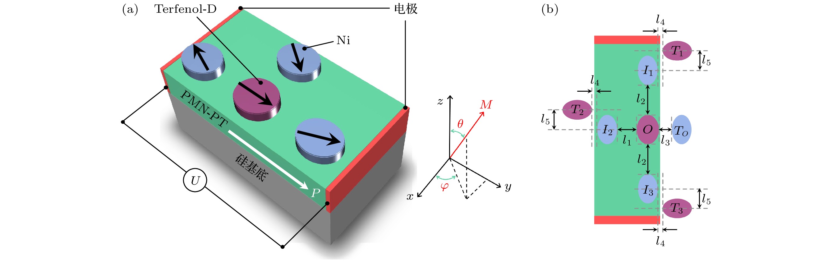
图 3 异质多铁结构全局应变时钟纳磁体择多逻辑门 (a) 立体结构; (b) 俯视图
Fig. 3. Nanomagnets majority gate based on global strain clock of heterogeneous multiferroic structure: (a) Stereo structure; (b) top view.
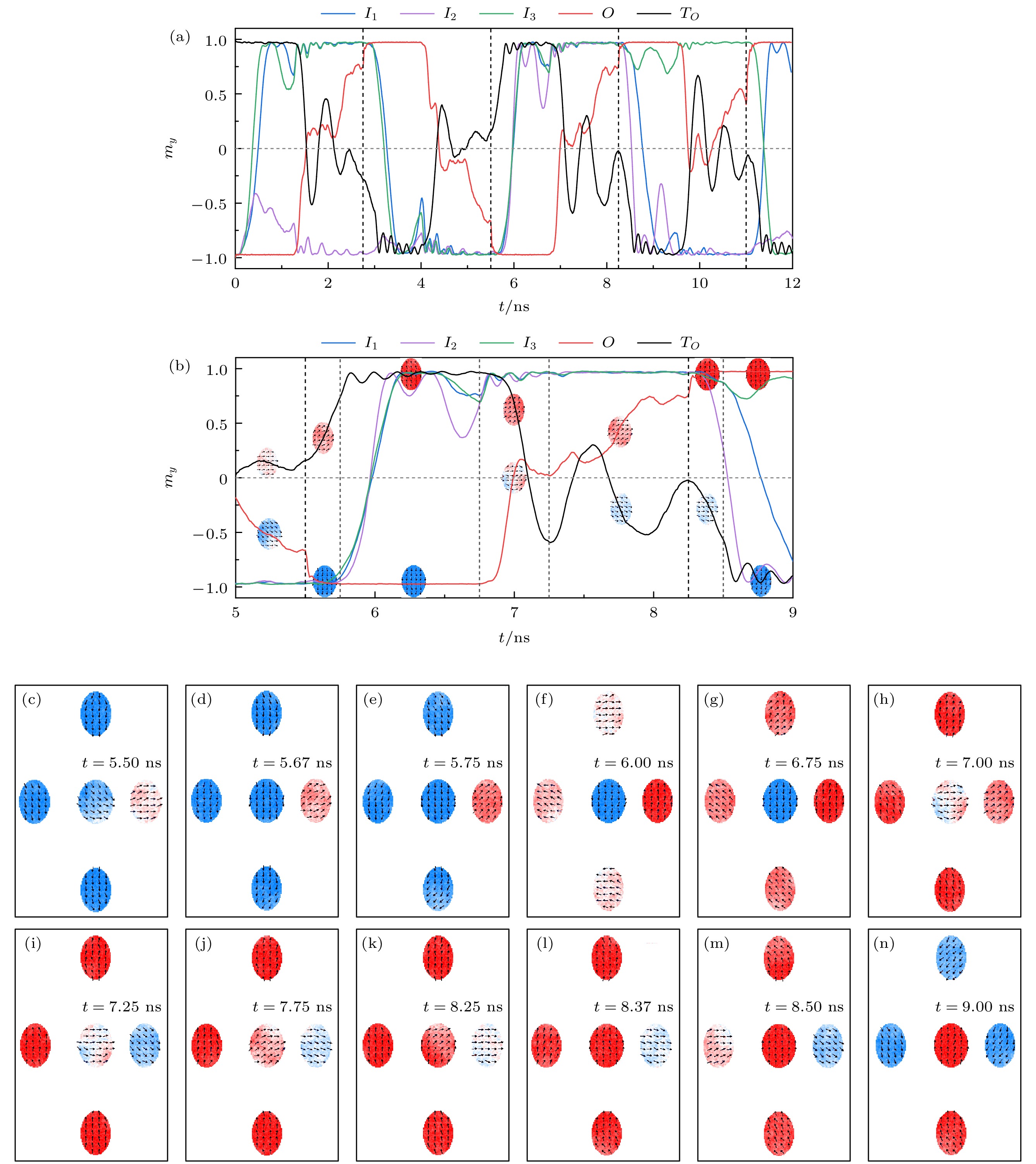
图 5 异质多铁择多门连续工作磁化动态过程 (a) 初始态000, 输入依次为“101”, “000”, “111”和“001”时的磁化动态曲线; (b) 第3周期, 即“0000”条件下输入“111”择多计算详细磁化动态过程; (c)—(n) 异质多铁择多门中纳磁体磁化状态
Fig. 5. Magnetization dynamic process of the majority gate continuously work: (a) The dynamics of the magnetization curve when the initial state is “000” and the input is “101”, “000”, “111”, “001” in sequence; (b) the detailed magnetization dynamic process calculated at the third cycle, i.e., at input “111” under “0000” conditions; (c)–(n) magnetization states of nanomagnets in the majority gate.

图 6 纳磁体能量势垒方向及其能量势阱方向 (a) 能量势阱附近的单侧波动; (b) 跨越短轴的双侧波动; (c) 施加极性相反的电压时或者撤去电压后, 磁矩进动的方向
Fig. 6. Nanomagnet’s energy potential well direction and its energy barrier direction: (a) Unilateral fluctuations near the energy potential well; (b) bilateral fluctuations across the short axis; (c) the direction of the magnetic moment progresses when a voltage of opposite polarity is applied or when the voltage is removed.
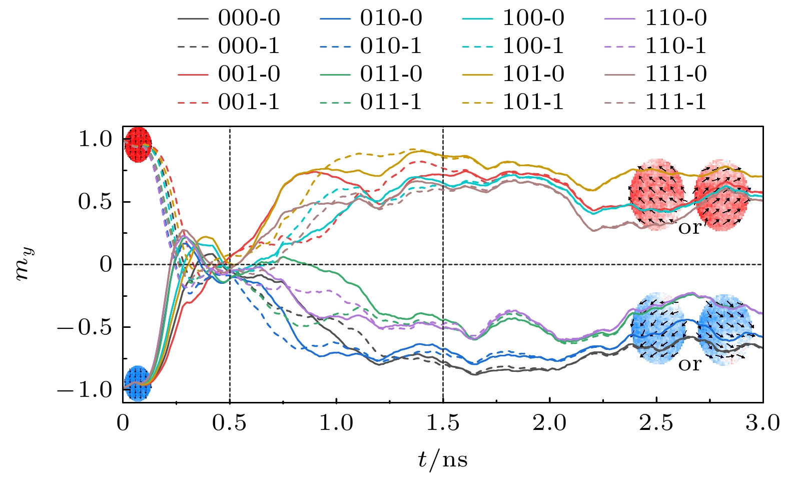
图 7 异质多铁择多门所有择多计算情形下, O的磁矩的动态变化. 0—0.5 ns, 施加–30 MPa应力; 0.5—3 ns, 施加–15 MPa应力. “000-0”代表初始状态为: I1I2I3 = 000, O = 0时O的磁矩的动态变化曲线
Fig. 7. Dynamic variation of the magnetic moment of O for all calculation cases of the logic gate. 0–0.5 ns, –30 MPa stress applied; 0.5–3 ns, –15 MPa stress applied. “000-0” represents the dynamic variation of the magnetic moment of O when the initial state is: I1I2I3 = 000 and O = 0.

图 8 信息传出逻辑门的所有情形下, O和TO的磁矩的动态变化. 全局应变时钟: 0—0.5 ns, 施加–30 MPa应力; 0.5—1.5 ns, 施加–15 MPa应力; 1.5—2.5 ns, 施加250 MPa应力. TO控制时钟: 0—2.5 ns, 施加300 MPa应力. “000-0”代表初始状态为: I1I2I3 = 000且O = 0时, O的磁矩的动态曲线; “0000-0”代表初始状态为: I1I2I3O = 0000且TO = 0时, TO的磁矩的动态曲线
Fig. 8. Dynamic variation of the magnetic moments of O and TO for all cases of information passing out of the logic gate. Global strain clock: 0–0.5 ns, –30 MPa stress applied; 0.5–1.5 ns, –15 MPa stress applied; 1.5–2.5 ns, 250 MPa stress applied. TO control clock: 0–2.5 ns, 300 MPa stress applied. “000-0” represents the dynamic curve of the magnetic moment of O when the initial state is: I1I2I3 = 000 and O = 0; “0000-0” represents the dynamic curve of the magnetic moment of TO when the initial state is: I1I2I3O = 0000 and TO = 0.

图 9 异质多铁择多门连续计算时的能量演化 (a) 全局应变时钟; (b)—(f) I1, I2, I3, O及TO的能量密度; (g) TO 控制时钟
Fig. 9. Energy evolution during continuous computation of the logic gate: (a) Global strain clock; (b)–(f) energy density of I1, I2, I3, O and TO; (g) control the clock of TO.
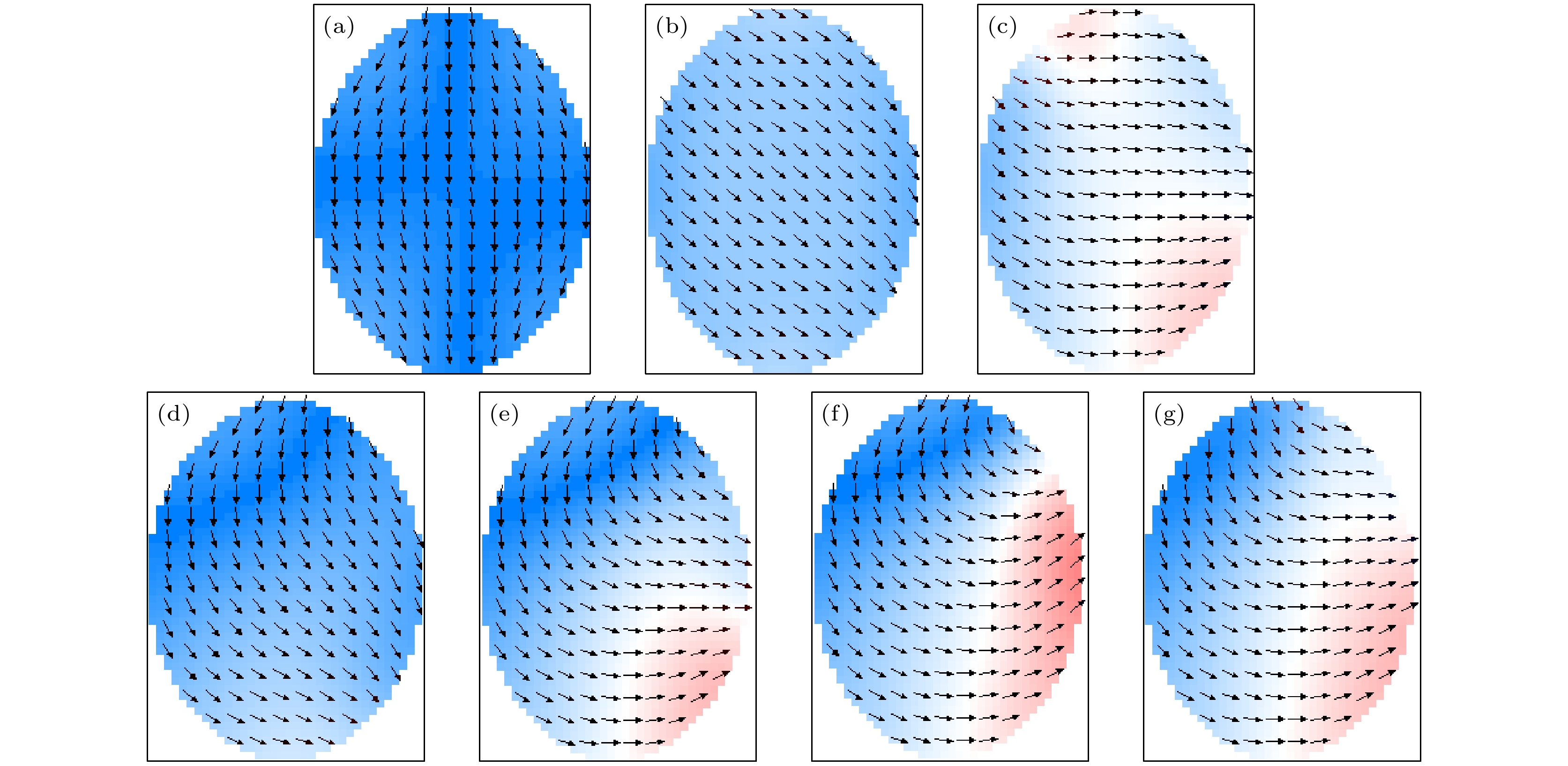
图 10 纳磁体磁矩偏转90° (a)—(c) 一致的单畴态偏转; (a), (d)—(g), (c) 非一致的“C”形态偏转
Fig. 10. Nanomagnet magnetic moment switching 90°: (a)–(c) Uniform single-domain Switching; (a), (d)–(g), (c) non-uniform “C” form Switching.
表 1 器件尺寸及布局参数
Table 1. Parameters of the device size and layout.
名称 尺寸/nm 名称 尺寸/nm 所有纳磁体长轴 a 120 I2与O间距 l1 80 所有纳磁体厚度 h 10 I1, I3与O间距 l2 120 O的短轴 b1 90 TO与O间距 l3 50 其余纳磁体短轴 b2 80 T1, T2, T3分别
与I2, I2, I3
水平间距 l420 压电层长度 ly 700 T1, T2, T 3分别
与I2, I2, I3
垂直中心距 l580 压电层宽度 lx 265 压电层厚度 lz 100  下载: 导出CSV
表 2 纳磁体材料参数
Table 2. Material parameters of nanomagnets.
Terfenol-D Ni 杨氏模量 Y/1010 Pa 8 21.4 磁致伸缩系数 λS/10–4 +6 –0.2 吉尔伯特阻尼系数 α 0.1 0.045 饱和磁化强度 MS/(105 A·m–1) 8 4.85 交换作用常数 A/(10–11 J·m–1) 0.9 1.05
下载: 导出CSV
表 3 应变时钟参数
Table 3. Strain clock parameters.
时钟参数 数值/MPa 时钟参数 数值/ns σ+ 250 t1 1.25 σH– –30 t2 1.75 σL– –15 t3 2.75 $ \sigma_{T_{O} } $ 300 t4 3
下载: 导出CSV
-
[1] DeBenedictis, P E 2017 Computer 50 72
Google Scholar
[2] Liu S L, Hu X S, Nahas J J, Niemier M T, Porod W, Bernstein G H 2011 IEEE Trans. Nanotechnol. 10 757
Google Scholar
[3] Gypens P, Leliaert J, Van Waeyenberge B 2018 Phys. Rev. Appl. 9 034004
Google Scholar
[4] Gonelli M, Fin S, Carlotti G, Dey H, Csaba G, Porod W, Bernstein G H, Bisero D 2018 J. Magn. Magn. Mater. 460 432
Google Scholar
[5] Imre A, Csaba G, Ji L, Orlov A, Bernstein G, Porod W 2006 Science 311 205
Google Scholar
[6] Orlov A, Imre A, Csaba G, Ji L, Porod W, Bernstein G 2008 J. Nanoelectron. Optoelectron. 3 55
Google Scholar
[7] 刘嘉豪, 杨晓阔, 危波, 李成, 张明亮, 李闯, 董丹娜 2019 物理学报 68 017501
Google Scholar
Liu J H, Yang X K, Wei B, Li C, Zhang M L, Li C, Dong D N 2019 Acta Phys. Sin. 68 017501
Google Scholar
[8] Carlton D B, Lambson B, Scholl A, Young A T, Dhuey S D, Ashby P D, Tuchfeld E, Bokor J 2011 IEEE Trans. Nanotechnol. 10 1401
Google Scholar
[9] Gu Z, Nowakowski M E, Carlton D B, Storz R, Im M Y, Hong J, Chao W, Lambson B, Bennett P, Alam M T, Marcus M A, Doran A, Young A, Scholl A, Fischer P, Bokor J 2015 Nat. Commun. 6 6466
Google Scholar
[10] 杨晓阔, 张斌, 崔焕卿, 李伟伟, 王森 2016 物理学报 65 237502
Google Scholar
Yang X K, Zhang B, Cui H Q, Li W W, Wang S 2016 Acta Phys. Sin. 65 237502
Google Scholar
[11] Atulasimha J, Bandyopadhyay S 2010 Appl. Phys. Lett. 97 173105
Google Scholar
[12] 张楠, 张保, 杨美音, 蔡凯明, 盛宇, 李予才, 邓永城, 王开友 2017 物理学报 66 027501
Google Scholar
Zhang N, Zhang B, Yang M Y, Cai K M, Sheng Y, Li Y C, Deng Y C, Wang K Y 2017 Acta Phys. Sin. 66 027501
Google Scholar
[13] Alam M T, Kurtz S J, Siddiq M A J, Niemier M T, Bernstein G H, Hu X S, Porod W 2011 IEEE Trans. Nanotechnol. 11 273
Google Scholar
[14] 张明亮, 蔡理, 杨晓阔, 秦涛, 刘小强, 冯朝文, 王森 2014 物理学报 63 227503
Google Scholar
Zhang M L, Cai L, Yang X K, Qin T, Liu X Q, Feng C W, Wang S 2014 Acta Phys. Sin. 63 227503
Google Scholar
[15] Bhowmik D, You L, Salahuddin S 2014 Nat. Nanotechnol. 9 59
Google Scholar
[16] Suh D I, Bae G Y, Oh H S, Park W 2015 J. Appl. Phys. 117 17D714
Google Scholar
[17] Sengupta A, Choday S H, Kim Y, Roy K 2015 Appl. Phys. Lett. 106 143701
Google Scholar
[18] Ostwal V, Debashis P, Faria R, Chen Z H, Appenzeller J 2018 Sci. Rep. 8 16689
Google Scholar
[19] Liu M, Zou Q, Ma C R, Collins G, Mi S B, Jia C L, Guo H M, Gao H J, Chen C L 2014 ACS Appl. Mater. Interfaces 6 8526
Google Scholar
[20] Cui H Q, Cai L, Yang X K, Wang S, Feng C W, Xu L, Zhang M L 2017 J. Phys. D:Appl. Phys. 50 285001
Google Scholar
[21] Yuan J H, Yang X K, Wei B, Chen Y B, Cui H Q, Liu J H, Dou S Q, Song M X, Fei L 2023 Phys. Rev. Appl. 19 014003
Google Scholar
[22] Bandyopadhyay S, Atulasimha J, Barman A 2021 Appl. Phys. Rev. 8 041323
Google Scholar
[23] 危波, 蔡理, 杨晓阔, 李成 2017 物理学报 66 217501
Google Scholar
Wei B, Cai L, Yang X K, Li C 2017 Acta Phys. Sin. 66 217501
Google Scholar
[24] Yilmaz Y, Mazumder P 2013 IEEE Trans. Very Large Scale Integr. VLSI Syst. 21 1181
Google Scholar
[25] D’Souza N, Salehi Fashami M, Bandyopadhyay S, Atulasimha J 2016 Nano Lett. 16 1069
Google Scholar
[26] Chen Y B, Yang X K, Wei B, Cui H Q, Song M X 2020 IEEE Access 8 77802
Google Scholar
[27] Zhang J, Lee W K, Tu R, Rhee D, Zhao R, Wang X, Liu X, Hu X, Zhang X, Odom T, Yan M 2021 Nano Lett. 21 5430
Google Scholar
[28] Chen A T, Piao H G, Zhang C H, Ma X P, Algaidi H, Ma Y C, Li Y, Zheng D X, Qiu Z D, Zhang X X 2023 Mater. Horiz. DOI: 10.1039/d3mh00378
[29] Khojah R, Xiao Z, Panduranga M K, Bogumil M, Wang Y, Goiriena-Goikoetxea M, Chopdekar R V, Bokor J, Carman G P, Candler R N, Di Carlo D 2021 Adv. Mater. 33 2006651
Google Scholar
[30] Huang B, Zhu W, Hua L, Wang J, Guo Y 2022 Curr. Appl. Phys. 41 139
Google Scholar
[31] Jin T L, Hao L, Cao J W, Liu M F, Dang H G, Wang Y, Wu D P, Bai J M, Wei F L 2014 Appl. Phys. Express 7 043002
Google Scholar
[32] Pathak P, Mallick D 2022 IEEE Trans. Magn. 58 3401406
Google Scholar
[33] Roy K, Bandyopadhyay S, Atulasimha J 2011 Phys. Rev. B 83 224412
Google Scholar
[34] Bhattacharya D, Al-Rashid M M, D'Souza N, Bandyopadhyay S, Atulasimha J 2017 Nanotechnology 28 015202
Google Scholar
[35] Chen Y B, Wei B, Yang X K, Liu J H, Li J, Cui H Q, Li C, Song M X 2020 J. Magn. Magn. Mater. 514 167216
Google Scholar
[36] Beleggia M, Graef M D, Millev Y T, Goode D A, Rowlands G 2005 J. Phys. D: Appl. Phys. 38 3333
Google Scholar
[37] Vacca M, Graziano M, Crescenzo L D, Chiolerio A, Lamberti A, Balma D, Canavese G, Celegato F, Enrico E, Tiberto P, Boarino L, Zamboni M 2014 IEEE Trans. Nanotechnol. 13 963
Google Scholar
[38] Fidler J, Schrefl T 2000 J. Phys. D:Appl. Phys. 33 R135
Google Scholar
[39] Boechler G P, Whitney J M, Lent C S, Orlov A O, Snider G L 2010 Appl. Phys. Lett. 97 103502
Google Scholar

 下载:
下载:

计量
- 文章访问数: 1424
- PDF下载量: 36
- 被引次数: 0
