


-
金属纳米颗粒低聚体不仅具有等离激元共振效应实现光场亚波长范围内的局域化和增强, 还可以通过泄漏光场相互干涉实现法诺共振和连续态中的束缚态, 从而使得电磁场更强的局域和增强. 本文采用金纳米低聚体超构表面作为石墨烯/硅近红外探测器的天线, 实现了光响应度2倍的增强; 通过调节纳米金属低聚体间夹角, 发现当该夹角为40°时, 光电流达到最大值, 对应法诺共振最大的透射率, 此时天线不仅汇聚光场能量还定向发射给探测器; 当该夹角为20°时, 光电流出现一个低谷, 此时能量局域于低聚体内, 金属损耗减弱了等离激元增强效果. 该工作通过时域有限差分法仿真和实验相结合研究了低聚体超构表面光电耦合效率的动态过程, 为提高光电探测效率提供了一种重要的途径.Infrared imaging chips are crucial for a broad range of military, medicine and biology applications. Although silicon detectors’ on-chip integration technology is matured, their low absorption in near-infrared light results in poor infrared photocurrent response. To increase the photodetector absorption efficiency, antenna-like metal nanoparticles have been widely adopted due to their plasmon resonance effects. Oligomer nanoparticles, including quaternary nanoparticles, exhibit plasmon resonance effects that localize and enhance the light field in a sub-wavelength range. Furthermore, they can interfere with each other to achieve Fano resonance and bound state in continuity, resulting in a stronger localization and enhancement of the electromagnetic field. In this study an array of gold quaternary nanoparticle oligomers is used as the antenna for a graphene/SOI (with 1 μm silicon) heterojunction near-infrared detector. Each oligomer consists of four gold squares, each with a size of 250 nm, forming two pairs of dipoles similar to the orbital hybridization of hydrogen atoms. This thus results in a multi-body coupling structure with bonding state and anti-bonding state. The antenna array parameters, such as the periodic constant, gap between nanoparticles, and angle (θ) between the oligomers, are meticulously adjusted. The optimized device is characterized by using photocurrent and photocurrent mapping, achieving a 2-fold enhancement in photoresponsivity with the maximum value at θ ~ 40°. Notably, a consistent dip in photocurrents is observed for different periods or gap arrays when the angle theta is 20°. The simulation is conducted by using finite-difference time-domain (FDTD), revealing the emergence of Fano-like resonance in the transmittance spectra of the array at approximately 850 nm. The interference caused by the strongly coupling system to the plane coupled leakage field and the nanoparticle plasmon mode results in the formation of a new discrete leakage mode, i.e. the Fano-like resonance. The antenna helps to concentrate and emit the light field energy directionally to the detector, while there is a trade-off between the loss caused by nanoparticles absorption and the leakage energy. The photocurrent reaches a minimal point at a theta angle of 20° angle. At this point, the energy is localized in the oligomers, and the metal absorption loss weakens the plasmon enhancement effect. These findings are further supported by the simulation results of electric field and Poynting vector distribution. These findings indicate an important and promising way to enhance the photo detection efficiency via nanostructured plasmonic antenna.
-
Keywords:
- nano-antenna /
- plasmonic /
- silicon infrared photodetector /
- graphene
[1] Ijaz S, Rana A S, Ahmad Z, Zubair M, Massoud Y, Mehmood M Q 2022 Adv. Devices Instrument. 2022 9861078
 Google Scholar
[2] Zhang L, Cui T J 2021 Research 2021 9802673
Google Scholar
[3] Xing H, Fan J, Lu D, Gao Z, Shum P P, Cong L 2022 Adv. Devices Instrument. 2022 9852503
Google Scholar
[4] Fang M, Tan X, Liu Z, Hu B, Wang X 2021 Research 2021 9794329
Google Scholar
[5] Maier S A 2007 Plasmonics: Fundamentals and Applications (Berlin, Heideberg: Springer) pp5–19
[6] Mirin N A, Bao K, Nordlander P 2009 J. Phys. Chem. A 113 4028
Google Scholar
[7] Gallinet B, Martin O J F 2011 ACS Nano 5 8999
Google Scholar
[8] Luk'yanchuk B, Zheludev N I, Maier S A, Halas N J, Nordlander P, Giessen H, Chong C T, 2010 Nat. Mater. 9 707
Google Scholar
[9] Hsu C W, Zhen B, Stone A D, Joannopoulos J D, Soljačić M 2016 Nat. Rev. Mater. 1 16048
Google Scholar
[10] Liang Y, Koshelev K, Zhang F, Lin H, Lin S, Wu J, Jia B, Kivshar Y 2020 Nano Lett. 20 635
Google Scholar
[11] 闫梦, 孙珂, 宁廷银, 赵丽娜, 任莹莹, 霍燕燕 2023 物理学报 72 044202
Google Scholar
Yan M, Sun K, Ning T Y, Zhao L N, Ren Y Y, Huo Y Y 2023 Acta Phys. Sin. 72 044202
Google Scholar
[12] Wu N X, Ma H B, Chen H S, Qian H L 2021 Prog. Electromagn. Res. 172 23
Google Scholar
[13] Liu L L, Zhuo L 2022 Prog. Electromagn. Res. 173 93
Google Scholar
[14] Rogers C, Piggott A Y, Thomson D J, Wiser R F, Opris I E, Fortune S A , Compston A J, Gondarenko A, Meng F, Che X, Reed G T, Nicolaescu R 2021 Nature 590 256
Google Scholar
[15] Fossum E R 1997 IEEE T. Electron Dev. 44 1689
Google Scholar
[16] 李龙珍, 姚旭日, 刘雪峰, 俞文凯, 翟光杰 2014 物理学报 63 224201
Google Scholar
Li L Z, Yao X R, Liu X F, Yu W K, Zhai G J 2014 Acta Phys. Sin. 63 224201
Google Scholar
[17] 吴国安, 罗林保 2018 物理 47 137
Google Scholar
Wu G A, Luo L B 2018 Physics 47 137
Google Scholar
[18] 陈浩, 张晓霞, 王鸿, 姬月华 2018 物理学报 67 118101
Google Scholar
Chen H, Zhang X X, Wang H, Ji Y H 2018 Acta Phys. Sin. 67 118101
Google Scholar
[19] 龙弯, 许中杰 2015 激光与光电子学进展 52 26
Google Scholar
Long W, Xu Z J 2015 Laser Optoelectron. Prog. 52 26
Google Scholar
[20] Nordlander P, Oubre C, Prodan E, Li K, Stockman M I 2004 Nano Lett. 4 899
Google Scholar
[21] Wang H, Brandl D W, Nordlander P, Halas N J 2007 Accounts Chem. Res. 40 53
Google Scholar
[22] Tang B, Jia Z, Huang L, Su J, Jiang C 2021 IEEE J. Sel. Top. Quant. 27 1
Google Scholar
[23] Li L F, Wang J Z, Kang L, Liu W, Yu L, Zheng B J, Brongersma M L, Werner D H, Lan S F, Shi Y, Xu Y, Wang X M 2020 ACS Nano 14 16634
Google Scholar
[24] Goykhman I, Sassi U, Desiatov B, Mazurski N, Milana S, Fazio D, Eiden A, Khurgin J, Shappir J, Levy U, Ferrari A C 2016 Nano Lett. 16 3005
Google Scholar
[25] Wang X, Cheng Z, Xu K, Tsang H K, Xu J B 2013 Nat. Photonics 7 888
Google Scholar
[26] Xu S, Sayanskiy A, Kupriianov, Tuz V R, Kapitanova P, Sun H B, Han W, Kivshar Y S 2019 Adv. Opt. Mater. 7 1801166
Google Scholar
[27] Zhang G, Lan C, Gao R, Wen Y, Zhou J 2019 Adv. Theory Simulat. 2 1900123
Google Scholar
[28] Russell K J, Hu E L 2010 Appl. Phys. Lett. 97 163115
Google Scholar
[29] Wu Z Q, Yang J L, Manjunath N K, Zhang Y J, Feng S R, Lu Y H, Wu J H, Zhao W W, Qiu C Y, Li J F, Lin S S 2018 Adv. Mater. 30 1706527
Google Scholar
-

图 1 纳米天线器件制备流程示意图 (a) SOI上刻蚀出硅岛; (b)蒸镀金属接触电极; (c)硅岛上制备纳米天线阵列; (d)转移石墨烯薄膜; (e)器件显微镜照片
Fig. 1. Device with antenna fabrication process: (a) Si island fabrication from SOI substrate; (b) electrodes deposition with EBE technique; (c) nano-antenna fabrication by EBL and EBE; (d) transferring of graphene film; (e) optical photo of the device.

图 2 纳米天线阵列SEM表征图 (a)纳米天线结构示意图; (b)一个周期单元结构和参数示意图; (c), (d)纳米天线SEM 表征图, 阵列的周期d = 1750 nm, 同一周期中每个纳米颗粒之间的间距为100 nm, θ分别为0°和40°
Fig. 2. SEM photos of antenna array: (a), (b) Schematic of the antenna array and the related parameters of one unit; (c), (d) SEM images of the gold nano-antenna array, with the values of θ angle are 0° and 40°, respectively, the period d of the array is 1750 nm and the gap between two nanoparticle is 100 nm.

图 3 具有纳米天线结构的器件光电流表征 (a), (b)分别为光电流测试光路图和测试平台实物图; (c)有无纳米线天线的石墨烯/硅器件暗电流特性; (d)具有纳米天线区域与没有纳米天线的区域光电流随850 nm激光功率的变化
Fig. 3. Photocurrent characterization of the device: (a), (b) Diagram of the optical path and the real measurement setup; (c) the dark current of the device with and without nano-antenna array; (d) photocurrent vs. laser power with 850 nm line of devices with and without nano-antenna array.

图 4 不同夹角纳米天线阵列的光电流表征 (a) 20倍物镜显微镜下纳米天线阵列的暗场图, 从右到左分为3个区域I, II和III, d为阵列周期常数, gap为纳米颗粒间距, 每一个区域的阵列θ角从0°到90°; (b) 1 mW波长为850 nm激光辐照下纳米天线阵列的光电流mapping图; (c) 不同区域光电流大小随夹角的变化
Fig. 4. Photocurrent characterization of nano-antenna arrays with different parameters as d, gap and θ. (a) The dark field image of the nanoantenna array under a 20× objective lens microscope is divided into three areas I, II and III from right to left. d is the array periodic constant, gap is the distance between nanoparticles, and the θ angle of each area is from 0° to 90°. (b) The photocurrent mapping of the arrays with 1 mW 850 nm laser. (c) The photocurrent vs. θcurves of the device with different periodic parameters
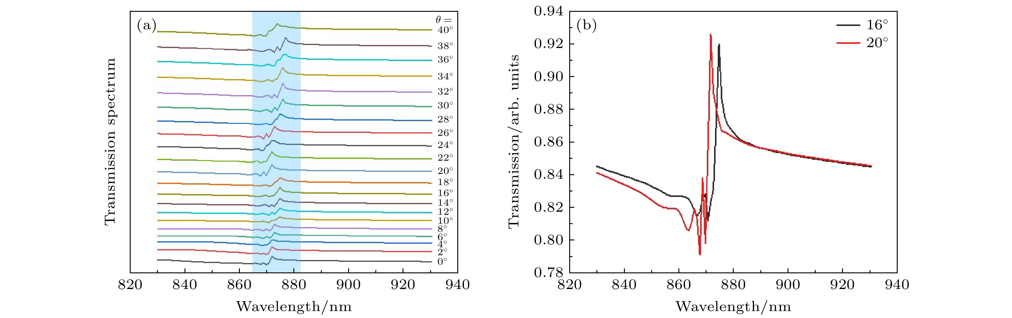
图 5 纳米天线透射光谱和夹角的关系 (a) FDTD仿真计算的纳米天线阵列的透射光谱随θ角的变化图; (b) θ = 16°, 20°时的透射全谱
Fig. 5. Transmission spectra with the different θ: (a) Transmission spectra of the nano-antenna array with θ; (b) the typical transmission spectra of θ = 16° and 20° simulated by FDTD method.

图 6 透射尖峰波长处探测器表面电场和坡印亭矢量分布图, 其中夹角θ分别为(a), (b) 0°; (c), (d) 20°; (e), (f) 40°
Fig. 6. Electric field and Poynting vector distribution at the transmission peak wavelength, θ equals to (a), (b) 0°, (c), (d) 20°, (e), (f) 40°.
-
[1] Ijaz S, Rana A S, Ahmad Z, Zubair M, Massoud Y, Mehmood M Q 2022 Adv. Devices Instrument. 2022 9861078
Google Scholar
[2] Zhang L, Cui T J 2021 Research 2021 9802673
Google Scholar
[3] Xing H, Fan J, Lu D, Gao Z, Shum P P, Cong L 2022 Adv. Devices Instrument. 2022 9852503
Google Scholar
[4] Fang M, Tan X, Liu Z, Hu B, Wang X 2021 Research 2021 9794329
Google Scholar
[5] Maier S A 2007 Plasmonics: Fundamentals and Applications (Berlin, Heideberg: Springer) pp5–19
[6] Mirin N A, Bao K, Nordlander P 2009 J. Phys. Chem. A 113 4028
Google Scholar
[7] Gallinet B, Martin O J F 2011 ACS Nano 5 8999
Google Scholar
[8] Luk'yanchuk B, Zheludev N I, Maier S A, Halas N J, Nordlander P, Giessen H, Chong C T, 2010 Nat. Mater. 9 707
Google Scholar
[9] Hsu C W, Zhen B, Stone A D, Joannopoulos J D, Soljačić M 2016 Nat. Rev. Mater. 1 16048
Google Scholar
[10] Liang Y, Koshelev K, Zhang F, Lin H, Lin S, Wu J, Jia B, Kivshar Y 2020 Nano Lett. 20 635
Google Scholar
[11] 闫梦, 孙珂, 宁廷银, 赵丽娜, 任莹莹, 霍燕燕 2023 物理学报 72 044202
Google Scholar
Yan M, Sun K, Ning T Y, Zhao L N, Ren Y Y, Huo Y Y 2023 Acta Phys. Sin. 72 044202
Google Scholar
[12] Wu N X, Ma H B, Chen H S, Qian H L 2021 Prog. Electromagn. Res. 172 23
Google Scholar
[13] Liu L L, Zhuo L 2022 Prog. Electromagn. Res. 173 93
Google Scholar
[14] Rogers C, Piggott A Y, Thomson D J, Wiser R F, Opris I E, Fortune S A , Compston A J, Gondarenko A, Meng F, Che X, Reed G T, Nicolaescu R 2021 Nature 590 256
Google Scholar
[15] Fossum E R 1997 IEEE T. Electron Dev. 44 1689
Google Scholar
[16] 李龙珍, 姚旭日, 刘雪峰, 俞文凯, 翟光杰 2014 物理学报 63 224201
Google Scholar
Li L Z, Yao X R, Liu X F, Yu W K, Zhai G J 2014 Acta Phys. Sin. 63 224201
Google Scholar
[17] 吴国安, 罗林保 2018 物理 47 137
Google Scholar
Wu G A, Luo L B 2018 Physics 47 137
Google Scholar
[18] 陈浩, 张晓霞, 王鸿, 姬月华 2018 物理学报 67 118101
Google Scholar
Chen H, Zhang X X, Wang H, Ji Y H 2018 Acta Phys. Sin. 67 118101
Google Scholar
[19] 龙弯, 许中杰 2015 激光与光电子学进展 52 26
Google Scholar
Long W, Xu Z J 2015 Laser Optoelectron. Prog. 52 26
Google Scholar
[20] Nordlander P, Oubre C, Prodan E, Li K, Stockman M I 2004 Nano Lett. 4 899
Google Scholar
[21] Wang H, Brandl D W, Nordlander P, Halas N J 2007 Accounts Chem. Res. 40 53
Google Scholar
[22] Tang B, Jia Z, Huang L, Su J, Jiang C 2021 IEEE J. Sel. Top. Quant. 27 1
Google Scholar
[23] Li L F, Wang J Z, Kang L, Liu W, Yu L, Zheng B J, Brongersma M L, Werner D H, Lan S F, Shi Y, Xu Y, Wang X M 2020 ACS Nano 14 16634
Google Scholar
[24] Goykhman I, Sassi U, Desiatov B, Mazurski N, Milana S, Fazio D, Eiden A, Khurgin J, Shappir J, Levy U, Ferrari A C 2016 Nano Lett. 16 3005
Google Scholar
[25] Wang X, Cheng Z, Xu K, Tsang H K, Xu J B 2013 Nat. Photonics 7 888
Google Scholar
[26] Xu S, Sayanskiy A, Kupriianov, Tuz V R, Kapitanova P, Sun H B, Han W, Kivshar Y S 2019 Adv. Opt. Mater. 7 1801166
Google Scholar
[27] Zhang G, Lan C, Gao R, Wen Y, Zhou J 2019 Adv. Theory Simulat. 2 1900123
Google Scholar
[28] Russell K J, Hu E L 2010 Appl. Phys. Lett. 97 163115
Google Scholar
[29] Wu Z Q, Yang J L, Manjunath N K, Zhang Y J, Feng S R, Lu Y H, Wu J H, Zhao W W, Qiu C Y, Li J F, Lin S S 2018 Adv. Mater. 30 1706527
Google Scholar

 下载:
下载:

计量
- 文章访问数: 791
- PDF下载量: 57
- 被引次数: 0
