


-
GeS2单层已成功制备, 为了进一步扩展其应用范围以及发现新的物理特性, 我们构建扶手椅型GeS2纳米带 (AGeS2NR) 模型, 并采用不同浓度的H或O原子进行边缘修饰, 且对其结构稳定性、电子特性、载流子迁移率以及物理场调控效应进行深入研究. 研究表明边修饰纳米带具有良好的能量与热稳定性. 裸边纳米带是无磁半导体, 而边修饰能改变AGeS2NR的带隙, 使其成为宽带隙或窄带隙半导体, 或金属, 这与边缘态消除或部分消除或产生杂化能带有关, 所以边缘修饰调控扩展了纳米带在电子器件及光学器件领域的应用范围. 此外, 计算发现载流子迁移率对边缘修饰十分敏感, 可以调节纳米带载流子迁移率 (电子、空穴) 的差异达到1个数量级, 同时产生载流子极化达到1个数量级. 研究还表明半导体性纳米带在较大的应变范围内具有保持电子相不变的鲁棒性, 对于保持相关器件电子输运的稳定性是有益的. 绝大部分半导体性纳米带在较高的外电场作用下, 都具有保持半导体特性不变的稳定性, 但带隙随电场增大而明显变小. 总之, 本研究为理解GeS2纳米带特性并研发相关器件提供了理论分析及参考.GeS2 monolayers have been successfully prepared in this work. To further expand their applications and discover new physical properties, we construct armchair-type GeS2 nanoribbons (AGeS2NR) and use different concentrations of H and O atoms for the edge modificationand their structural stabilities, electronic properties, carrier mobilities, and physical field modulation effects are studied in depth. The results show that the edge-modified nanoribbon has a higher energy and thermal stability. The bare edge nanoribbon is a nonmagnetic semiconductor, while the edge modification can change the bandgap of AGeS2NR and make it a wide or narrowed bandgap semiconductor, or a metal, which is closely related to the elimination or partial elimination of the edge states or the creation of hybridization bands. Thus edge modification extends the application range of nanoribbons in the fields of electronic devices and optical devices. In addition, the carrier mobility is found to be very sensitive to the edge modification: the carriers’ (electrons’ and holes’) mobilities of nanoribbons can be adjusted to a difference of up to one order of magnitude, and the difference in carrier mobility polarization can be tuned to one order of magnitude. Strain effect studies reveal that the semiconducting nanoribbons are robust in keeping the electronic phase unchanged over a wide strain range, which is useful for maintaining the stability of the electron transport in the related device. Most of the semiconducting nanoribbons have the stability to keep the semiconducting properties unchanged under high external electric field, but the bandgap can be reduced significantly with the increase of the electric field. In short, this study provides a theoretical analysis and reference for understanding the property of GeS2 nanoribbons and developing related devices.
-
Keywords:
- GeS2 nanoribbons /
- edge modification /
- electronic properties /
- physical field modulation /
- crrier mobility
[1] Novoselov K S, Geim A K, Morozov S V, Jiang D, Zhang Y, Dubonos S V, Grigorieva I V, Firsov A A 2004 Science 306 666
 Google Scholar
[2] Zhuang J C, Xu X, Feng H F, Li Z, Wang X L, Du Y 2015 Sci. Bull. 60 1551
Google Scholar
[3] Tran V, Soklaski R, Liang Y F, Yang L 2014 Phys. Rev. B 89 817
[4] Zhang S L, Guo S Y, Chen Z F, Wang Y L, Gao H J, Gomez-Herrero J, Ares P, Zamora F, Zhu Z, Zeng H B 2018 Chem. Soc. Rev. 47 982
Google Scholar
[5] Song L, Ci L J, Lu H, Sorokin P B, Jin C H, Ni J, Kvashnin A G, Kvashnin D G, Lou J, Yakobson B I, Ajayan P M 2010 Nano Lett. 10 3209
Google Scholar
[6] Qu H Z, Guo S Y, Zhou W H, Wu Z H, Cao J, Li Z, Zeng H B, Zhang S L 2022 Phys. Rev. B 105 075413
Google Scholar
[7] Zhang S L, Zhou W H, Ma Y D, Ji J P, Cai B, Yang S A, Zhu Z, Chen Z F, Zeng H B 2017 Nano Lett. 17 3434
Google Scholar
[8] Li H, Wu J, Yin Z Y, Zhang H 2014 Acc Chem. Res. 47 1067
Google Scholar
[9] Radisavljevic B, Kis A 2013 Nat. Mater. 12 815
Google Scholar
[10] Qi Y, Naumov P G, Ali M N, Rajamathi C R, Schnelle W, Barkalov O, Hanfland M, Wu S, Shekhar C, Sun Y 2016 Nat. Commun. 7 11038
Google Scholar
[11] Nandi P, Rawat A, Ahammed R, Jena N, Sarkar A D 2021 Nanoscale 13 5460
Google Scholar
[12] Chen H, Keiser C, Du S, Gao H J, Sutter P, Sutter E 2017 Phys. Chem. Chem. Phys. 19 32473
Google Scholar
[13] Hahn T, Theo 1983 International Tables for Crystallography (Vol. 1) (Dordrecht: Reidel) p182
[14] Wilson E B, Decius J C, Cross P C 1980 Molecular Vibrations: The Theory of Infrared and Raman Vibrational Spectra (Courier Corporation
[15] Gao R L, Yong Y L, Yuan X B, Hu S, Hou Q H, Kuang Y M 2022 ACS Omega 7 46440
Google Scholar
[16] Ruan X Y, Xiong R, Cui Z, Wen C L, Ma J J, Wang B T, Sa B S 2022 Materials 15 4016
Google Scholar
[17] Mao Y L, Zhang G H 2020 Physica B 581 411673
Google Scholar
[18] Do T N, Hieu N N, Poklonski N A, Nguyen C Q, Hien N D 2021 RSC Adv. 3 28381
[19] Wang X L, Feng W, Shen C, Sun Z H, Qi H B, Yang M, Liu Y H, Wu Y C, Wu X Q 2021 Front. Mater. 8 709757
Google Scholar
[20] Son Y W, Cohen M L, Louie S G 2006 Nature 444 347
Google Scholar
[21] Gan Y J, Sun L T, Banhart F 2008 Small 4 587
Google Scholar
[22] Jippo H, Ohfuchi M J 2013 J. Appl. Phys. 113 183715
Google Scholar
[23] Chen H L, Zhang L, Deng X Q, Sun L, Zhang Z H, Fan Z Q 2021 J. Mater. Chem. C 9 12904
Google Scholar
[24] Brandbyge M, Mozos J L, Ordejon P, Taylor J, Stokbro K 2002 Phys. Rev. B 65 165401
Google Scholar
[25] 徐永虎, 邓小清, 孙琳, 范志强, 张振华 2022 物理学报 71 046102
Google Scholar
Xu Y H, Deng X Q, Sun L, Fan Z Q, Zhang Z H 2022 Acta Phys. Sin. 71 046102
Google Scholar
[26] 曹胜果, 韩佳凝, 李占海, 张振华 2023 物理学报 72 117101
Google Scholar
Cao S G, Han J N, Li Z H, Zhang Z H 2023 Acta Phys. Sin. 72 117101
Google Scholar
[27] Li Z H, Han J N, Cao S G, Zhang Z H 2023 Appl. Surf. Sci. 636 157766
Google Scholar
[28] 汤家鑫, 李占海, 邓小清, 张振华 2023 物理学报 72 167101
Google Scholar
Tang J X, Li Z H, Deng X Q, Zhang Z H 2023 Acta Phys. Sin. 72 167101
Google Scholar
[29] Li Z H, Han J N, Cao S G, Zhang Z H 2023 Appl. Surf. Sci. 614 156095
Google Scholar
[30] Li Z H, Han J N, Cao S G, Zhang Z H 2023 Phys. Rev. B 108 184413
Google Scholar
[31] Perdew J P, Burke K, Ernzerhof M 1996 Phys. Rev. Lett. 77 3865
Google Scholar
[32] Troullier N, Martins J L 1991 Phys. Rev. B 43 1993
Google Scholar
[33] Soler J M, Artacho E, Gale J D, Junquera J, Garcia A 2002 J. Phys. Condens. Matter 14 2745
Google Scholar
[34] Biswas R, Hamann D R 1986 Phys. Rev. B 34 895
Google Scholar
[35] Bardeen J, Shockley W 1950 Phys. Rev. 80 72
Google Scholar
[36] Yuan P F, Fan Z Q, Zhang Z H 2017 Carbon 124 228
Google Scholar
[37] Long M Q, Tang L, Wang D, Li Y L, Shuai Z G 2011 ACS Nano 5 2593
Google Scholar
[38] Beleznay F B, Bogár F, Ladik J, 2003 J. Chem. Phys. 119 5690
Google Scholar
[39] Han J N, He X, Fan Z Q, Zhang Z H 2019 Phys. Chem. Chem. Phys. 21 1830
Google Scholar
[40] Zhao T, Fan Z Q, Zhang Z H, Zhou R L 2019 J. Phys. D Appl. Phys. 52 475301
Google Scholar
[41] Zhang Z H, Liu X F, Yu J, Hang Y, Li Y, Guo Y F, Xu Y, Sun X, Zhou J X, Guo W L 2016 Wires Comput. Mol. Sci. 6 324
Google Scholar
[42] Desai S B, Seol G, Kang J S, Fang H, Battaglia C, Kapadia R 2014 Nano Lett. 14 4592
Google Scholar
-
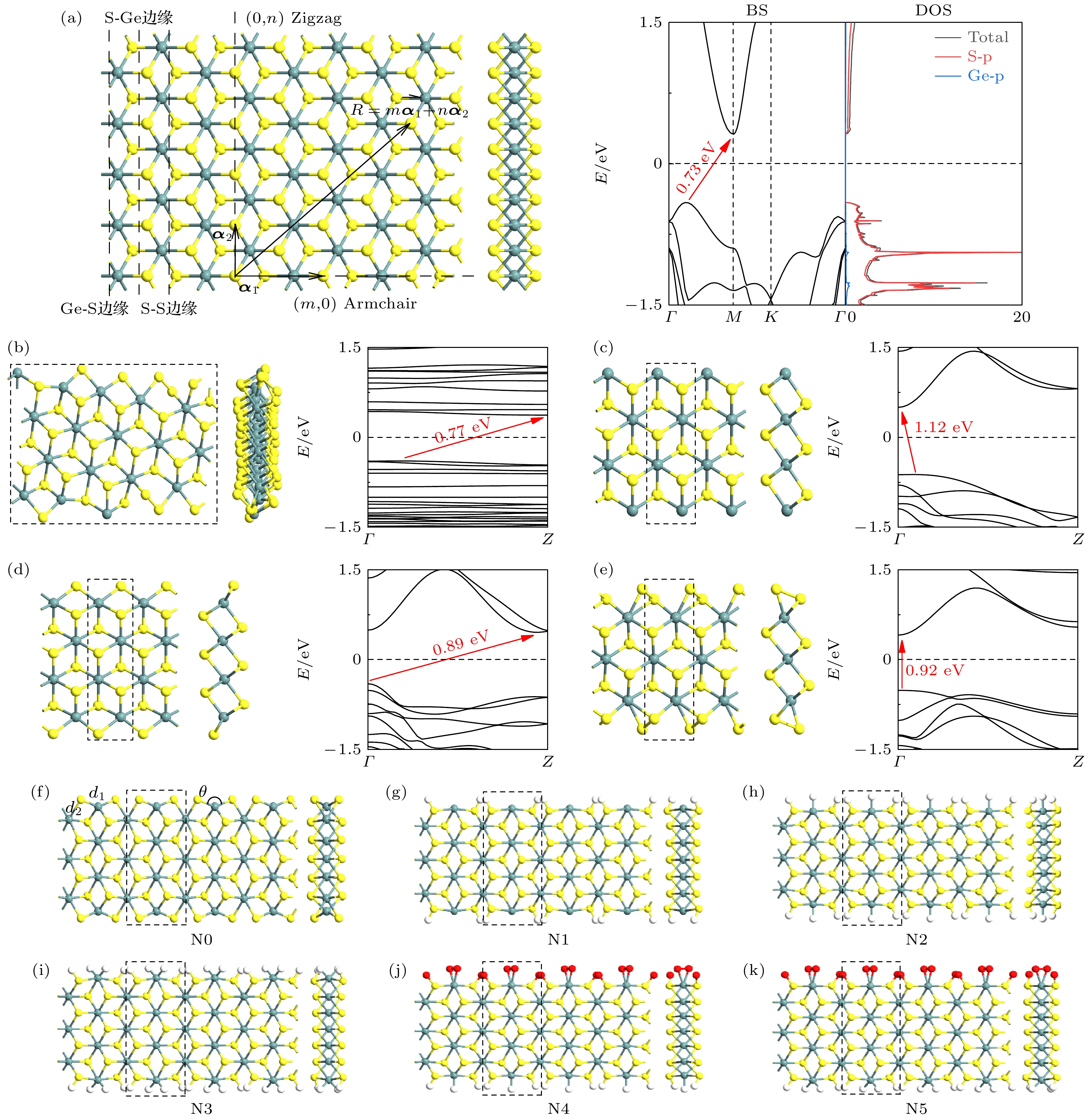
图 1 (a) 2D GeS2原子结构及其能带结构和轨道投影态密度. 优化之后裸边及锯齿型纳米带的几何结构及能带结构 (b) 手性纳米带; (c) Ge-S边缘锯齿型纳米带; (d) S-Ge边缘锯齿型纳米带; (e) S-S边缘锯齿型纳米带. 优化之后扶手椅型纳米带的几何结构 (f) 裸边NR (N0); (g) H-S-NR (N1); (h) H-NR-H (N2); (i) H2H-NR-H2H (N3); (j) H-NR-O2O (N4), (k) H2H-NR-O2O (N5)
Fig. 1. (a) 2D GeS2 atomic structure and its band structure and orbital projection density. Optimized geometries and its band structure: (b) Chiral nanoribbon; (c) Ge-S edge ZGeS2NR; (d) S-Ge edge ZGeS2NR; (e) S-S edge ZGeS2NR. Optimized geometries: (f) Bare-edged NR (N0); (g) H-S-NR (N1); (h) H-NR-H (N2); (i) H2H-NR-H2H (N3); (j) H-NR-O2O (N4); (k) H2H-NR-O2O (N5).
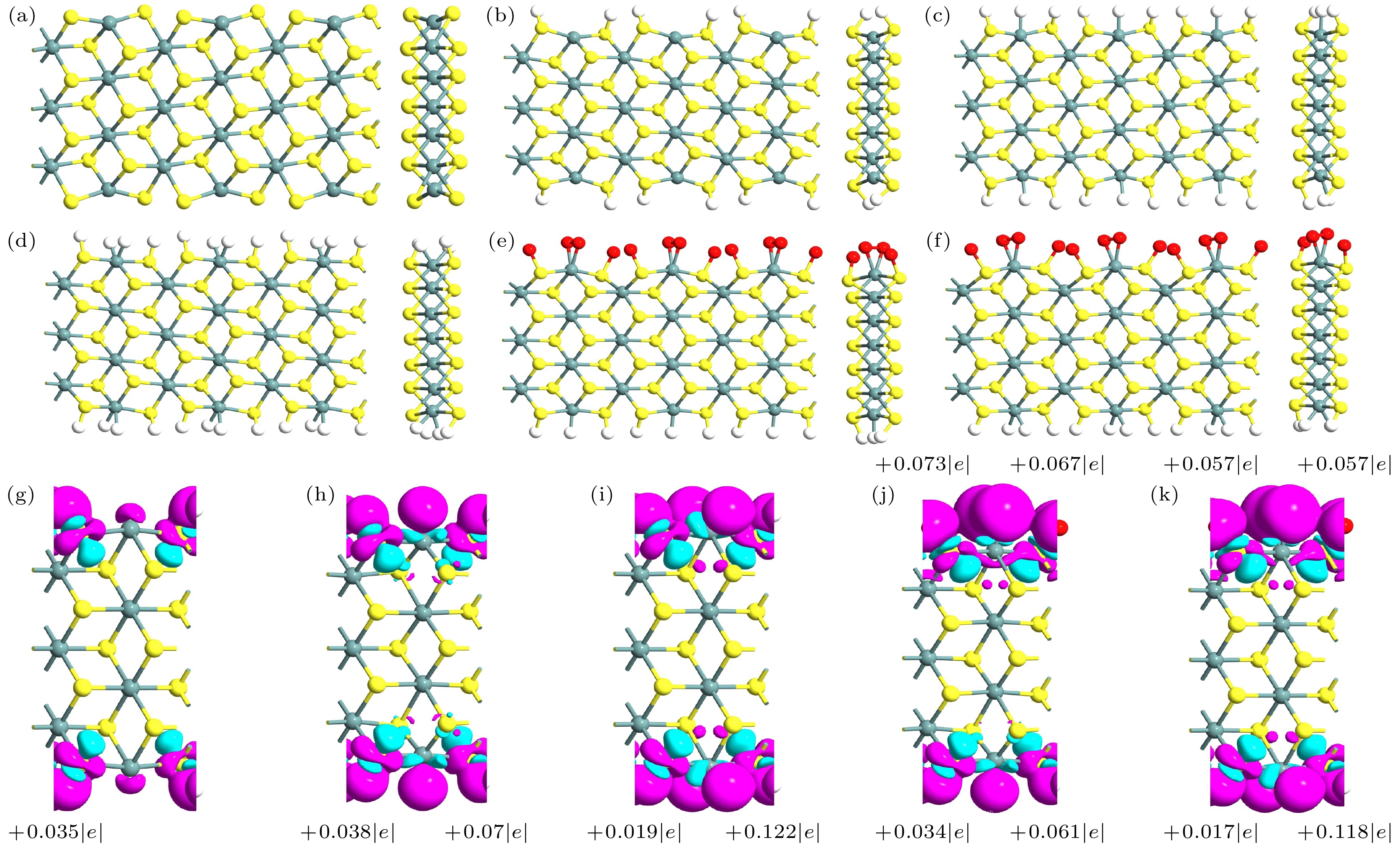
图 2 淬火后纳米带的几何结构 (a) N0, (b) N1, (c) N2, (d) N3, (e) N4, (f) N5; 纳米带的电荷密度差 (g) N1, (h) N2, (i) N3, (j) N4, (k) N5; 青色表示失去电子, 洋红色表示得到电子, 等值面为 0.005 e/Å3, 每个图旁边的数字表示H或O获得的电子数量
Fig. 2. Geometry of quenched nanoribbons: (a) N0, (b) N1, (c) N2, (d) N3, (e) N4, (f) N5. Differential charge densities of nanoribbons: (g) N1, (h) N2, (i) N3, (j) N4, (k) N5. Cyan denotes loss of electrons, magenta denotes gain of electrons, and the isosurfaces are 0.005 e/Å3. Numbers next to each plot denote the number of electrons gained by either H or O.

图 3 纳米带的能带结构、投影态密度及部分电荷密度 (a) N0, (b) N1, (c) N2, (d) N3, (e) N4, (f) N5, 等值面为 0.02|e|Å–3
Fig. 3. The band structure, projected density of states and partial charge density for nanoribbons: (a) N0, (b) N1, (c) N2, (d) N3, (e) N4, (f) N5, where equivalent surface is set to 0.02|e| Å–3.

图 4 半导体性纳米带Ni (i = 0, 1, 3, 5)沿输运方向的电子和空穴的(a) 有效质量m*, (b) 形变势常数E1和拉伸模量C, (c) 载流子迁移率µ (其中h对应空穴, e对应电子); (d) N1纳米带的CBM和VBM的Bloch态, 等值面为0.05e/Å3
Fig. 4. (a) Effective mass m*, (b) deformation potential constant E1 and tensile modulus C, (c) carrier mobility μ for electrons and holes in semiconducting nanoribbons Ni (i = 0, 1, 3, 5) along the transport direction, where h for holes and e for electrons; (d) Bloch states of CBM and VBM for N1 nanoribbon, and the isosurfaces are 0.05e/Å3.
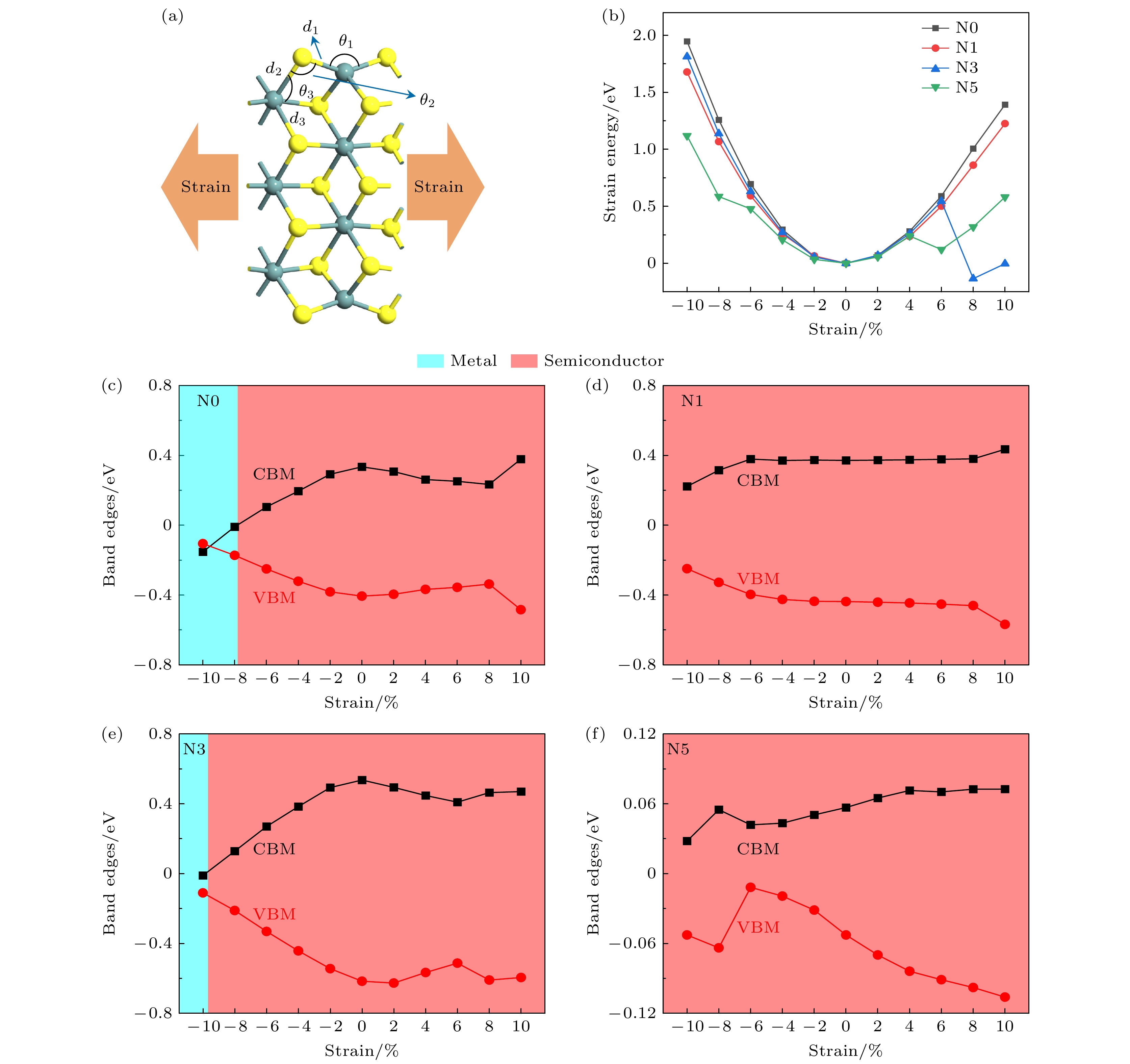
图 5 (a) 施加应变示意图; (b) 半导体性纳米带Ni (i = 0, 1, 3, 5) 的应变能与应变的关系. Ni的带边(CBM和VBM) 和电子相随应变ε的演变 (c) N0; (d) N1; (e) N3; (f) N5
Fig. 5. (a) Schematic diagram of applied strain; (b) strain energy versus strain for semiconducting nanoribbons Ni (i = 0, 1, 3, 5). Evolution of band edges (CBM and VBM) and electronic phase versus strain ε: (c) N0; (d) N1; (e) N3; (f) N5.
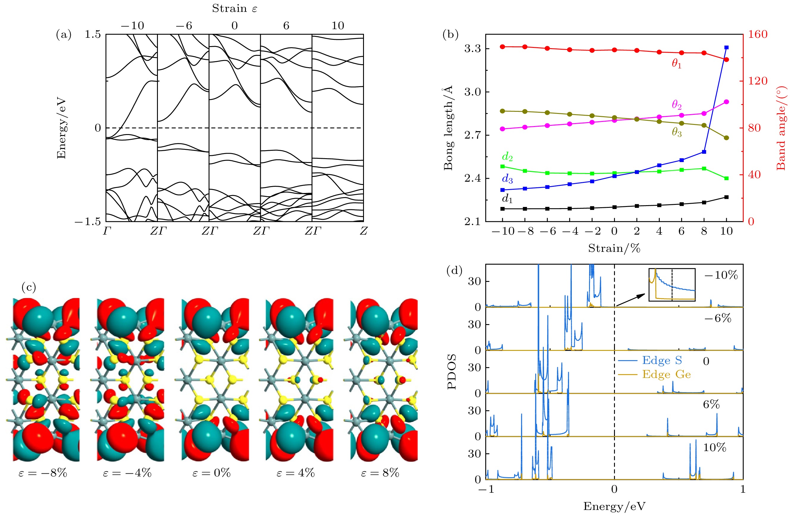
图 6 N0的应变效应 (a) 能带结构与应变的关系; (b) 键长与键角随应变的变化; (c) 5种典型应变HVB在Z点的布洛赫态, 等值面为 0.04e/Å3; (d) 5种典型应变下边缘上S原子和Ge原子的投影态密度 (PDOS)
Fig. 6. Strain effects for N0: (a) Band structure versus strain; (b) bond length and bond angle versus strain; (c) Bloch states at the Z point for five typical strains of HVB, with an isosurface of 0.04e/Å3; (d) projected densities of states (PDOS) for S and Ge atoms on the edge at five typical strains.
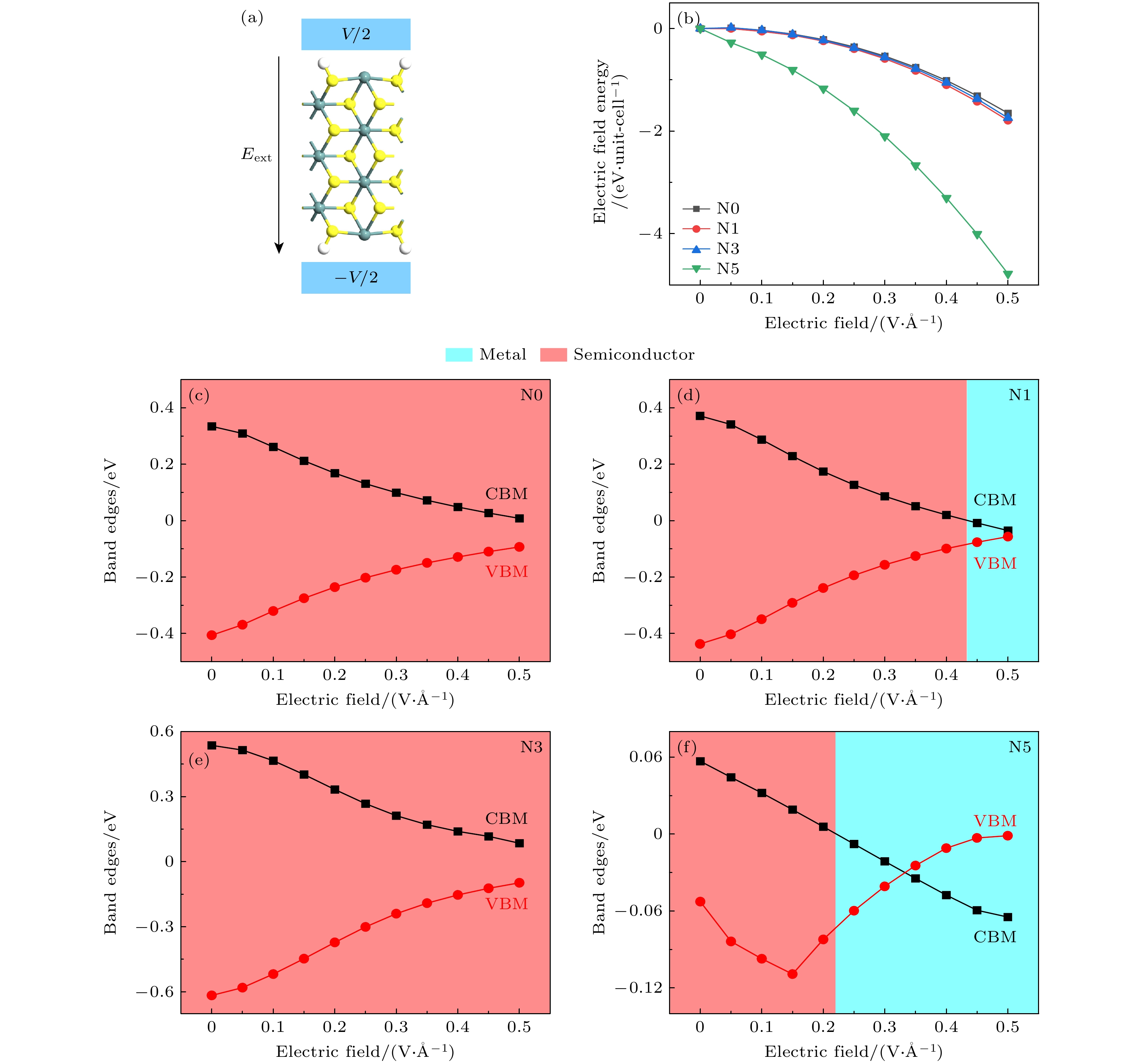
图 7 (a) 施加电场示意图; (b) 半导体性纳米带Ni (i = 0, 1, 3, 5) 的电场能与电场的关系. Ni的带边 (CBM和VBM) 和电子相随电场的演变 (c) N0; (d) N1; (e) N3; (f) N5
Fig. 7. (a) Schematic diagram of applied external electric field; (b) electric field energy versus electric field for the semiconducting nanoribbons Ni (i = 0, 1, 3, 5). Evolution of band edges (CBM and VBM) and electronic phases of Ni with electric field: (c) N0; (d) N1; (e) N3; (f) N5.
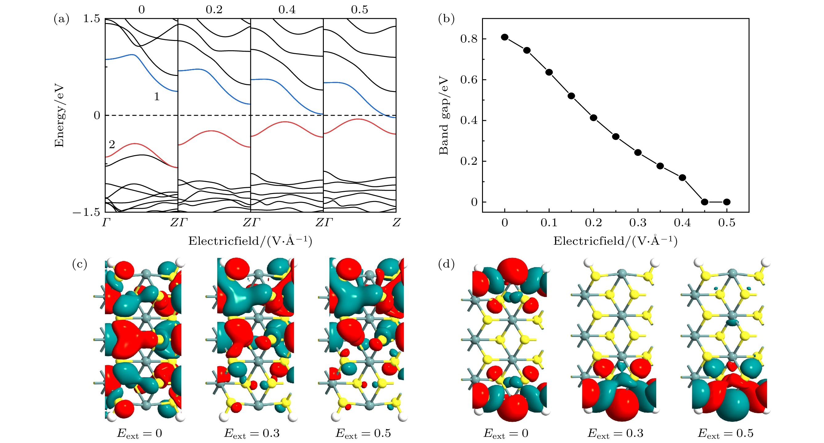
图 8 N1的电场效应 (a) 能带结构与电场的关系; (b)带隙随电场的变化; (c) 3个典型电场值下, 子带1在Z点的布洛赫态; (d) 3个典型电场值下, 子带2在Z点的布洛赫态, 等值面设为 0.06e/Å3
Fig. 8. Electric field effects for N1: (a) Band structure versus electric field; (b) band gap versus electric field; (c) Bloch state of subband 1 at the Z point for three typical values of the electric field; (d) Bloch state of subband 2 at the Z point for three typical values of the electric field, with an isosurface of 0.06e/Å3.
表 1 纳米带Ni (i = 0, 1, 2, 3, 4, 5)的边形成能Ef (单位: eV/Å)和带边缘的几何参数, 即S—Ge键长d1和d2 (单位: Å)以及两个边缘S—Ge键之间的夹度θ (单位: (°))
Table 1. Edge formation energy Ef (in eV/Å) and geometrical parameters of the ribbon edges for the nanoribbon Ni (i = 0, 1, 2, 3, 4, 5), i.e., S—Ge bond lengths d1 and d2 (in Å) and bond angle θ (in (°)) between the two edge S—Ge bonds.
Structure N0 N1 N2 N3 N4 N5 d1 /Å 2.44 2.42 2.51 2.49 2.49 2.52 d2 /Å 2.20 2.69 2.53 2.50 2.43 2.40 θ/(°) 146.64 170.49 175.89 166.77 176.11 179.07 Ef /(eV·Å–1) 0 –1.293 –1.735 –2.323 –2.704 –2.996  下载: 导出CSV
-
[1] Novoselov K S, Geim A K, Morozov S V, Jiang D, Zhang Y, Dubonos S V, Grigorieva I V, Firsov A A 2004 Science 306 666
Google Scholar
[2] Zhuang J C, Xu X, Feng H F, Li Z, Wang X L, Du Y 2015 Sci. Bull. 60 1551
Google Scholar
[3] Tran V, Soklaski R, Liang Y F, Yang L 2014 Phys. Rev. B 89 817
[4] Zhang S L, Guo S Y, Chen Z F, Wang Y L, Gao H J, Gomez-Herrero J, Ares P, Zamora F, Zhu Z, Zeng H B 2018 Chem. Soc. Rev. 47 982
Google Scholar
[5] Song L, Ci L J, Lu H, Sorokin P B, Jin C H, Ni J, Kvashnin A G, Kvashnin D G, Lou J, Yakobson B I, Ajayan P M 2010 Nano Lett. 10 3209
Google Scholar
[6] Qu H Z, Guo S Y, Zhou W H, Wu Z H, Cao J, Li Z, Zeng H B, Zhang S L 2022 Phys. Rev. B 105 075413
Google Scholar
[7] Zhang S L, Zhou W H, Ma Y D, Ji J P, Cai B, Yang S A, Zhu Z, Chen Z F, Zeng H B 2017 Nano Lett. 17 3434
Google Scholar
[8] Li H, Wu J, Yin Z Y, Zhang H 2014 Acc Chem. Res. 47 1067
Google Scholar
[9] Radisavljevic B, Kis A 2013 Nat. Mater. 12 815
Google Scholar
[10] Qi Y, Naumov P G, Ali M N, Rajamathi C R, Schnelle W, Barkalov O, Hanfland M, Wu S, Shekhar C, Sun Y 2016 Nat. Commun. 7 11038
Google Scholar
[11] Nandi P, Rawat A, Ahammed R, Jena N, Sarkar A D 2021 Nanoscale 13 5460
Google Scholar
[12] Chen H, Keiser C, Du S, Gao H J, Sutter P, Sutter E 2017 Phys. Chem. Chem. Phys. 19 32473
Google Scholar
[13] Hahn T, Theo 1983 International Tables for Crystallography (Vol. 1) (Dordrecht: Reidel) p182
[14] Wilson E B, Decius J C, Cross P C 1980 Molecular Vibrations: The Theory of Infrared and Raman Vibrational Spectra (Courier Corporation
[15] Gao R L, Yong Y L, Yuan X B, Hu S, Hou Q H, Kuang Y M 2022 ACS Omega 7 46440
Google Scholar
[16] Ruan X Y, Xiong R, Cui Z, Wen C L, Ma J J, Wang B T, Sa B S 2022 Materials 15 4016
Google Scholar
[17] Mao Y L, Zhang G H 2020 Physica B 581 411673
Google Scholar
[18] Do T N, Hieu N N, Poklonski N A, Nguyen C Q, Hien N D 2021 RSC Adv. 3 28381
[19] Wang X L, Feng W, Shen C, Sun Z H, Qi H B, Yang M, Liu Y H, Wu Y C, Wu X Q 2021 Front. Mater. 8 709757
Google Scholar
[20] Son Y W, Cohen M L, Louie S G 2006 Nature 444 347
Google Scholar
[21] Gan Y J, Sun L T, Banhart F 2008 Small 4 587
Google Scholar
[22] Jippo H, Ohfuchi M J 2013 J. Appl. Phys. 113 183715
Google Scholar
[23] Chen H L, Zhang L, Deng X Q, Sun L, Zhang Z H, Fan Z Q 2021 J. Mater. Chem. C 9 12904
Google Scholar
[24] Brandbyge M, Mozos J L, Ordejon P, Taylor J, Stokbro K 2002 Phys. Rev. B 65 165401
Google Scholar
[25] 徐永虎, 邓小清, 孙琳, 范志强, 张振华 2022 物理学报 71 046102
Google Scholar
Xu Y H, Deng X Q, Sun L, Fan Z Q, Zhang Z H 2022 Acta Phys. Sin. 71 046102
Google Scholar
[26] 曹胜果, 韩佳凝, 李占海, 张振华 2023 物理学报 72 117101
Google Scholar
Cao S G, Han J N, Li Z H, Zhang Z H 2023 Acta Phys. Sin. 72 117101
Google Scholar
[27] Li Z H, Han J N, Cao S G, Zhang Z H 2023 Appl. Surf. Sci. 636 157766
Google Scholar
[28] 汤家鑫, 李占海, 邓小清, 张振华 2023 物理学报 72 167101
Google Scholar
Tang J X, Li Z H, Deng X Q, Zhang Z H 2023 Acta Phys. Sin. 72 167101
Google Scholar
[29] Li Z H, Han J N, Cao S G, Zhang Z H 2023 Appl. Surf. Sci. 614 156095
Google Scholar
[30] Li Z H, Han J N, Cao S G, Zhang Z H 2023 Phys. Rev. B 108 184413
Google Scholar
[31] Perdew J P, Burke K, Ernzerhof M 1996 Phys. Rev. Lett. 77 3865
Google Scholar
[32] Troullier N, Martins J L 1991 Phys. Rev. B 43 1993
Google Scholar
[33] Soler J M, Artacho E, Gale J D, Junquera J, Garcia A 2002 J. Phys. Condens. Matter 14 2745
Google Scholar
[34] Biswas R, Hamann D R 1986 Phys. Rev. B 34 895
Google Scholar
[35] Bardeen J, Shockley W 1950 Phys. Rev. 80 72
Google Scholar
[36] Yuan P F, Fan Z Q, Zhang Z H 2017 Carbon 124 228
Google Scholar
[37] Long M Q, Tang L, Wang D, Li Y L, Shuai Z G 2011 ACS Nano 5 2593
Google Scholar
[38] Beleznay F B, Bogár F, Ladik J, 2003 J. Chem. Phys. 119 5690
Google Scholar
[39] Han J N, He X, Fan Z Q, Zhang Z H 2019 Phys. Chem. Chem. Phys. 21 1830
Google Scholar
[40] Zhao T, Fan Z Q, Zhang Z H, Zhou R L 2019 J. Phys. D Appl. Phys. 52 475301
Google Scholar
[41] Zhang Z H, Liu X F, Yu J, Hang Y, Li Y, Guo Y F, Xu Y, Sun X, Zhou J X, Guo W L 2016 Wires Comput. Mol. Sci. 6 324
Google Scholar
[42] Desai S B, Seol G, Kang J S, Fang H, Battaglia C, Kapadia R 2014 Nano Lett. 14 4592
Google Scholar

 下载:
下载:
计量
- 文章访问数: 775
- PDF下载量: 35
- 被引次数: 0
