


-
GaAs-based semiconductor doping technology, in which impurity energy levels are introduced into the band gap, can give rise to a decisive effect on its electrical and optical properties. When GaAs material is reduced to one-dimensional nanoscale, due to the increase of specific surface area, wurtzite- zinc blende coexisting structure is prone to appearing. GaAs nanowire doping can not only adjust its electro-optical properties, but also have a significant regulatory effect on its structural phase transition. The effects of beryllium (Be) and silicon (Si) doping on crystal structure and optical properties of gallium arsenide (GaAs) nanowires (NWs) are studied in this paper. Primitive, Si-doped and Be-doped GaAs NWs are grown on Si(111) substrates by molecular beam epitaxy in virtue of the self-catalyzed growth mechanism. The Raman spectra of primitive, Si-doped and Be-doped GaAs NWs are measured. The E2 mode peak unique to the WZ structure of primitive GaAs NWs is found in the Raman spectrum, and the E2 mode peak in the Raman spectrum of Si-doped GaAs NWs weakens or even disappears. Moreover, The E2 mode peak is not found in the Raman spectrum of Be-doped GaAs NWs. Furthermore, the structural changes of GaAs NWs are observed more intuitively by high-resolution transmission electron microscopy (HRTEM) and selected area electron diffraction (SAED). The PL spectra show that the wurtzite (WZ)-zinc blende (ZB) mixed phase II-type luminescence exists in primitive GaAs NWs, then the luminescence disappears due to Si or Be doping and turns into impurity defect related luminescence.
-
Keywords:
- GaAs nanowires /
- structure /
- doping /
- molecular beam epitaxy
[1] Kasai S, Asai T 2008 Appl. Phys. Express 1 083001
 Google Scholar
[2] Saxena D, Mokkapati S, Parkinson P, Jiang N, Gao Q, Tan H H, Jagadish C 2013 Nat. Photonics 7 963
Google Scholar
[3] Zhu X, Lin F, Zhang Z, Chen X, Huang H, Wang D, Tang J, Fang X, Fang D, Ho J C, Liao L, Wei Z 2020 Nano Lett. 20 2654
Google Scholar
[4] Krogstrup P, Jørgensen H I, Heiss M, Demichel O, Holm J V, Aagesen M, Nygard J, Fontcuberta i Morral A 2013 Nat. Photonics 7 306
Google Scholar
[5] Glas F, Harmand J C, Patriarche G 2007 Phys. Rev. Lett. 99 146101
Google Scholar
[6] Parkinson P, Joyce H J, Gao Q, Tan H H, Zhang X, Zou J, Jagadish C, Herz L M, Johnston M B 2009 Nano Lett. 9 3349
Google Scholar
[7] Thelander C, Caroff P, Plissard S, Dey A W, Dick K A 2011 Nano Lett. 11 2424
Google Scholar
[8] Woo R L, Xiao R, Kobayashi Y, Gao L, Goel N, Hudait M K, Mallouk T E, Hicks R F 2008 Nano Lett. 8 4664
Google Scholar
[9] Gil E, Dubrovskii V G, Avit G, André Y, Leroux C, Lekhal K, Grecenkov J, Trassoudaine A, Castelluci D, Monier G, Ramdani R M, Robert-Goumet C, Bideux L, Harmand J C, Glas F 2014 Nano Lett. 14 3938
Google Scholar
[10] Lehmann S, Wallentin J, Jacobsson D, Deppert K, Dick K A 2013 Nano Lett. 13 4099
Google Scholar
[11] Panciera F, Baraissov Z, Patriarche G, Dubrovskii V G, Glas F, Travers L, Mirsaidov U, Harmand J C 2020 Nano Lett. 20 1669
Google Scholar
[12] Jacobsson D, Panciera F, Tersoff J, Reuter M C, Lehmann S, Hofmann S, Dick K A, Ross F M 2016 Nature 531 317
Google Scholar
[13] Dheeraj D L, Patriarche G, Zhou H, Hoang T B, Moses A F, Grønsberg S, van Helvoort A T J, Fimland B O, Weman H 2008 Nano Lett. 8 4459
Google Scholar
[14] Ren D D, Dheeraj D L, Jin C J, Nilsen J S, Huh J, Reinertsen J F, Munshi A M, Gustafsson A, van Helvoort A T J, Weman H, Fimland B O 2016 Nano Lett. 16 1201
Google Scholar
[15] Zhang Y, Sun Z, Sanchez A M, Ramsteiner M, Aagesen M, Wu J, Kim D, Jurczak P, Huo S, Lauhon L J, Liu H Y 2018 Nano Lett. 18 81
Google Scholar
[16] Lu Z, Zhang Z, Chen P, Shi S, Yao L, Zhou C, Zhou X, Zou J, Lu W 2014 Appl. Phys. Lett. 105 162102
Google Scholar
[17] Zhang Y, Fonseka H A, Aagesen M, Gott J A, Sanchez A M, Wu J, Jurczak P, Huo S, Liu H Y 2017 Nano Lett. 17 4946
Google Scholar
[18] Spirkoska D, Arbiol J, Gustafsson A, Conesa-Boj S, Glas F, Zardo I, Heigoldt M, Gass M H, Bleloch A L, Estrade S, Kaniber M, Rossler J, Peiro F, Morante J R, Abstreiter G, Samuelson L, Fontcuberta i Morral A 2009 Phys. Rev. B 80 245325
Google Scholar
[19] Jahn U, Lähnemann J, Pfüller C, Brandt O, Breuer S, Jenichen B, Ramsteiner M, Geelhaar L, Riechert H 2012 Phys. Rev. B 85 045323
Google Scholar
[20] Zardo I, Conesa-Boj S, Peiro F, Morante J R, Arbiol J, Uccelli E, Abstreiter G, Fontcuberta i Morral A 2009 Phys. Rev. B 80 245324
Google Scholar
[21] Ketterer B, Heiss M, Uccelli E, Arbiol J, Fontcuberta i Morral A 2011 ACS Nano 5 7585
Google Scholar
[22] Ketterer B, Uccelli E, Fontcuberta i Morral A 2012 Nanoscale 4 1789
Google Scholar
[23] Goktas N I, Fiordaliso E M, LaPierre R R 2018 Nanotechnology 29 234001
Google Scholar
[24] Chiu Y S, Ya M H, Su W S, Chen Y F 2002 J. Appl. Phys. 92 5810
Google Scholar
[25] 王鹏华, 唐吉龙, 亢玉彬, 方铉, 房丹, 王登魁, 林逢源, 王晓华, 魏志鹏 2019 物理学报 68 087803
Google Scholar
Wang P H, Tang J L, Kang Y B, Fang X, Fang D, Wang D, Lin F Y, Wang X H, Wei Z P 2019 Acta Phys. Sin. 68 087803
Google Scholar
[26] Ge X, Wang D, Gao X, Fang X, Niu S, Gao H, Tang J, Wang X, Wei Z, Chen R 2017 Phys. Status Solidi RRL 11 1700001
Google Scholar
[27] Simmonds P J, Babu Laghumavarapu R, Sun M, Lin A, Reyner C J, Liang B, Huffaker D L 2012 Appl. Phys. Lett. 100 243108
Google Scholar
[28] Arab S, Yao M, Zhou C, Dapkus P D, Cronin S B 2016 Appl. Phys. Lett. 108 182106
Google Scholar
[29] Liu B, Cheng C W, Chen R, Shen Z X, Fan H J, Sun H D 2010 J. Phys. Chem. C 114 3407
Google Scholar
[30] Zhu L D, Chan K T, Wagner D K, Ballantyne J M 1985 J. Appl. Phys. 57 5486
Google Scholar
[31] Neu G, Teisseire M, Freundlich A, Horton C, Ignatiev A 1999 Appl. Phys. Lett. 74 3341
Google Scholar
[32] Dingle R 1969 Phys. Rev. 184 788
Google Scholar
[33] Hudait M K, Clavel M B, Saluru S, Liu J S, Meeker M A, Khodaparast G A, Bodnar R J 2018 AIP Adv. 8 115119
Google Scholar
[34] Scott G B, Duggan G, Dawson P, Weimann G 1981 J. Appl. Phys. 52 6888
Google Scholar
-
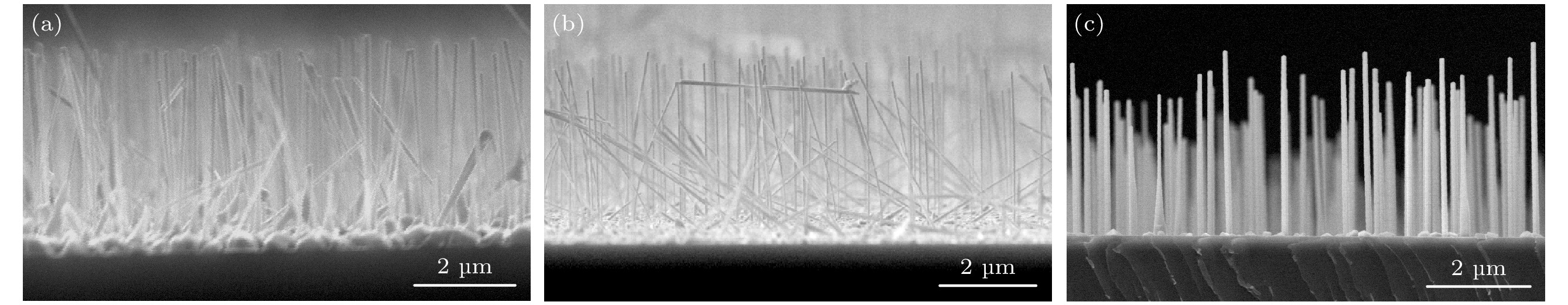
图 1 GaAs纳米线SEM侧视图 (a)本征GaAs纳米线; (b) Si掺杂GaAs纳米线; (c) Be掺杂GaAs纳米线
Figure 1. The side-view SEM images of GaAs NWs: (a) Intrinsic GaAs NWs; (b) Si-doped GaAs NWs; (c) Be-doped GaAs NWs.
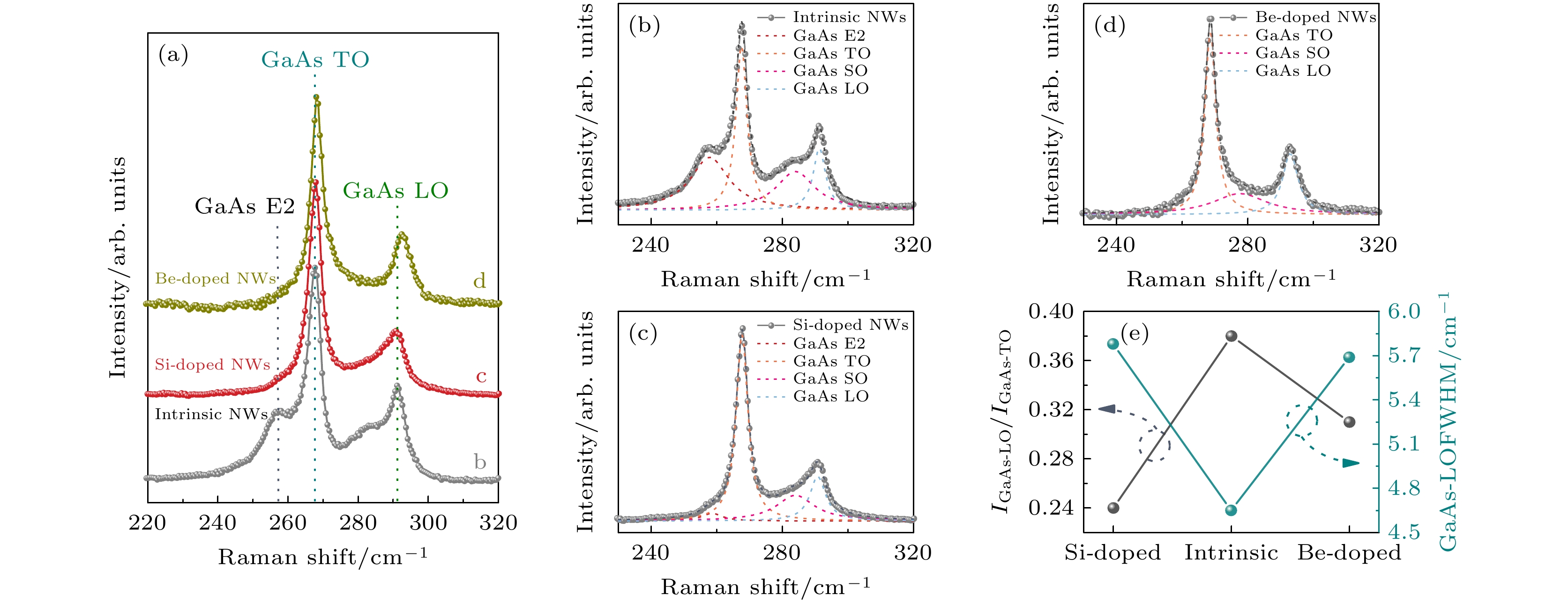
图 2 (a)本征, Si掺杂及Be掺杂GaAs纳米线的Raman光谱; (b)本征, (c) Si掺杂和(d) Be掺杂GaAs纳米线的多洛伦兹拟合图; (e)所有GaAs纳米线的GaAs LO与GaAs TO强度比值及GaAs LO的FWHM图
Figure 2. (a) The Raman spectra of intrinsic, Si-doped and Be-doped GaAs NWs; (b) intrinsic, (c) Si-doped, and (d) Be-doped GaAs NWs are fitted by multi-Lorentzian functions; (e) intensity ratio of ILO/ITO and FWHM of GaAs LO for intrinsic, Si-doped and Be-doped GaAs NWs.
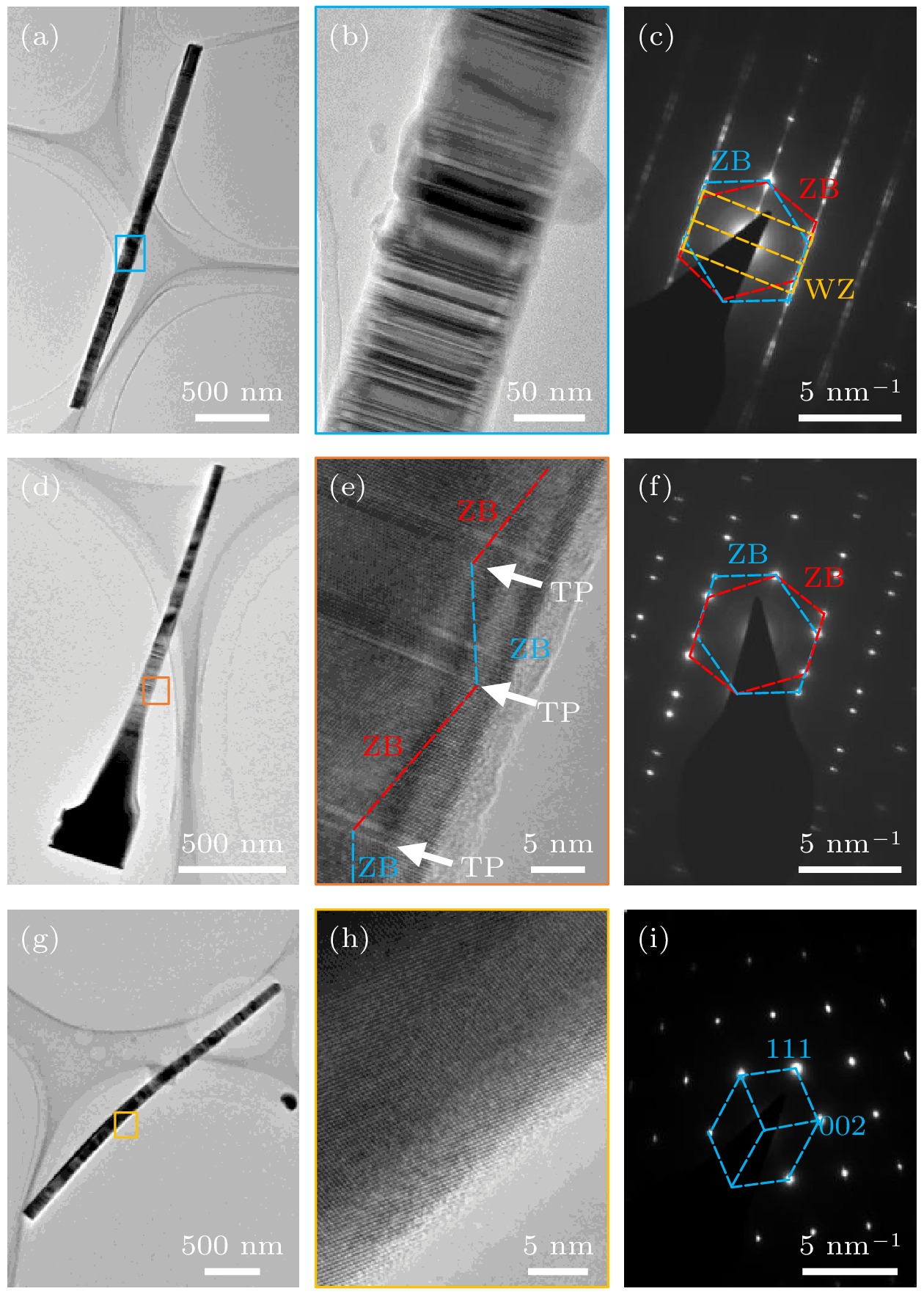
图 3 GaAs纳米线的TEM和选区电子衍射图. 本征GaAs纳米线 (a)低分辨TEM, (b)高分辨TEM及(c)对应的选区电子衍射图样; Si掺杂GaAs纳米线(d)低分辨TEM, (e)高分辨TEM及(f)对应的选区电子衍射图样; Be掺杂GaAs纳米线(g)低分辨TEM, (h)高分辨TEM及(i)对应的选区电子衍射图样
Figure 3. TEM and SAED of GaAs NWs: (a) Low-TEM, (b) HRTEM and (c) SAED of intrinsic GaAs NW; (d) low-TEM, (e) HRTEM and (f) SAED of Si-doped GaAs NW; (g) low-TEM, (h) HRTEM and (i) SAED of Be-doped GaAs NW.
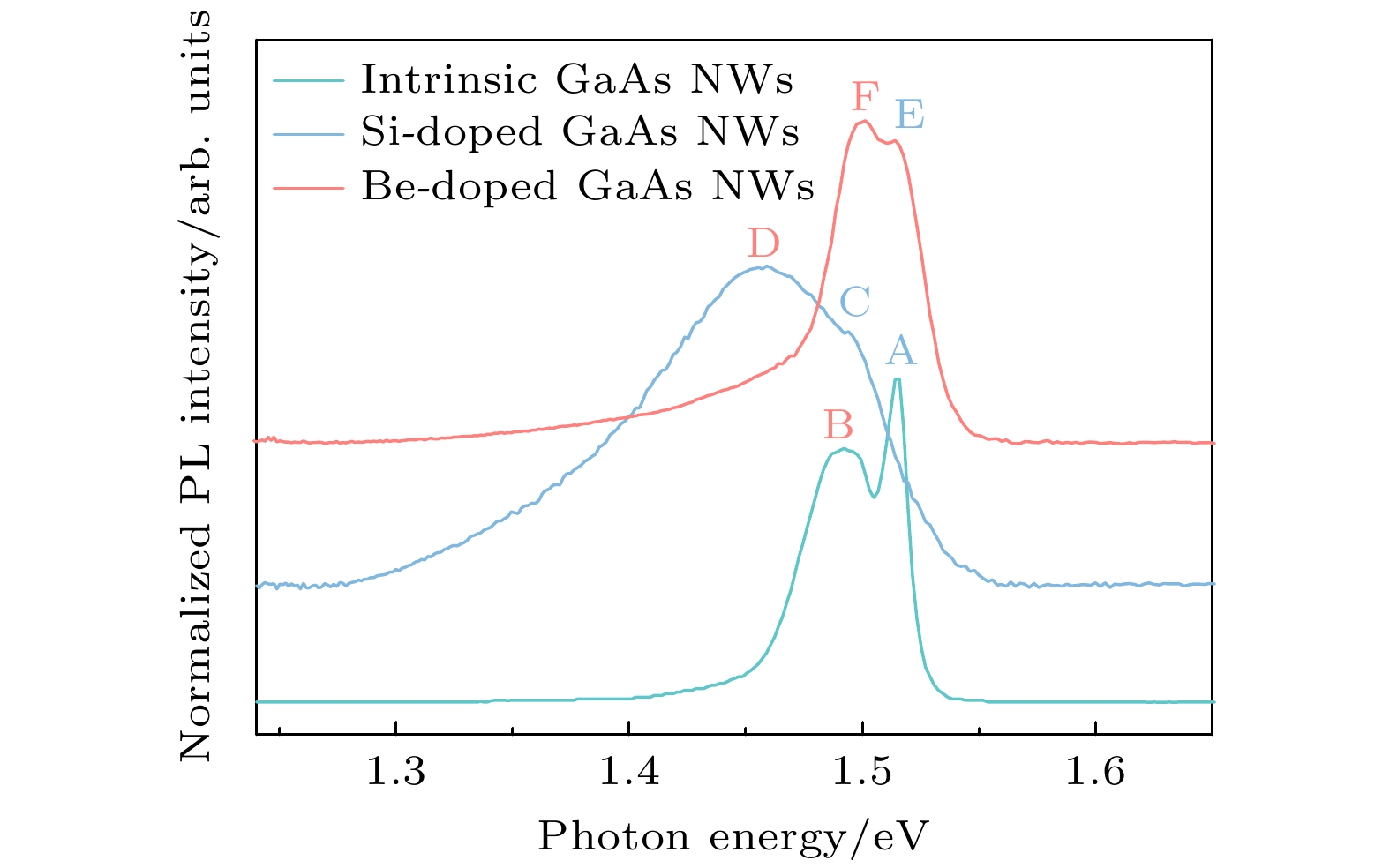
图 4 本征, Si掺杂和Be掺杂GaAs纳米线的低温(at 10 K)下光致发光光谱, 激发光源的功率密度为300 mW/cm2
Figure 4. The PL spectra of intrinsic, Si-doped and Be-doped GaAs NWs at low temperature (10 K). The power density of the excitation light source is 300 mW/cm2.
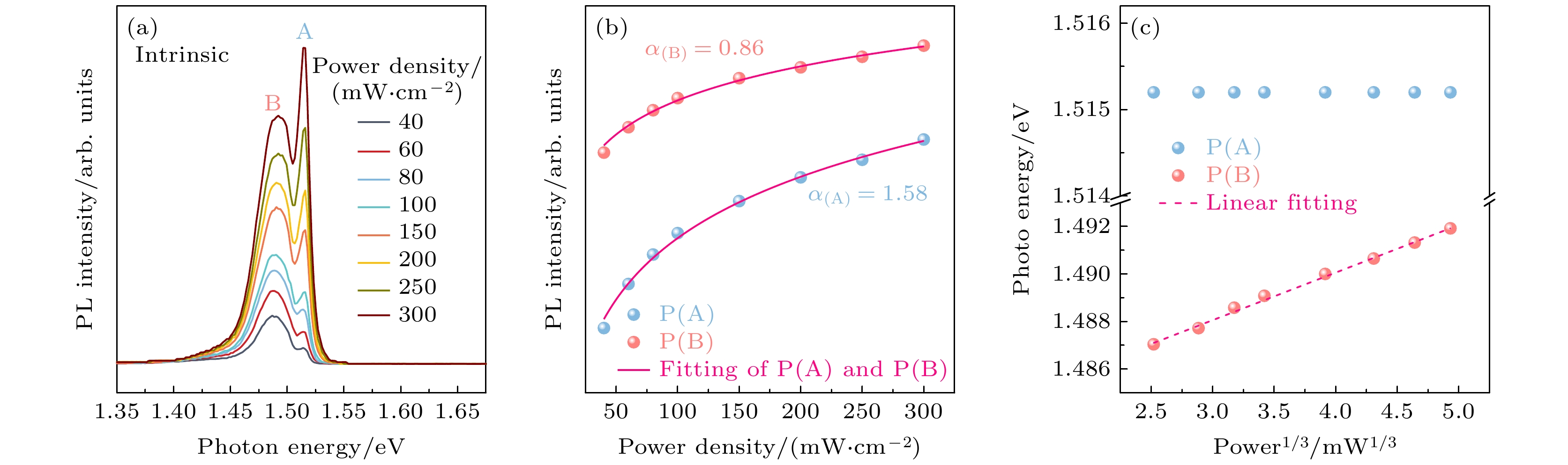
图 5 本征GaAs纳米线光谱图 (a)本征GaAs纳米线在不同功率密度下的PL光谱曲线; (b)本征GaAs纳米线中峰P(A)和峰P(B)强度随功率密度的关系曲线; (c) P(A)和P(B)峰位和功率1/3(P1/3)的关系曲线
Figure 5. The PL spectra of intrinsic GaAs NWs: (a) The PL spectral curves of intrinsic GaAs NWs at different power density; (b) the relationship between peak P (A) and P (B) intensity with power density in intrinsic GaAs NWs; (c) the relationship between P(A) and P(B) peaks and P1/3.
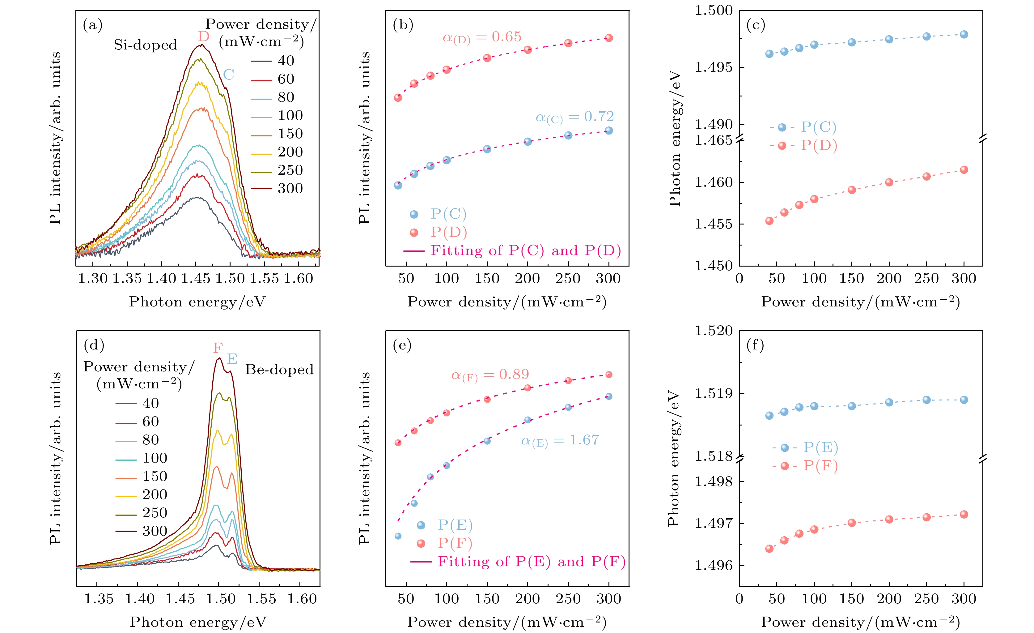
图 6 掺杂GaAs纳米线的光谱图 (a)不同功率密度下Si掺杂GaAs纳米线的PL光谱曲线; Si掺杂GaAs纳米线中P(C)和P(D)积分强度(b)和峰位(c)随功率密度的关系曲线; (d)不同功率密度下Be掺杂GaAs纳米线的PL光谱曲线; Be掺杂GaAs纳米线中P(E)和P(F)峰积分强度(e)和峰位(f)随功率密度的关系曲线
Figure 6. The PL spectra of doped GaAs NWs: (a) The PL spectral curves of Si-doped GaAs NWs at different power density; the relationship between P (C) and P (D) integral intensity (b) and peak positions (c) with power density in Si-doped GaAs NWs; (d) the PL spectral curves of Be-doped GaAs NWs at different power density; The relationship between P (E) and P (F) peak integral intensity (e) and peak positions (f) with power density in Be-doped GaAs NWs.
-
[1] Kasai S, Asai T 2008 Appl. Phys. Express 1 083001
Google Scholar
[2] Saxena D, Mokkapati S, Parkinson P, Jiang N, Gao Q, Tan H H, Jagadish C 2013 Nat. Photonics 7 963
Google Scholar
[3] Zhu X, Lin F, Zhang Z, Chen X, Huang H, Wang D, Tang J, Fang X, Fang D, Ho J C, Liao L, Wei Z 2020 Nano Lett. 20 2654
Google Scholar
[4] Krogstrup P, Jørgensen H I, Heiss M, Demichel O, Holm J V, Aagesen M, Nygard J, Fontcuberta i Morral A 2013 Nat. Photonics 7 306
Google Scholar
[5] Glas F, Harmand J C, Patriarche G 2007 Phys. Rev. Lett. 99 146101
Google Scholar
[6] Parkinson P, Joyce H J, Gao Q, Tan H H, Zhang X, Zou J, Jagadish C, Herz L M, Johnston M B 2009 Nano Lett. 9 3349
Google Scholar
[7] Thelander C, Caroff P, Plissard S, Dey A W, Dick K A 2011 Nano Lett. 11 2424
Google Scholar
[8] Woo R L, Xiao R, Kobayashi Y, Gao L, Goel N, Hudait M K, Mallouk T E, Hicks R F 2008 Nano Lett. 8 4664
Google Scholar
[9] Gil E, Dubrovskii V G, Avit G, André Y, Leroux C, Lekhal K, Grecenkov J, Trassoudaine A, Castelluci D, Monier G, Ramdani R M, Robert-Goumet C, Bideux L, Harmand J C, Glas F 2014 Nano Lett. 14 3938
Google Scholar
[10] Lehmann S, Wallentin J, Jacobsson D, Deppert K, Dick K A 2013 Nano Lett. 13 4099
Google Scholar
[11] Panciera F, Baraissov Z, Patriarche G, Dubrovskii V G, Glas F, Travers L, Mirsaidov U, Harmand J C 2020 Nano Lett. 20 1669
Google Scholar
[12] Jacobsson D, Panciera F, Tersoff J, Reuter M C, Lehmann S, Hofmann S, Dick K A, Ross F M 2016 Nature 531 317
Google Scholar
[13] Dheeraj D L, Patriarche G, Zhou H, Hoang T B, Moses A F, Grønsberg S, van Helvoort A T J, Fimland B O, Weman H 2008 Nano Lett. 8 4459
Google Scholar
[14] Ren D D, Dheeraj D L, Jin C J, Nilsen J S, Huh J, Reinertsen J F, Munshi A M, Gustafsson A, van Helvoort A T J, Weman H, Fimland B O 2016 Nano Lett. 16 1201
Google Scholar
[15] Zhang Y, Sun Z, Sanchez A M, Ramsteiner M, Aagesen M, Wu J, Kim D, Jurczak P, Huo S, Lauhon L J, Liu H Y 2018 Nano Lett. 18 81
Google Scholar
[16] Lu Z, Zhang Z, Chen P, Shi S, Yao L, Zhou C, Zhou X, Zou J, Lu W 2014 Appl. Phys. Lett. 105 162102
Google Scholar
[17] Zhang Y, Fonseka H A, Aagesen M, Gott J A, Sanchez A M, Wu J, Jurczak P, Huo S, Liu H Y 2017 Nano Lett. 17 4946
Google Scholar
[18] Spirkoska D, Arbiol J, Gustafsson A, Conesa-Boj S, Glas F, Zardo I, Heigoldt M, Gass M H, Bleloch A L, Estrade S, Kaniber M, Rossler J, Peiro F, Morante J R, Abstreiter G, Samuelson L, Fontcuberta i Morral A 2009 Phys. Rev. B 80 245325
Google Scholar
[19] Jahn U, Lähnemann J, Pfüller C, Brandt O, Breuer S, Jenichen B, Ramsteiner M, Geelhaar L, Riechert H 2012 Phys. Rev. B 85 045323
Google Scholar
[20] Zardo I, Conesa-Boj S, Peiro F, Morante J R, Arbiol J, Uccelli E, Abstreiter G, Fontcuberta i Morral A 2009 Phys. Rev. B 80 245324
Google Scholar
[21] Ketterer B, Heiss M, Uccelli E, Arbiol J, Fontcuberta i Morral A 2011 ACS Nano 5 7585
Google Scholar
[22] Ketterer B, Uccelli E, Fontcuberta i Morral A 2012 Nanoscale 4 1789
Google Scholar
[23] Goktas N I, Fiordaliso E M, LaPierre R R 2018 Nanotechnology 29 234001
Google Scholar
[24] Chiu Y S, Ya M H, Su W S, Chen Y F 2002 J. Appl. Phys. 92 5810
Google Scholar
[25] 王鹏华, 唐吉龙, 亢玉彬, 方铉, 房丹, 王登魁, 林逢源, 王晓华, 魏志鹏 2019 物理学报 68 087803
Google Scholar
Wang P H, Tang J L, Kang Y B, Fang X, Fang D, Wang D, Lin F Y, Wang X H, Wei Z P 2019 Acta Phys. Sin. 68 087803
Google Scholar
[26] Ge X, Wang D, Gao X, Fang X, Niu S, Gao H, Tang J, Wang X, Wei Z, Chen R 2017 Phys. Status Solidi RRL 11 1700001
Google Scholar
[27] Simmonds P J, Babu Laghumavarapu R, Sun M, Lin A, Reyner C J, Liang B, Huffaker D L 2012 Appl. Phys. Lett. 100 243108
Google Scholar
[28] Arab S, Yao M, Zhou C, Dapkus P D, Cronin S B 2016 Appl. Phys. Lett. 108 182106
Google Scholar
[29] Liu B, Cheng C W, Chen R, Shen Z X, Fan H J, Sun H D 2010 J. Phys. Chem. C 114 3407
Google Scholar
[30] Zhu L D, Chan K T, Wagner D K, Ballantyne J M 1985 J. Appl. Phys. 57 5486
Google Scholar
[31] Neu G, Teisseire M, Freundlich A, Horton C, Ignatiev A 1999 Appl. Phys. Lett. 74 3341
Google Scholar
[32] Dingle R 1969 Phys. Rev. 184 788
Google Scholar
[33] Hudait M K, Clavel M B, Saluru S, Liu J S, Meeker M A, Khodaparast G A, Bodnar R J 2018 AIP Adv. 8 115119
Google Scholar
[34] Scott G B, Duggan G, Dawson P, Weimann G 1981 J. Appl. Phys. 52 6888
Google Scholar

 DownLoad:
Catalog
Metrics
- Abstract views: 4428
- PDF Downloads: 93
- Cited By: 0
