


-
With the shrinking of semiconductor technology and the increasing of integrated circuits, electrostatic discharge (ESD) as a common natural phenomenon has become one of the main reasons for the failure and reliability reduction of electronic products in integrated circuits. A novel dual-direction ESD device (PNP_DDSCR) with embedded lateral PNP transistor is proposed for diminishing ESD damage. The response process and current transportation of PNP_DDSCR under different ESD stress modes are investigated. Comparative analyses between conventional DDSCR and PNP_DDSCR are executed by TCAD simulation. On the stage of device triggering, the embedded lateral PNP transistor inner DDSCR system provides triggering current for device. The injection efficiency of parasitic transistor in the DDSCR system is improved, and the positive feedback system is promoted. Thus, the holding voltage of PNP_DDSCR is higher than that of conventional DDSCR. At the same time, an extra triggering path introduced by embedded lateral PNP transistor of PNP_DDSCR makes the total triggering path of device shorten. Therefore, the transient overshoot voltage of PNP_DDSCR is lower than that of DDSCR. For thermal performance, most of the heat first accumulates near the lateral PNP transistor , and then the peak point of heat turns to main SCR path with the conduction of PNP_DDSCR. The heat accumulation in PNP_DDSCR is shared by the path of embedded lateral PNP transistor. As a result, the average temperature in PNP_DDSCR is lower than that in DDSCR and the ability of PNP_DDSCR to dissipate heat is more perfect. Comparing with DDSCR, the conclusions are obtained. Under the condition of transmission line pulse (TLP) test simulation analyses, the triggering voltage is reduced by 31%, the holding voltage is increased by 16.8%, the ESD design window is optimized by 44.5%, and on-resistance is lower. When TLP stress is 2.67 A, the average temperature of PNP_DDSCR is much lower than that of traditional DDSCR in the whole conduction process. With the increase of pulse lasting time, average temperature difference between two devices becomes great further. According to the very fast TLP (VF-TLP) testing results, clamping capability of PNP_DDSCR under transient overshoot voltage is more stable under the condition of fast turn-on speed. When the VF-TLP stress is 0.1 A, the overshoot voltage of PNP_DDSCR device is the 37% of that of DDSCR device while the PNP_DDSCR maintains a relatively fast triggering speed. Thus, the ESD protection capability of PNP_DDSCR is superior.
-
Keywords:
- electrostatic protection /
- trigger voltage /
- holding voltage
[1] Zhou Z J, Jin X L 2017 IEEE Electrical Design of Advanced Packaging and Systems Symposium (EDAPS) Hangzhou, China, December 14–16, 2017 p1
[2] Do K I, Lee B S, Chae H G, Seo J J, Koo Y S 2018 2nd European Conference on Electrical Engineering and Computer Science (EECS) Bern, Switzerland, December 20–22, 2018 p524
[3] Zhou Z J, Jin X L, Wang Y, Dong P 2019 IEEE 13th International Conference on ASIC (ASICON) Chongqing, China, October 29th-November 1st, 2019 p1
[4] Du F B, Liu Z W, Liu J Z, Wang J, Liou J J 2019 IEEE Trans. Device Mater. Rel. 19 169
 Google Scholar
[5] Da W L, Gijs d R, Wei J T, Theo S, Albert J H 2018 IEEE Electron Device Lett. 39 331
Google Scholar
[6] Do K I, Lee B S, Koo Y S 2019 IEEE J. Electron Devi. 7 601
Google Scholar
[7] Do K I, Song B B, Koo Y S 2020 IEEE Trans. Electron Devi. 67 5020
Google Scholar
[8] Zhu L, Liang H L, Gu X F, Xu J 2020 Chin. Phys. B 29 652
Google Scholar
[9] Qi Z, Qiao M, He Y T, Zhang B 2017 Chin. Phys. B 26 350
Google Scholar
[10] Huang C Y, Chen Q K, Chi J F, Huang T H 2021 IEEE Trans. Device Mater. Rel. 21 64
Google Scholar
[11] Du F B, Hou F, Song W Q, Chen L, Nie Y L, Qing Y H, Xu Y C, Liu J Z, Liu Z W, Liou J J 2020 IEEE Trans. Electron Devi. 67 576
Google Scholar
[12] Du F B, Chang K C, Lin X N, Hou F, Zhang Y X, Han A R, Luo X, Liu Z W 2022 IEEE Trans. Electron Devi. 69 3490
Google Scholar
[13] Do K I, Koo Y S 2020 IEEE J. Electron Devi. 8 635
Google Scholar
[14] Wu M, Chen Z J 2021 9th International Symposium on Next Generation Electronics (ISNE) Changsha, China, July 9–11, 2021 p1
[15] Zeng J, Dong S R, Liou J J, Han Y, Zhong L, Wang W H 2015 IEEE Trans. Electron Devi. 62 606
Google Scholar
[16] Du F B, Jiang G J, Huang M C, Zou K P, Hou F, Song W Q, Liu J Z, Xiong X L, Hou L L, Liu Z W, Liou J J 2021 IEEE Trans. Electron Devi. 68 6338
Google Scholar
[17] Liu J Z, Liu Y L, Han A R, Nie Y L, Huang Q P, Liu Z W 2022 IEEE Trans. Electron Devi. 69 2534
Google Scholar
[18] Zhou Z J, Jin X L, Wang Y, Dong P 2021 Chin. Phys. B 30 610
Google Scholar
[19] Wang Y, Jin X L, Peng Y, Luo J, Yang J, Zheng Z W, Jiang L Y, Zhong Z Y 2021 IEEE J. Emerg. Sel. Topics Power Electron. 9 994
Google Scholar
[20] De R, Gijs 2018 IEEE J. Electron Devices Soc. 6 1097
Google Scholar
[21] 施敏, 伍国珏 著 (耿莉, 张瑞智 译) 2008 半导体器件物理 (第3版) (西安: 西安交通大学出版社) 第187—201, 415—434页
Simon M, Kork K(translated by Geng L, Zhang R Z) 2008 Physics of Semiconductor Devices (3rd Ed.) (Xi’an: Xi’an Jiaotong University Press) pp187–201, 415–434(in Chinese)
[22] 约瑟夫 L, 海因里希 S, 乌维 S, 里克 D D著 (卞抗, 杨莹, 刘静, 蒋荣舟 译) 2019 功率半导体器件-原理、特性和可靠性 (第2版) (北京: 机械工业出版社) 第248—254页
Josef L, Heinrich S, Uwe S, Rik D D (translated by Bian K, Yang Y, Liu J, Jiang R Z) 2019 Semiconductor Power Devices: Physics, Characteristics, Reliability (2nd Ed.) (Beijing: China Machine Press) pp248–254 (in Chinese)
[23] Chen Q, Ma R, Zhang W, Lu F, Wang C K, Liang O, Zhang F L, Li C, Tang H, Xie Y H, Wang A 2016 IEEE Trans. Electron Devi. 63 3205
Google Scholar
-

图 1 PNP_DDSCR器件结构剖面图与等效电路图
Figure 1. Structural cross-section and equivalent circuit diagram of PNP _ DDSCR device.
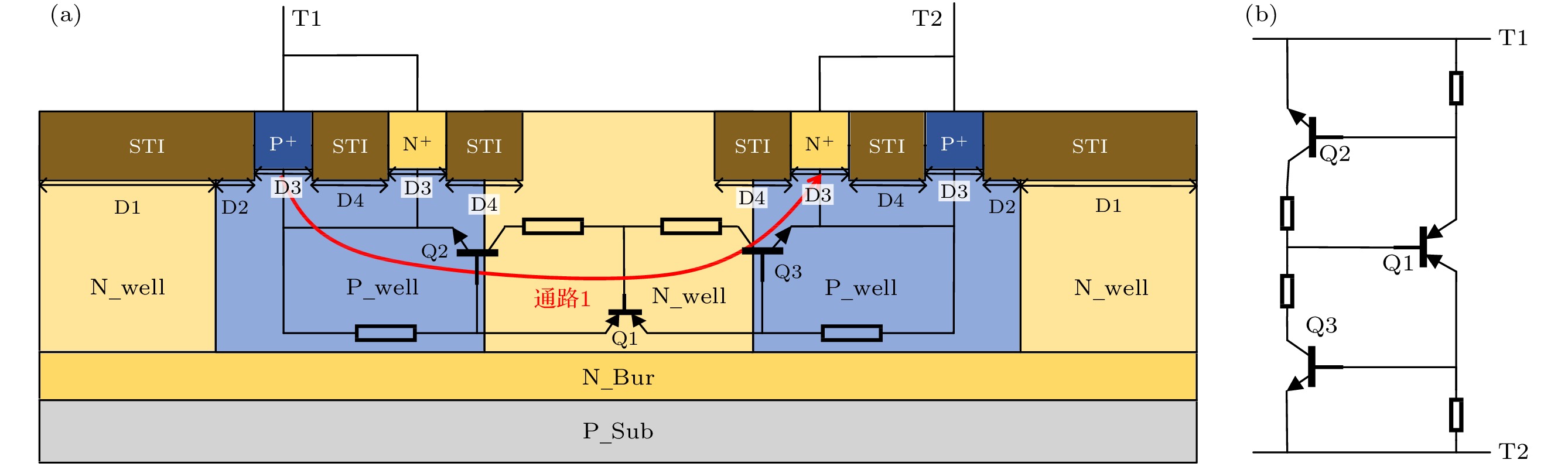
图 2 DDSCR器件结构剖面图与等效电路图
Figure 2. Structural cross-section and equivalent circuit diagram of DDSCR device.
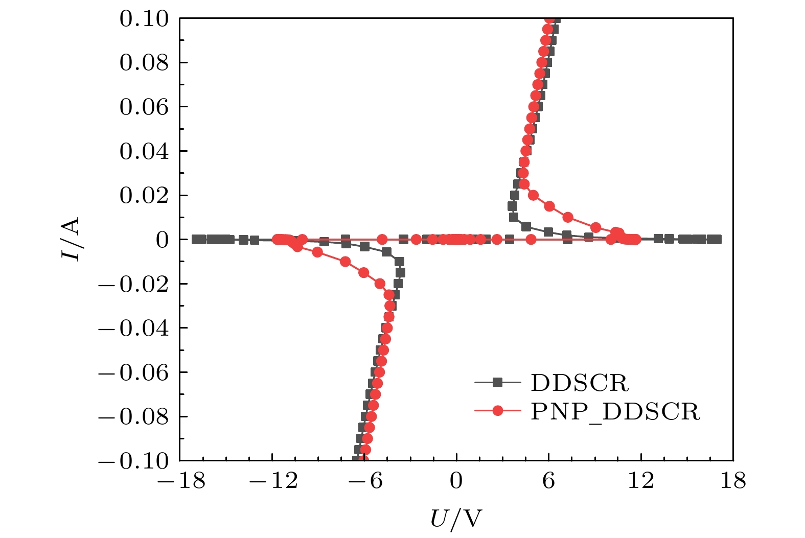
图 3 DDSCR与PNP_DDSCR的TLP仿真测试I-V曲线对比
Figure 3. Comparison of TLP simulation test I-V curves between DDSCR and PNP_DDSCR.
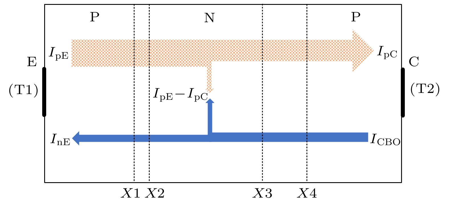
图 4 内嵌PNP晶体管电流传输示意图
Figure 4. Schematic diagram of embedded PNP transistor current transmission.

图 5 PNP_DDSCR器件T1端子施加不同应力TLP电流时的电压响应
Figure 5. Voltage response of PNP_DDSCR device T1 terminal when TLP current with different stress is applied.
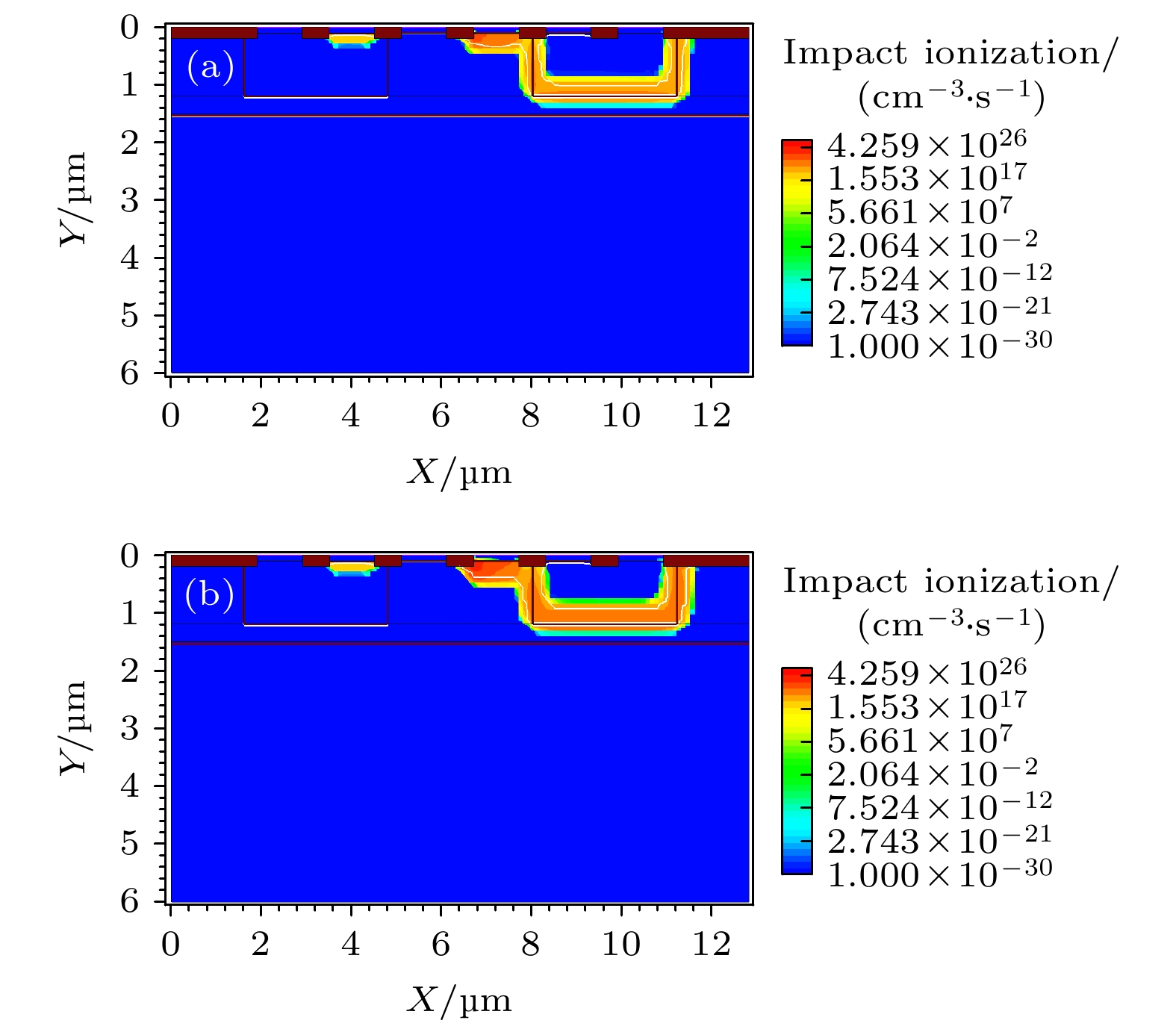
图 6 PNP_DDSCR器件碰撞电离分布图 (a) T1端子应力为2×10⁻⁷A TLP电流; (b) T1端子应力为3×10⁻⁷ A TLP电流
Figure 6. Impact ionization distribution diagram of PNP_ DDSCR device: (a) T1 terminal stress is 2×10⁻⁷ A TLP current; (b) T1 terminal stress is 3×10⁻⁷ A TLP current.
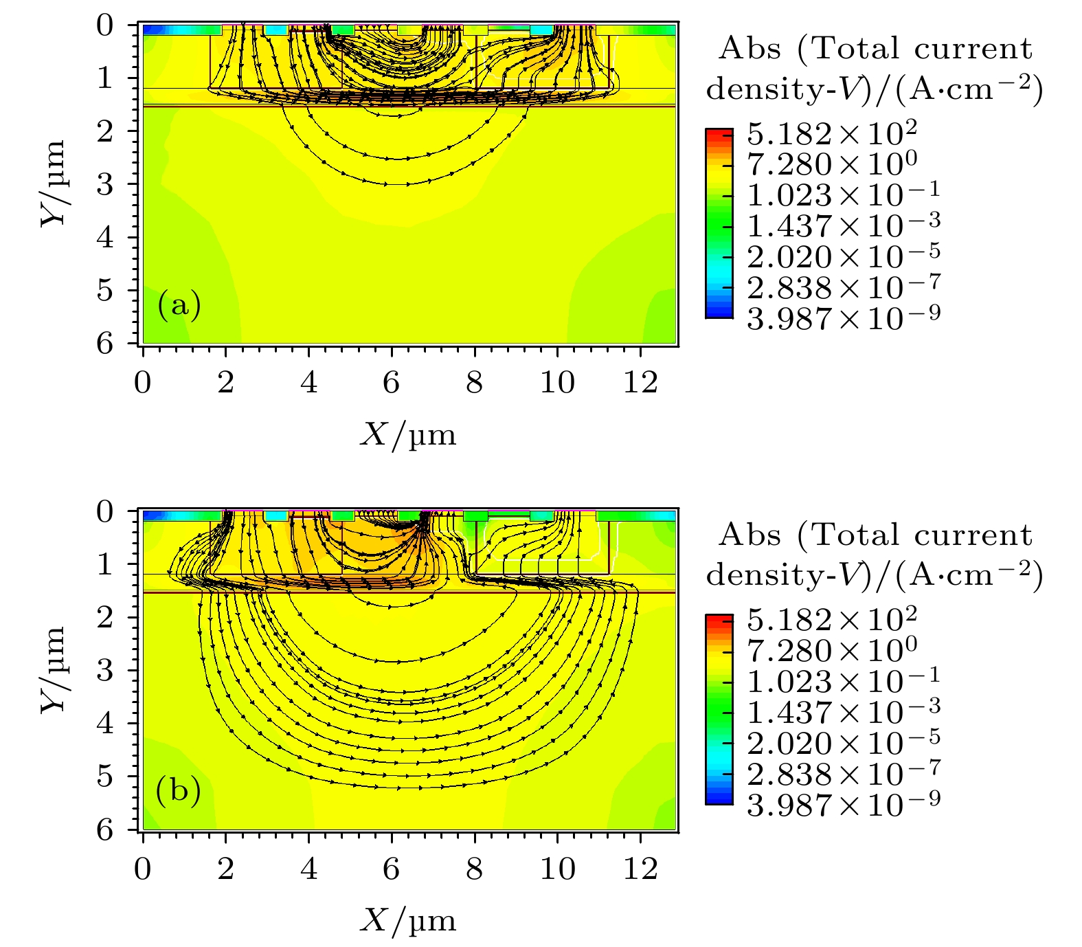
图 7 PNP_DDSCR器件电流密度分布图 (a) T1端子应力为2×10⁻⁷ A TLP电流; (b) T1端子应力为3×10⁻⁷ A TLP电流
Figure 7. Current density distribution diagram of PNP_ DDSCR device: (a) T1 terminal stress is 2×10⁻⁷ A TLP current; (b) T1 terminal stress is 3×10⁻⁷ A TLP current.
图 8 T1端子应力为0.08 A TLP电流的电流密度分布图 (a) DDSCR器件电流密度分布图; (b) PNP_DDSCR电流密度分布图
Figure 8. Current density distribution diagram of 0.08 A TLP current at T1 terminal: (a) Current density distribution diagram of DDSCR device; (b) current density distribution diagram of PNP_DDSCR device.
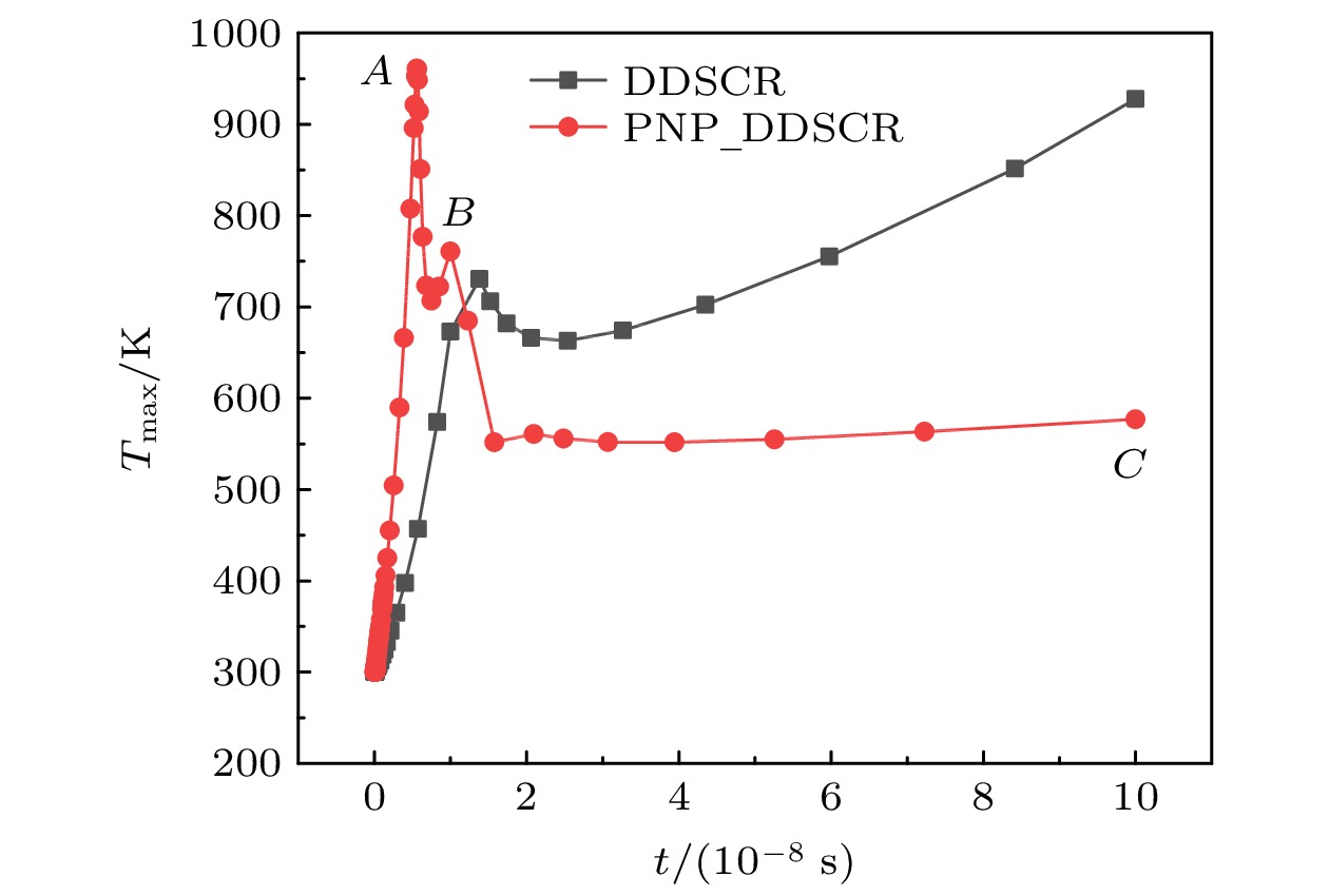
图 9 T1端子应力为2.68 A TLP电流的最高温度随时间的变化过程对比图
Figure 9. The temperature changing processes with time for T1 TLP stress of 2.68 A.
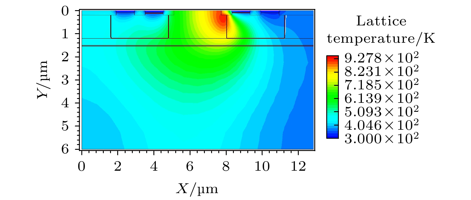
图 10 DDSCR器件温度分布图
Figure 10. Temperature distribution diagram of DDSCR device.
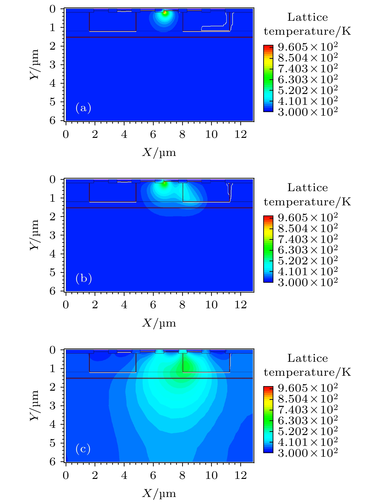
图 11 图9中三点PNP_DDSCR器件导通过程温度分布图 (a) A点; (b) B点; (c) C点
Figure 11. Temperature distribution of PNP _ DDSCR device at different point in Fig.9: (a) Point A; (b) point B; (c) point C.
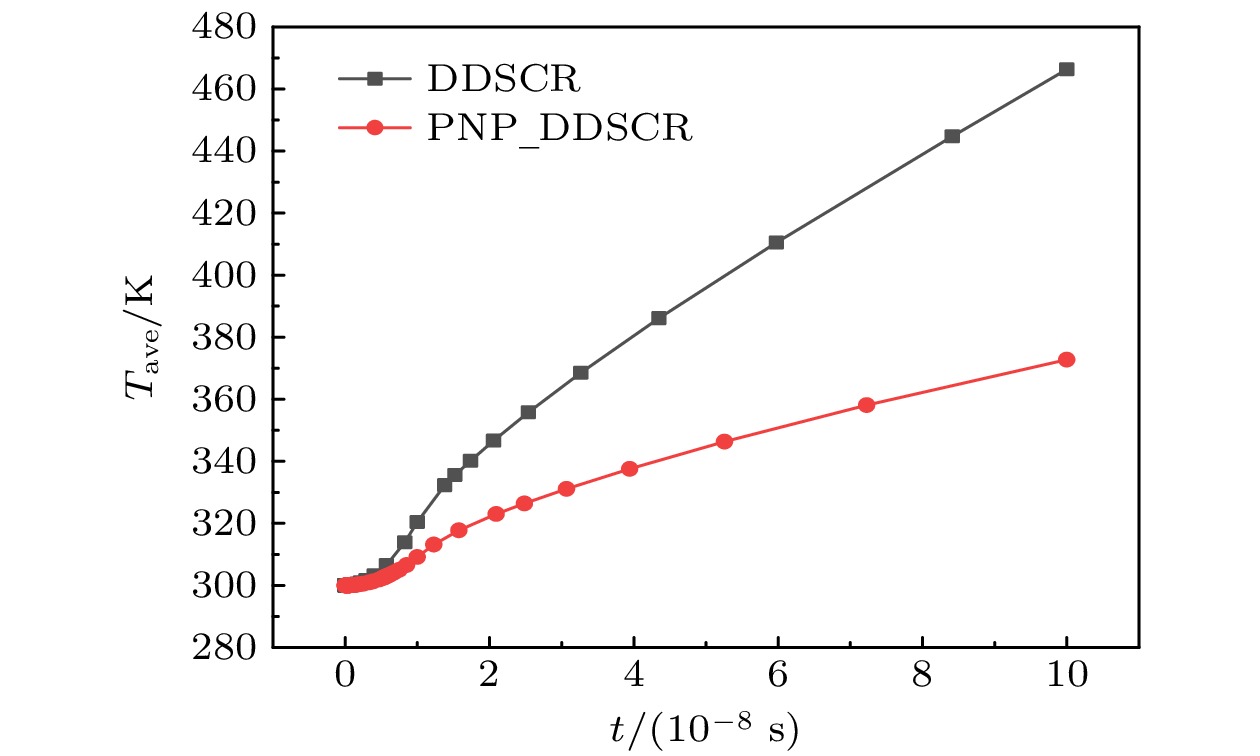
图 12 T1端子应力为2.68 A TLP电流的单位面积平均温度随时间的变化过程对比图
Figure 12. The change processes of average temperature per unit area with time when T1 TLP stress is 2.68 A.
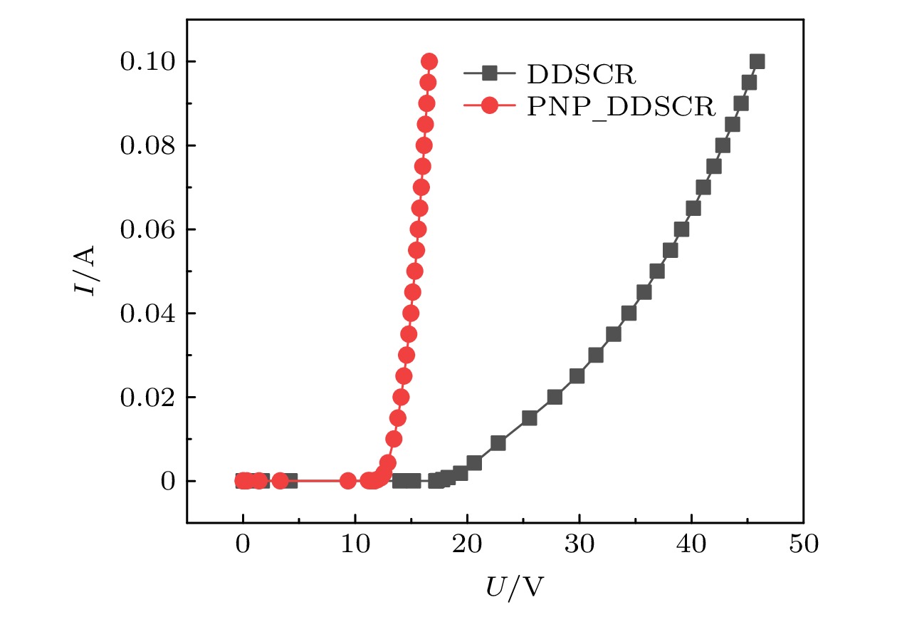
图 13 电流-过冲电压曲线对比图
Figure 13. Comparison of current-overshoot voltage curve.
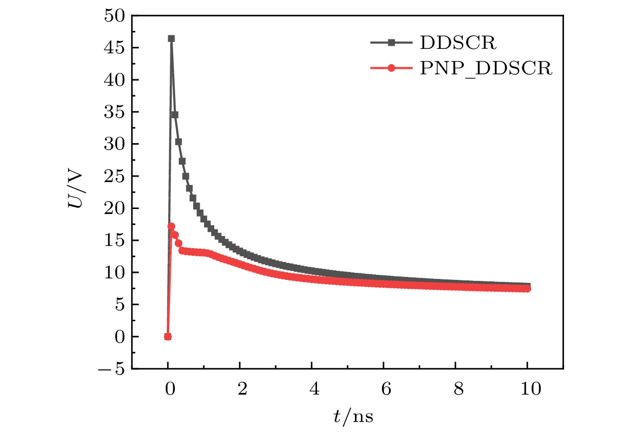
图 14 0.1 A VF-TLP响应过程对比图
Figure 14. Comparison of VF-TLP response process at 0.1 A.
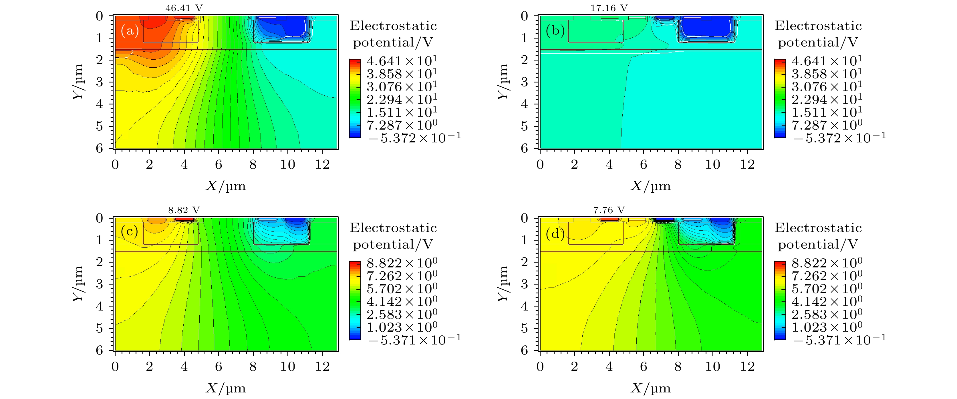
图 15 0.1 A VF-TLP脉冲强度不同时刻电势分布图 (a) 1×10⁻¹⁰ s时刻DDSCR电势分布图; (b) 1×10⁻¹⁰ s时刻PNP_DDSCR电势分布图; (c) 8×10⁻⁹ s时刻DDSCR电势分布图; (d) 8×10⁻⁹ s时刻PNP_DDSCR电势分布图
Figure 15. Potential distribution diagram of 0.1 A VF-TLP pulse intensity at different times: (a) DDSCR potential distribution diagram at 1×10⁻¹⁰ s; (b) potential distribution diagram of PNP_DDSCR at 1×10⁻¹⁰ s; (c) DDSCR potential distribution diagram at 8×10⁻⁹ s; (d) potential distribution diagram of PNP_DDSCR at 8×10⁻⁹ s.
表 1 PNP_DDSCR的关键尺寸表
Table 1. Critical dimensions of PNP_ DDSCR.
名称 尺寸/μm DDSCR PNP_DDSCR D1 1.6 1.6 D2 0.3 0.3 D3 1.0 1.0 D4 0.6 0.6  DownLoad: CSV
表 2 掺杂浓度参数表
Table 2. Doping profile.
区域(Layer) 掺杂类型 掺杂浓度/cm–3 P_Sub Boron 1×10¹⁶ N_Bur Phosphorus 1×10¹⁹ P_Well Boron 1×10¹⁷ N_Well Phosphorus 1×10¹⁷ N+ Phosphorus 1×10²⁰ P+ Boron 1×10²⁰
DownLoad: CSV
-
[1] Zhou Z J, Jin X L 2017 IEEE Electrical Design of Advanced Packaging and Systems Symposium (EDAPS) Hangzhou, China, December 14–16, 2017 p1
[2] Do K I, Lee B S, Chae H G, Seo J J, Koo Y S 2018 2nd European Conference on Electrical Engineering and Computer Science (EECS) Bern, Switzerland, December 20–22, 2018 p524
[3] Zhou Z J, Jin X L, Wang Y, Dong P 2019 IEEE 13th International Conference on ASIC (ASICON) Chongqing, China, October 29th-November 1st, 2019 p1
[4] Du F B, Liu Z W, Liu J Z, Wang J, Liou J J 2019 IEEE Trans. Device Mater. Rel. 19 169
Google Scholar
[5] Da W L, Gijs d R, Wei J T, Theo S, Albert J H 2018 IEEE Electron Device Lett. 39 331
Google Scholar
[6] Do K I, Lee B S, Koo Y S 2019 IEEE J. Electron Devi. 7 601
Google Scholar
[7] Do K I, Song B B, Koo Y S 2020 IEEE Trans. Electron Devi. 67 5020
Google Scholar
[8] Zhu L, Liang H L, Gu X F, Xu J 2020 Chin. Phys. B 29 652
Google Scholar
[9] Qi Z, Qiao M, He Y T, Zhang B 2017 Chin. Phys. B 26 350
Google Scholar
[10] Huang C Y, Chen Q K, Chi J F, Huang T H 2021 IEEE Trans. Device Mater. Rel. 21 64
Google Scholar
[11] Du F B, Hou F, Song W Q, Chen L, Nie Y L, Qing Y H, Xu Y C, Liu J Z, Liu Z W, Liou J J 2020 IEEE Trans. Electron Devi. 67 576
Google Scholar
[12] Du F B, Chang K C, Lin X N, Hou F, Zhang Y X, Han A R, Luo X, Liu Z W 2022 IEEE Trans. Electron Devi. 69 3490
Google Scholar
[13] Do K I, Koo Y S 2020 IEEE J. Electron Devi. 8 635
Google Scholar
[14] Wu M, Chen Z J 2021 9th International Symposium on Next Generation Electronics (ISNE) Changsha, China, July 9–11, 2021 p1
[15] Zeng J, Dong S R, Liou J J, Han Y, Zhong L, Wang W H 2015 IEEE Trans. Electron Devi. 62 606
Google Scholar
[16] Du F B, Jiang G J, Huang M C, Zou K P, Hou F, Song W Q, Liu J Z, Xiong X L, Hou L L, Liu Z W, Liou J J 2021 IEEE Trans. Electron Devi. 68 6338
Google Scholar
[17] Liu J Z, Liu Y L, Han A R, Nie Y L, Huang Q P, Liu Z W 2022 IEEE Trans. Electron Devi. 69 2534
Google Scholar
[18] Zhou Z J, Jin X L, Wang Y, Dong P 2021 Chin. Phys. B 30 610
Google Scholar
[19] Wang Y, Jin X L, Peng Y, Luo J, Yang J, Zheng Z W, Jiang L Y, Zhong Z Y 2021 IEEE J. Emerg. Sel. Topics Power Electron. 9 994
Google Scholar
[20] De R, Gijs 2018 IEEE J. Electron Devices Soc. 6 1097
Google Scholar
[21] 施敏, 伍国珏 著 (耿莉, 张瑞智 译) 2008 半导体器件物理 (第3版) (西安: 西安交通大学出版社) 第187—201, 415—434页
Simon M, Kork K(translated by Geng L, Zhang R Z) 2008 Physics of Semiconductor Devices (3rd Ed.) (Xi’an: Xi’an Jiaotong University Press) pp187–201, 415–434(in Chinese)
[22] 约瑟夫 L, 海因里希 S, 乌维 S, 里克 D D著 (卞抗, 杨莹, 刘静, 蒋荣舟 译) 2019 功率半导体器件-原理、特性和可靠性 (第2版) (北京: 机械工业出版社) 第248—254页
Josef L, Heinrich S, Uwe S, Rik D D (translated by Bian K, Yang Y, Liu J, Jiang R Z) 2019 Semiconductor Power Devices: Physics, Characteristics, Reliability (2nd Ed.) (Beijing: China Machine Press) pp248–254 (in Chinese)
[23] Chen Q, Ma R, Zhang W, Lu F, Wang C K, Liang O, Zhang F L, Li C, Tang H, Xie Y H, Wang A 2016 IEEE Trans. Electron Devi. 63 3205
Google Scholar

 DownLoad:
Catalog
Metrics
- Abstract views: 2758
- PDF Downloads: 55
- Cited By: 0
