


The 90th Anniversary of Acta Physica Sinica

VIEWS AND PERSPECTIVES
2024, 73 (1): 010301.
doi: 10.7498/aps.73.20231795
Abstract +
In the early decades of the 20th century, the inception of quantum mechanics catalyzed the first quantum revolution, resulting in groundbreaking technological advances, such as nuclear energy, semiconductors, lasers, nuclear magnetic resonance, superconductivity, and global satellite positioning systems. These innovations have promoted significant progress in material civilization, fundamentally changed the way of life and societal landscape of humanity. Since the 1990s, quantum control technology has made significant strides forward, ushering in a rapid evolution of quantum technologies, notably exemplified by quantum information science. This encompasses domains such as quantum communication, quantum computing, and quantum precision measurement, offering paradigm-shifting solutions for enhancing information transmission security, accelerating computational speed, and elevating measurement precision. These advances hold the potential to provide crucial underpinning for national security and the high-quality development of the national economy. The swift progression of quantum information technology heralds the advent of the second quantum revolution. Following nearly three decades of concerted efforts, China’s quantum information technology field as a whole has achieved a leap. Specifically, China presently assumes a prominent international role in both the research and practical application of quantum communication, leading the global domain in quantum computing, and achieving international preeminence or advanced standing across various facets of quantum precision measurement. Presently, it is imperative to conduct a comprehensive assessment of the developmental priorities in the realm of quantum information in China for the forthcoming 5 to 10 years, in alignment with national strategic priorities and the evolving landscape of international competition. This will enable the proactive establishment of next-generation information technology systems that are secure, efficient, autonomous, and controllable.


EDITOR'S SUGGESTION
2024, 73 (1): 017503.
doi: 10.7498/aps.73.20231940
Abstract +
Diluted ferromagnetic semiconductors (DMSs) have attracted widespread attention in last decades, owing to their potential applications in spintronic devices. But classical group-III-IV, and -V elements based DMS materials, such as (Ga,Mn)As which depend on heterovalent (Ga3+, Mn2+) doping, cannot separately control carrier and spin doping, and have seriously limited chemical solubilities, which are disadvantages for further improving the Curie temperatures. To overcome these difficulties, a new-generation DMS with independent spin and charge doping have been designed and synthesized. Their representatives are I-II-V based Li(Zn,Mn)As and II-II-V based (Ba,K)(Zn,Mn)2As2. In these new materials, doping isovalent Zn2+ and Mn2+ introduces only spins, while doping heterovalent non-magnetic elements introduces only charge. As a result, (Ba,K)(Zn,Mn)2As2 achieves Curie temperature of 230 K, a new record among DMS where ferromagnetic orderings are mediated by itinerate carriers. Herein, we summarize the recent advances in the new-generation DMS materials. The discovery and synthesis of several typical new-generation DMS materials are introduced. Physical properties are studied by using muon spin relaxation, angle-resolved photoemission spectroscopy and pair distribution function. The physical and chemical pressure effects on the title materials are demonstrated. The Andreev reflection junction based on single crystal and the measurement of spin polarization are exhibited. In the end, we demonstrate the potential multiple-parameter heterojunctions with DMSs superconductors and antiferromagnetic materials.
SPECIAL TOPIC—Two-dimensional magnetism and topological spin physics
VIEWS AND PERSPECTIVES
Coupling between magnetism and topology: From fundamental physics to topological magneto-electronics
2024, 73 (1): 017103.
doi: 10.7498/aps.73.20231711
Abstract +
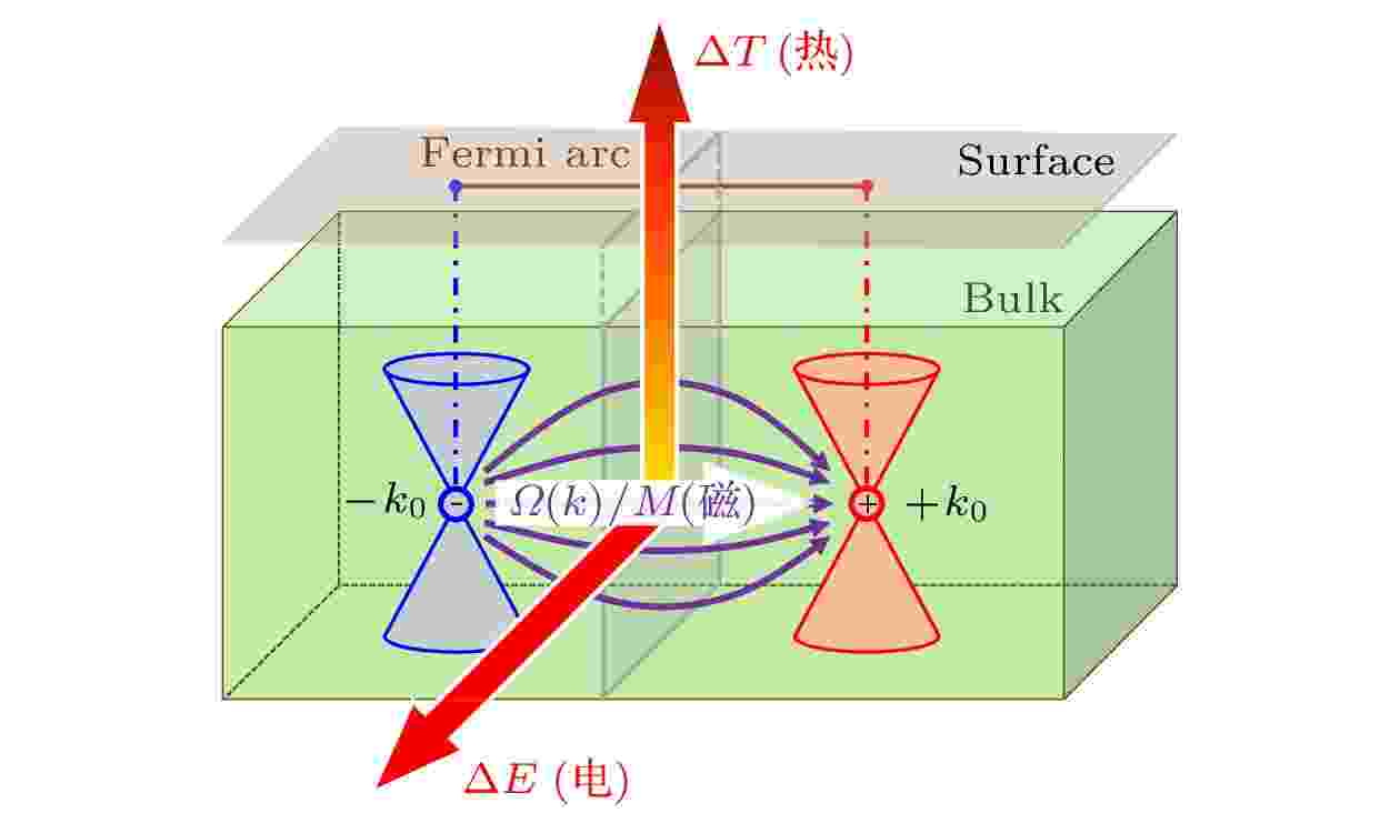
Magnetism and topological physics are both well-developed disciplines, and their combination is a demand and foundation for the development of next-generation magneto-electronics. Magnetic topological materials are important products of coupling between magnetic order and topological physics, providing material carrier and regulatory degrees of freedom for novel topological physics. Magnetic Weyl semimetals realize Weyl fermion states under time-reversal symmetry breaking, leading to a host of novel magnetic, electric, thermal, and optical effects through enhanced Berry curvature originating from topology. The interaction between Weyl electrons and magnetic order also establishes topological electronic physics as a new principle and driving force for magneto-electronic applications. At present, the primary task and characteristic of the first development stage of magnetic topological materials is to discover new states and effects, while the understanding of interaction between topologically nontrivial electrons in momentum space and magnetic order in real space has received attention of researchers. The comprehensive advances of these two stages will accumulate the physical foundation and application explorations for topological magneto-electronics. This paper focuses on the two development stages of magnetic topological materials and discusses three aspects: (i) proposal and realization of strategy for magnetic topological materials; (ii) exploration of electronic states with nontrivial topology under uniform magnetic order and their associated novel physical properties; (iii) the interaction between localized magnetic states and topological electrons. It provides an in-depth discussion on current hot topics and development trends in the field, and future development in topological magneto-electronics, thereby assisting in the future development of topological spin quantum devices.

2024, 73 (1): 017502.
doi: 10.7498/aps.73.20231244
Abstract +
The rapid development of information technology has put forward higher requirements for the performance of information processing and storage devices. At the same time, with the continuous reduction of device size, traditional semiconductor devices based on electron charge properties face the problems and challenges of thermal dissipation and quantum size effect, and semiconductor technology has entered the post-molar era. Unlike traditional charge-based electronic devices, spin-based non-volatile spintronic devices not only have high integrated density, read and write speed and read and write time, but also can effectively avoid heat dissipation, establishing a new technical platform for developing the information storage, processing and communication. In recent years, two-dimensional materials have attracted a lot of attention due to their unique band structures and rich physical properties. Two-dimensional magnetic materials have shown great research and application potential in the field of spintronics. Compared with traditional block materials, the two-dimensional materials can provide great opportunities for exploring novel physical effects and ultra-low-power devices due to their atomic thickness, ultra-clean interface and flexible stacking. At the same time, with the rise of topological materials (TMs), their topological protected band structures, diversified crystal structures and symmetries, strong spin-orbit coupling and adjustable electrical conductivity provide an ideal physical research platform for studying spintronics. In this paper, we first introduce the common methods of preparing two-dimensional materials, then focus on the research progress of two-dimensional magnetic materials in the field of spin-orbit electronics, and finally look forward to the research challenges in this field. In the future, with continuous in-depth research on the preparation, physical properties and device applications of two-dimensional magnetic materials, two-dimensional magnetic materials will show more extensive research prospects and application value in the field of spintronics. Two-dimensional magnetic materials will provide more material systems for spintronics development.

2024, 73 (1): 017504.
doi: 10.7498/aps.73.20231612
Abstract +
Topological magnetic skyrmions, as information units, possess distinct advantages such as high reliability, enhanced integration, and low energy consumption. These novel topological characteristics offer critical material and technological support for the rapid development of information technology, 5G communication, and big data. However, the application of magnetic skyrmions in practical devices is severely impeded by certain limitations, including their stability dependence on magnetic field and the deflection caused by the skyrmion Hall effect under electric current. Consequently, exploring new topological magnetic domain structures and material systems suitable for application becomes a pivotal area of research. This paper primarily focuses on experimental studies utilizing high-resolution Lorentz transmission electron microscopy for in situ real-space observation and manipulation of topological merons and skyrmions inside the magnetic domain wall, confirming the theoretical prediction of magnetic domain wall skyrmions in 2013. We has firstly achieved topological meron chains inside the domain walls by using the spin reorientation transition in two-dimensional van der Waals Fe5–xGeTe2 magnets, and systematically studied the dynamic behavior of domain wall topological magnetic domain structures under external electric and magnetic fields, filling the blanks in this research area. The important and special roles of magnetic domain walls are revealed at the same time. Then the GdFeCo amorphous ferrimagnetic thin film was designed and prepared based on the summarized mechanism with the domain wall meron pairs successfully reproduced. Moreover, the reversible topological transformation from domain wall meron pair to domain wall skyrmions has also been realized without external magnetic field during spin reorientation transformation as temperature changing. The results of micromagnetic simulation and electric experiments on the topological domains in domain walls would provided a strong basis and support for the future research.

2024, 73 (1): 017505.
doi: 10.7498/aps.73.20231166
Abstract +
Novel quantum materials such as topological materials, two-dimensional materials, create new opportunities for the spintronic devices. These materials can improve the charge-spin conversion efficiency, provide high-quality interface, and enhance the energy efficiency for spintronic devices. In addition, they have rich interactions and coupling effects, which provides a perfect platform for finding new physics and novel methods to control the spintronic properties. Many inspiring results have been reported regarding the research on topological materials and two-dimensional materials, especially the layered topological and two-dimensional magnetic materials, and their heterostructures. This paper reviews the recent achievements of these novel quantum materials on spintronic applications. Firstly the breakthroughs that topological materials have been made in spin-orbit torque devices is introduced, then two-dimensional magnetic materials and their performances in spintronic devices are presented, finally the research progress of topological materials/two-dimensional magnetic materials heterostructures is discussed. This review can help to get a comprehensive understanding of the development of these novel quantum materials in the field of spintronics and inspire new ideas of research on these novel materials.

2024, 73 (1): 018501.
doi: 10.7498/aps.73.20231836
Abstract +
The Wely semimetal WTe2 exhibits significant spin-orbit coupling characteristics and can generate unconventional spin current with out-of-plane polarization, which has become a hotspot in recent years. Meanwhile, WTe2 also has high charge-spin conversion efficiency, allowing perpendicular magnetization to be switched deterministically without the assistance of an external magnetic field, which is critical for the high-density integration of low-power magnetic random-access memories. The purpose of this paper is to review the recent advances in the research on spin orbit torque in heterostructures composed of WTe2 and ferromagnetic layers, focusing on progress of research on the detection and magnetization switching in the spin orbit torque of heterojunctions composed of WTe2 prepared by different methods (e.g. mechanical exfoliation and chemical vapor deposition) and ferromagnetic layers such as conventional magnets (e.g, FeNi and CoFeB, etc.) and two-dimensional magnets (e.g. Fe3GeTe2, etc.). Finally, the prospect of related research is discussed.

2024, 73 (1): 011201.
doi: 10.7498/aps.73.20231473
Abstract +
Magnetic skyrmion is a kind of nontrivial topological magnetic structure, which can exist stably in chiral magnet with Dzyaloshinskii-Moriya (DM) interaction, and its static and dynamic properties are closely related to its structural characteristics. However, there are no general analytical expressions for skyrmion profiles. Therefore, many researchers have provided approximate solutions. In this paper, a new approach to exploring magnetic skyrmion structures is introduced by using a symbolic regression approach. Considering the influence of DM interaction and external magnetic field on magnetic skyrmion structure, two suitable approximate expressions are obtained through symbolic regression algorithms. The applicability of these expressions depends on the dominant interaction. The research results in this work validate the powerful capability of symbolic regression algorithms in exploring the magnetic skyrmion profiles. So, the present study provides a new method for finding the analytical expressions for magnetic structure.
SPECIAL TOPIC—Two-dimensional magnetism and topological spin physics • COVER ARTICLE

COVER ARTICLE
2024, 73 (1): 017501.
doi: 10.7498/aps.73.20231589
Abstract +
Hall effect is an ancient but highly potential subfield in condensed matter physics, and its origin can be traced back hundreds of years. In 1879, Hall made a momentous discovery that when a current-carrying conductor is placed in a magnetic field, the Lorentz force pushes its electrons to one side of the conductor. This intriguing phenomenon was dubbed Hall effect. Since then, a series of novel Hall effects have been discovered, including anomalous Hall effect, quantum Hall effect, spin Hall effect, topological Hall effect, and planar Hall effec. Notably, Hall effects play an important role in realizing the information transport, since it can realize the mutual conversion of current in different directions. In bosonic systems such as magnons, a series of magnon Hall effects have been found, jointly driving the development of the magnon-based spintronics. In this perspective, we review the researches of the Hall effect in magnonic system in recent years, and briefly introduce its modern semi-classical theories, including virtual electromagnetic field theory and scattering theory. Furthermore, we introduce the different magnon Hall effects and clarify the physics behind them. Finally, the prospect of magnon Hall effect is discussed.
GENERAL

EDITOR'S SUGGESTION
2024, 73 (1): 010401.
doi: 10.7498/aps.73.20231233
Abstract +
In this paper, we discuss the influence of thin disk accretion and asymptotically safe (AS) gravity correction parameters on the shadow and photon ring of black hole. For the thin disk accretion, the dark region is the shadow of the black hole, and the bright photon ring is composed of direct image, lensing ring, and photon ring. For the specific intensity of the radiation source of the accretion disk, we consider three different emission profile models. For the second-order attenuation function model in which the emission starts from the innermost circular orbit, direct image, lensing ring, and photon ring can be clearly distinguished. The direct image contributes most of the brightness, and the lensing ring contributes a small portion, while the contribution of the photon ring can almost be ignored. And the observed corresponding intensity peak decreases with the increase of the AS gravity parameter, that is, the corresponding brightness of the photon ring darkens as correction parameter increases. For the third-order attenuation function model in which the emission begins at the radius of the photon sphere, lensing ring and photon ring are superimposed on the direct radiation. Thus a new extreme value of the observed intensity emerges, and the extreme value increases with the increase of the AS gravity parameter, which leads to a brighter observed photon ring. For the anti-trigonometric attenuation function model in which the radiation starts from the event horizon, the superposition range of lensing ring and photon ring on the direct radiation becomes larger, which makes photon ring wider. The smaller the AS gravity parameter, the more difficult it is to distinguish between the lensing ring and photon ring, and the brighter the photon ring turns. In short, the results show that the shadow radius decreases with the increase of the AS correction parameter. For different AS gravity correction parameters, the light intensities of emission source, especially emission profiles of the observed intensity are significantly different, resulting in obvious differences in observed emission intensity between the shadow of the black hole and the bright photon ring of the black hole.

2024, 73 (1): 010501.
doi: 10.7498/aps.73.20231211
Abstract +
A physical memristor has an asymmetric tight hysteresis loop. In order to simulate the asymmetric tight hysteresis curve of the physical memristor more conveniently, a fractional-order diode bridge memristor model with a bias voltage source is proposed in this paper, which can continuously regulate the hysteresis loop. Firstly, based on fractional calculus theory, a fractional order model of a diode bridge memristor with a bias voltage source is established, and its electrical characteristics are analyzed. Secondly, by integrating it with the Jerk chaotic circuit, a non-homogeneous fractional order memristor chaotic circuit model with a bias voltage source is established, and the influence of bias voltage on its system dynamic behavior is studied. Once again, a fractional-order equivalent circuit model is built in PSpice and validated through circuit simulation. The experimental results are basically consistent with the numerical simulation results. Finally, the experiments on the circuit are completed in LabVIEW to validate the correctness and feasibility of the theoretical analysis. The results indicate that the fractional order memristor with bias voltage source can continuously obtain asymmetric tight hysteresis loop by adjusting the voltage of the bias voltage source. As the bias power supply voltage changes, the non-homogeneous fractional order memristor chaotic system exhibits that the period doubling bifurcation turns into chaos due to the symmetry breaking.

2024, 73 (1): 010701.
doi: 10.7498/aps.73.20231246
Abstract +
Two-dimensional (2D) ferroelectric materials are important materials for both fundamental properties and potential applications. Especially, group Ⅳ monochalcogenide possesses highest thermoelectric performance and intrinsic ferroelectric polarization properties and can sever as a model to explore ferroelectric polarization properties. However, due to the relatively large exfoliation energy, the creation of high-quality and large-size monolayer group Ⅳ monochalcogenide is not so easy, which seriously hinders the integration of these materials into the fast-developing field of 2D materials and their heterostructures. Herein, monolayer GeS is successfully fabricated on Cu(111) substrate by molecular beam epitaxy method, and the lattice structure and the electronic band structure of monolayer GeS are systematically characterized by high-resolution scanning tunneling microscopy, low-energy electron diffraction, in-situ X-ray photoelectron spectroscopy, Raman spectra, and angle-resolved photoelectron spectroscopy, and density functional theory calculations. All atomically resolved STM images reveal that the obtained monolayer GeS has an orthogonal lattice structure, which consists with theoretical prediction. Meanwhile, the distinct moiré pattern formed between monolayer GeS and Cu(111) substrate also confirms the orthogonal lattice structure. In order to examine the chemical composition and valence state of as-prepared monolayer GeS, in-situ XPS is utilized without being exposed to air. The measured spectra of XPS core levels suggest that the valence states of Ge and S elements are identified to be +2 and –2, respectively and the atomic ratio of Ge/S is 1∶1.5, which is extremely close to the stoichiometric ratio of 1∶1 for GeS. To further corroborate the quality and lattice structure of the monolayer GeS film, ex-situ Raman measurements are also performed for monolayer GeS on highly oriented pyrolytic graphene (HOPG) and multilayer graphene substrate. Three well-defined typical characteristic Raman peaks of GeS are observed. Finally, in-situ ARPES measurement are conducted to determine the electronic band structure of monolayer GeS on Cu(111). The results demonstrate that the monolayer GeS has a nearly flat band electronic band structure, consistent with our density functional theory calculation. The realization and investigation of the monolayer GeS extend the scope of 2D ferroelectric materials and make it possible to prepare high quality and large size monolayer group Ⅳ monochalcogenides, which is beneficial to the application of this main group material to the rapidly developing 2D ferroelectric materials and heterojunction research.
ATOMIC AND MOLECULAR PHYSICS

2024, 73 (1): 013101.
doi: 10.7498/aps.73.20231236
Abstract +
As is well known, the leakage of four toxic gases, NO2, NH3, mustard gas and sarin greatly threaten the environment and human health. Among of them, mustard gas and sarin are two serious chemical and biological weapons agents, and exposure to a small amount can cause skin burns and immediate death. NO2 and NH3 are two common toxic pollutants produced by automobile exhaust, coal combustion and petrochemical industry. The presence of trace amounts of NO2 and NH3 gas in human tissues can cause serious respiratory diseases and damage human brain and other systems. Thus, it is very important to realize the rapid detection of NO2, NH3, mustard gas and sarin in academia and industry. In this study, we use density functional theory to investigate the ability of a transition metal Mo doped two-dimensional VS2 structure to detect the four representative toxic gases. The results reveal that Mo atom doping has a significant effect on the stability and gas-sensitivity of the VS2 structure. The Mo atom can be successfully doped on the S-vacancy in the two-dimensional VS2 structure. Compared with the undoped structure VS2, the doped structure Mo-VS2 has strong interaction with NO2, NH3, sarin, and mustard gas, realizing effective adsorption of them. The presence of Mo atom in the VS2 lattice changes the electronic structure of VS2, also modifies its band gap and density of states. The interaction between the Mo-VS2 structure and the target analytes depends strongly on the nature of the gas molecule. The binding energy values for NO2, NH3, mustard gas, and sarin on the Mo-VS2 are significantly higher than those on the pristine VS2, indicating stronger interaction between the Mo-VS2 structure and these gases. Our calculations show that the Mo atom in VS2 changes its electrical resistance after being exposed to the gases, which can be used to distinguish different gases. Moreover, differences in charge redistribution within the Mo-VS2 structure upon being exposed to different gases can be used to explain their differential gas-sensitivity. Our results can provide sufficient theoretical basis for experimental researchers to design and optimize the performances of sensors in practical applications.

2024, 73 (1): 013701.
doi: 10.7498/aps.73.20231243
Abstract +
Efficient preparation of cold atoms plays an important role in realizing precision measurement including optical lattice clocks (OLCs). Fast preparation of cold atoms reduces Dick noise by shortening dead time in a clock interrogation cycle, which improves the stability of OLCs. Here, we increase the loading rate of the three-dimensional magneto-optical trap (3D-MOT) in the ultra-high vacuum environment by utilizing the two-dimensional magneto-optical trap (2D-MOT) with a push beam, reduce the temperature of cold atoms with the compression-MOT technique which is implemented by reducing the detuning of 3D-MOT rapidly at the end of atom preparation, and realize the enhanced production of cold atoms for 199Hg OLCs. To achieve 3D-MOT and 2D-MOT of mercury atoms, a deep ultraviolet laser (DUVL) system composed of three DUVLs is developed with one working in lower power for frequency locking and the other two in high power for laser cooling. Such a configuration improves the long-term frequency stability and shows greater robustness than our previous system consisting of two DUVLs. To maximize the 3D-MOT loading rate, we orderly optimize the detuning and the magnetic field gradient of 3D-MOT and those of 2D-MOT as well as the detuning and the power of the push beam. After all parameters are optimized, we measure the maximum loading rate of 3D-MOT to be 3.1×10⁵ s–1 and prepare cold atoms of 1.8×10⁶ in 9 s. The loading rate is greatly enhanced by a factor of 51 by using 2D-MOT and the push beam. In order to improve the efficiency of transferring cold atoms from 3D-MOT to optical lattice, we use compression-MOT technique to reduce the temperature of cold atoms and produce cold 199Hg atoms which are about 45 μK, lower than the expected temperature of Doppler cooling theory. By achieving the high gain of the 3D-MOT loading rate under the ultra-high vacuum and reducing the temperature of cold atoms, this enhanced preparation of cold atoms based on 2D-MOT effectively shortens the preparation time of cold atoms and improves the transfer efficiency of optical lattice, which provides a significant scheme for efficiently preparing cold mercury atoms in other experiments.
ELECTROMAGNETISM, OPTICS, ACOUSTICS, HEAT TRANSFER, CLASSICAL MECHANICS, AND FLUID DYNAMICS

2024, 73 (1): 014101.
doi: 10.7498/aps.73.20230653
Abstract +
In this paper, an asymmetric transmission scheme is proposed by cascading an acousto-optic device and a coupled whispering gallery mode (WGM) microsphere cavity, and it is demonstrated theoretically and experimentally. With the acousto-optic interaction in a fiber, the vector modes of the fundamental core mode can be converted into the different vector modes of a cladding (linear polarization, LP) mode, and because of the optical path difference between the cladding vector modes, the polarization of the cladding mode will be changed. The cladding mode can be converted back into the core fundamental mode by coupling a WGM microcavity. By calculating the overlapping of the mode fields in the tapered fiber and the microcavity at the resonance wavelength, the coupling coefficients between different LP modes and WGM will be solved. And, the transmitivities and conversion coefficients of the two fiber modes can be obtained on condition that the polarization of the incident light does not coincide with the polarization orientation of the WGM. The transmission spectra of the coupled WGM microcavity are calculated by using Matlab program for eight states, including the states at different incident directions, different incident polarizations of input, whether the acoustic wave is on or off. The results show that the conversion coefficient from the cladding mode to the core mode is completely different from that of the contrary process when the acoustic wave is working. And the forward incident light and backward incident light have completely different transmission characteristics, thus resulting in the asymmetric transmission. The transmittances of forward incidence and reverse incidence at different polarizations are also studied, both of them change periodically with the polarization angle, and their phase difference is equal to the polarization change caused by acousto-optic interaction in the fiber. In the experiment, a two-stage tapered fiber is used to realize the acousto-optic interaction and the coupling of whispering gallery mode at the same time. By controlling the working states of the system, the same 8 states as in the calculation are studied experimentally. The results show that due to the polarization-selection effect of the WGM, the light energy incident from the opposite directions will show different transmission characteristics. While the forward transmittance reaches a maximum value of about 0.505, the reverse transmittance reaches a minimum value of about 0.010, and the transmission isolation reaches about 17 dB. The transmittances in two directions are measured at different incident polarization angles, the transmission isolation is analyzed, and the polarization change of cladding mode in the fiber is verified to be about ${80^ \circ }$ . The measured results coincide with the calculations from the developed theory well. Finally, the shortcomings and optimization method of the scheme are discussed. The asymmetric transmission scheme in this paper inherits the advantages of rapid response and good tuning of acousto-optic device, and has an all-fiber structure, which has important application potential in optical switch and isolator.


2024, 73 (1): 014201.
doi: 10.7498/aps.73.20231212
Abstract +
Optical nonreciprocity has been a popular research topic in recent years. Semiconductor quantum wells (SQWs) play a key role in many high-performance optoelectronic devices. In this paper, we propose a theoretical scheme to achieve nonmagnetic optical nonreciprocity based on the four-wave mixing effect in SQW nanostructures. Using the experimentally available parameters, the nonreciprocal behavior of the probe field in forward direction and backward direction is achieved through this SQW, where both nonreciprocal transmission and nonreciprocal phase shift have high transmission rates. Furthermore, by embedding this SQW nanostructure into a Mach-Zender interferometer, a reconfigurable nonreciprocal device based on high transmission nonreciprocal phase shift that can be used as an isolator or a circulator, is designed and analyzed. The device can be realized as a two-port optical isolator with an isolation ratio of 92.39 dB and an insertion loss of 0.25 dB, and as a four-port optical circulator with a fidelity of 0.9993, a photon survival probability of 0.9518 and a low insertion loss with suitable parameters. Semiconductor media have the advantages of easier integration and tunable parameters, and this scheme can provide theoretical guidance for implementing nonreciprocal and nonreciprocal photonic devices based on semiconductor solid-state media.

EDITOR'S SUGGESTION
2024, 73 (1): 014202.
doi: 10.7498/aps.73.20231030
Abstract +

EDITOR'S SUGGESTION
2024, 73 (1): 014203.
doi: 10.7498/aps.73.20231278
Abstract +
Blue laser with high power and high beam quality has many applications such as in laser display, underwater communication and imaging, and non-ferrous metal processing. Optically pumped external-cavity surface-emitting laser combines the advantages of both surface-emitting semiconductor lasers and solid-state disk lasers, and can produce high output power and good beam quality simultaneously. Its high intracavity circulating power is more conducive to intracavity frequency doubling, achieving high-power and high beam quality blue light through fundamental laser in the near-infrared waveband. This paper reports an efficient intracavity frequency doubled 490 nm high power blue light by using a 980 nm fundamental laser in an external-cavity surface-emitting laser. The V-type resonant cavity is formed by the high reflectivity distributed Bragg reflector (DBR) at the bottom of gain chip, a folded flat concave mirror (high reflectivity coated for 980 nm and anti-reflectivity coated for 490 nm), and a flat concave end mirror (high reflectivity coated for 980 nm and 490 nm). By inserting a nonlinear crystal LBO into the cavity at the beam waist formed by the folded mirror and end mirror, and employing a birefringent filter (BRF) to polarize the fundamental laser and narrow the linewidth of the laser, a high power and high beam quality blue laser with high conversion efficiency is obtained. The effects of different factors including the length of nonlinear crystal, the linewidth of fundamental laser, and the compensation of walk off angle on the output power of the blue laser are studied experimentally. The length of the nonlinear crystal is optimized based on the size of the fundamental laser beam waist at the position of the crystal in the resonant cavity. Under the type-I phase matching condition of LBO, over 6 W output power at 491 nm wavelength is obtained when the crystal length is 5 mm and the BRF thickness is 1 mm. The beam quality M2 factor in the x direction and the y direction are both 1.08, and the conversion efficiency of frequency doubling is 63%. The experimental results also show that symmetrically placed nonlinear crystals can compensate for the walk-off angle during frequency doubling to a certain extent, thereby clearly improving the conversion efficiency of the frequency doubled blue laser.
EDITOR'S SUGGESTION
2024, 73 (1): 014204.
doi: 10.7498/aps.73.20231085
Abstract +
Orbital angular momentum (OAM) lasers have potential applications in large capacity communication systems, laser processing, particle manipulation and quantum optics. OAM mode femtosecond fiber laser has become the research focus due to the advantages of simple structure, low cost and high peak power. At present, OAM mode femtosecond fiber lasers have made some breakthroughs in key parameters such as repetition frequency, pulse width, spectrum width, but it is difficult to achieve good overall performance. Besides, the repetition rate is tens of MHz at present. In this paper, a large-bandwidth mode coupler is made based on the mode phase matching principle. In coupler, the first order mode coupler with 3 dB polarization dependent loss is made by the technology of strong fused biconical taper, and the second order mode coupler with 0.3 dB polarization dependent loss is made by the technology of weak fused biconical taper. By combining the nonlinear polarization rotation mode-locking mechanism, OAM mode femtosecond fiber laser with over 100 MHz repetition rate is built. The achievement of the key parameters is attributed to the selection of dispersion shifted fibers that can accurately adjust intracavity dispersion. Comparing with traditional dispersion compensation fibers (DCF), the group velocity dispersion is reduced by an order of magnitude, so it can better adjust intracavity dispersion to achieve the indexes of large spectral bandwidth and narrow pulse width. In addition, the diameter of the fiber is 8 μm, which is the same as that of a single mode fiber. Comparing with DCF, the fusion loss can be ignored, so only a shorter gain Erbium-doped fiber is required, which ensures a shorter overall cavity length and achieves high repetition frequency. The experimental results show that the first order OAM mode fiber laser has 113.6 MHz repetition rate, 98 fs half-height full pulse width, and 101 nm 10 dB bandwidth. Second-order OAM mode fiber laser has 114.9 MHz repetition rate, 60 fs half-height full pulse width, and 100 nm 10 dB bandwidth. Compared with the reported schemes, our scheme has good performance in key parameters such as repetition rate, pulse width and spectral width. We believe that the OAM mode fiber laser with excellent performance is expected to be widely used in OAM communication, particle manipulation and other research fields.
EDITOR'S SUGGESTION
2024, 73 (1): 014205.
doi: 10.7498/aps.73.20231049
Abstract +
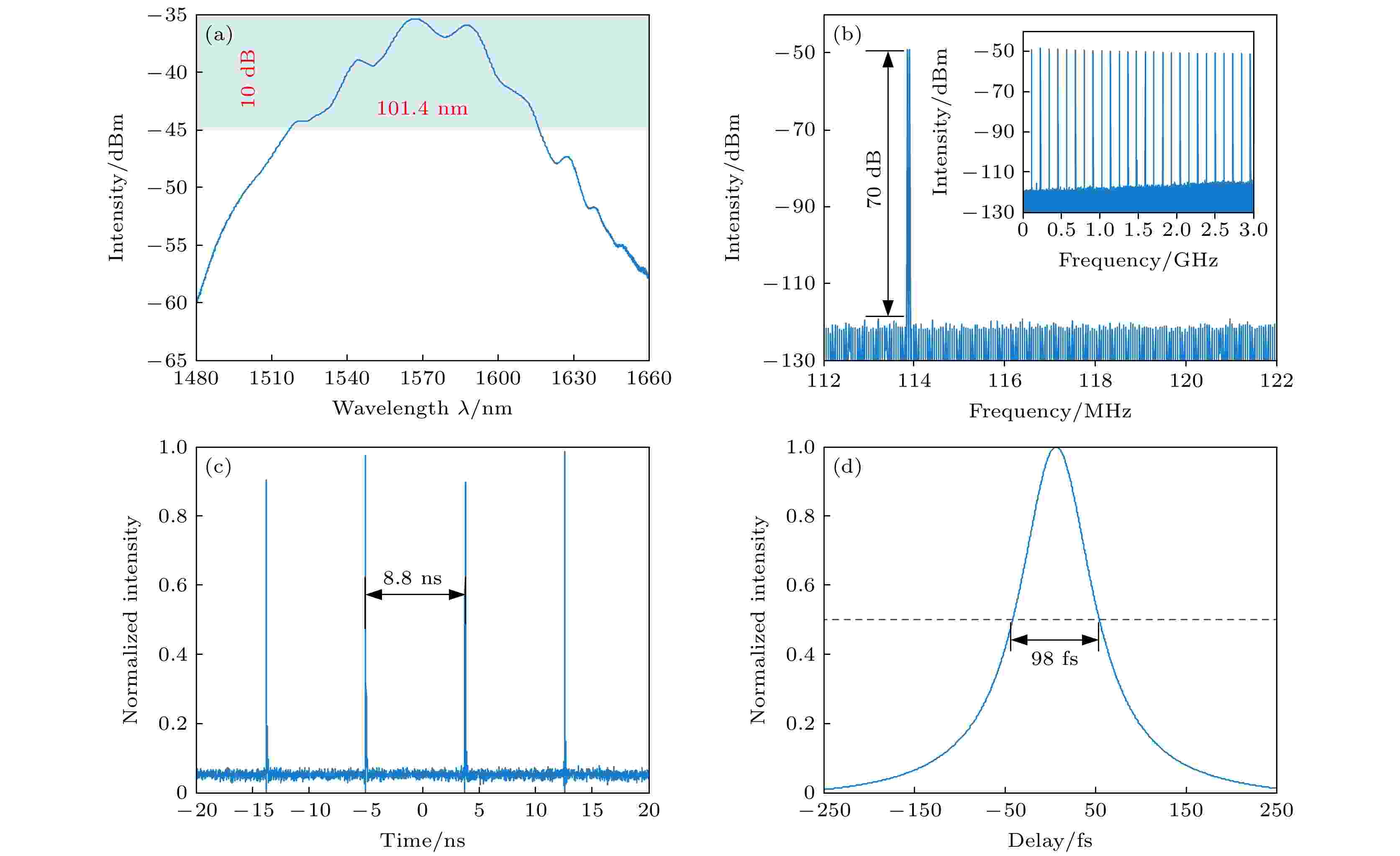
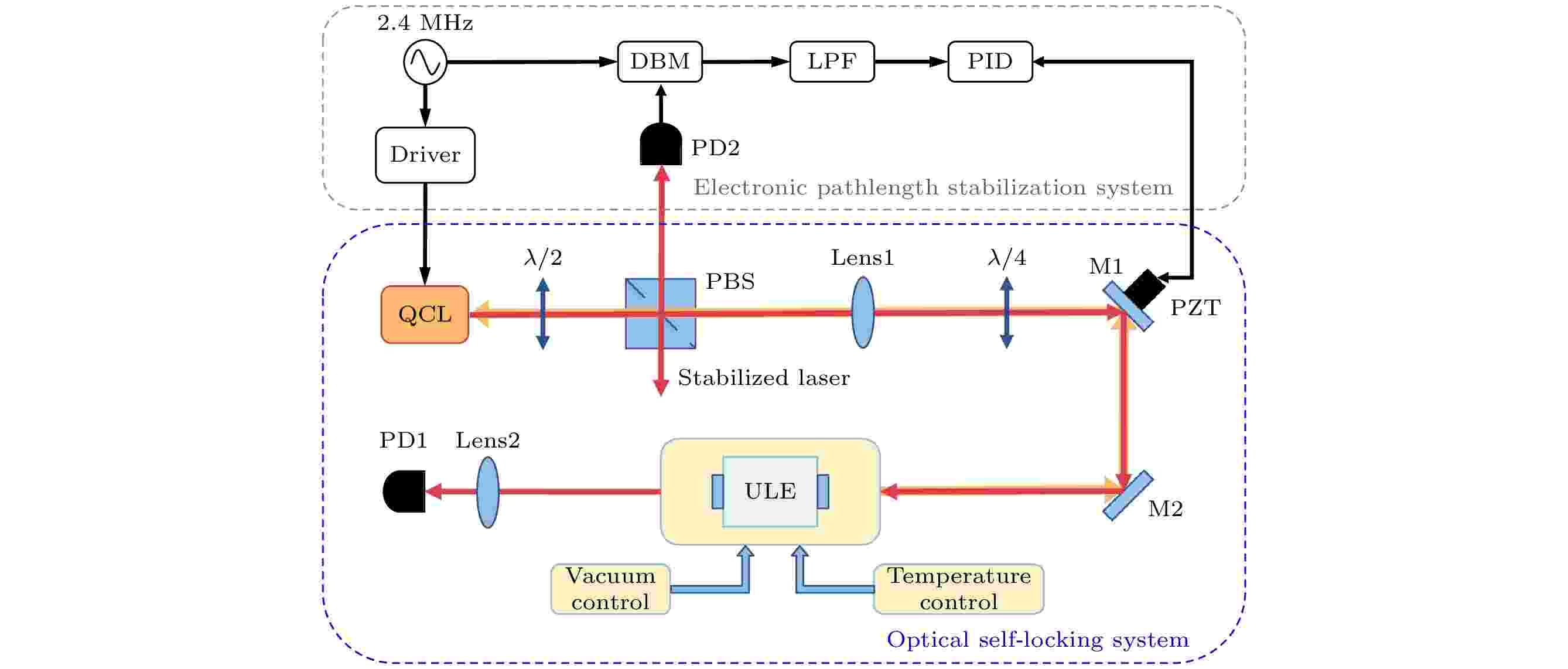
Mid-infrared precision spectroscopy has important applications in the fields of trace gas detection and the determination of fundamental physical constants. However, due to the limited commercialization of related technologies, there is a lack of narrow linewidth laser sources or linewidth narrowing approaches in the mid-infrared region, as well as stable mid-infrared frequency standards. The most commercialized and widely used mid-infrared laser source is the quantum cascade laser (QCL). But its free-running linewidth is more than MHz scale due to the influence of laser drive current noise and temperature fluctuation. This impedes the development of precision spectroscopy in this region. In this work, we introduce a technique for generating a narrow linewidth, stable mid-infrared laser by using optical feedback frequency locking, with a high-finesse mid-infrared ultrastable Fabry-Pérot cavity as the frequency reference. The optical cavity consists of two high reflectivity mirrors separated by ultra-low expansion (ULE) material with a low temperature expansion coefficient, and its temperature is precisely controlled. And the cavity is also surrounded in a vaccum cavity made of stainless steel. All these measures ensure the cavity length and its longitudinal mode stability. By using optical feecback, a QCL is locked to the cavity, which stabilizes the laser frequency and narrows the laser linewidth. In order to improve the long-term stability of the optical feedback, an active servo is leveraged to control the feedback phase. The error signal for the servo is obtained by using the method similar to the Pound-Derver-Hall locking. In this work, we first theoretically analyze the feasibility of laser to F-P cavity frequency locking by optical feedback. We propose the laser frequency response model with a linear F-P cavity under optical feedback, and analyze the influence of the direct cavity reflection on the laser frequency. Then the experimental demonstration is conducted. Firstly, we measure the reflectivity of the cavity mirror by using cavity ring-down spectroscopy, resulting in a cavity finesse of 30200 and a cavity mode linewidth of 49.7 kHz. After that, we successfully achieve optical feedback frequency locking, and consecutive cavity transmission is observed. The error signal for the control of the optical feedback phase is used to evaluate the locking performance by converting it into the laser frequency noise. By analyzing the noise spectral density, the QCL linewidth is narrowed to 0.3 Hz on a short timescale (< 10 ms). And the long-term stability is suspected to be dedicated by the temperature variation of the optical cavity, resulting in a laser frequency drift 20 kHz/12 h. The narrow linewidth stabilized mid-infrared laser source obtained with this technique is expected to serve as an effective frequency reference source for mid-infrared precision spectroscopic measurements.

2024, 73 (1): 014206.
doi: 10.7498/aps.73.20231272
Abstract +
The stimulated Brillouin scattering (SBS) effect has the advantages of narrow spectral line width, frequency stability, and sensitivity to gain direction, which is commonly used in the field of integrated photonic devices, such as lasers, slow light generation and microwave photonic filters. In practical applications, due to the low gain coefficient of SBS in traditional chalcogenide waveguides, there are high threshold of pumping power and long waveguide length. In this work, an inverted-ridge waveguide structure with air slot is designed by adopting As2S3 and SiO2, which presents high backward stimulated Brillouin scattering (BSBS) gain coefficient. This chalcogenide inverted-ridge optical waveguide with air slot can better confine the optical field and acoustic field within the ridge region for improving the coupling efficiency between optical field and acoustic field. More significantly, adding an air slot into the ridge region of this chalcogenide waveguide will produce powerful radiation pressure at the boundary between the air slot and As2S3. Owing to the fact that the acoustic field is mainly distributed near the air slot in the ridge region, the coupling effect of the radiation pressure and acoustic field is significantly enhanced, leading to a significant increase in BSBS gain coefficient. In this work, the optical fundamental mode as optical mode due to the chalcogenide waveguide with submicron size structure and the six lowest order acoustic modes that meet the matching vector conditions as acoustic mode are calculated, and it is found that the fifth order acoustic mode achieves a maximum BSBS gain coefficient in the six acoustic modes. On this basis, by scanning the waveguide structural parameters of the air slot width, waveguide ridge width and height, and waveguide thickness, the BSBS gain coefficient is as high as 8.22×10⁴ W–1·m–1, which is more than three times the currently reported chalcogenide waveguide with non-suspended structure. Additionally, the calculation results also indicate that this chalcogenide waveguide with a smaller effective mode field area has a higher BSBS gain coefficient in the same optical mode and acoustic mode, providing a new idea for further improving the BSBS gain coefficient in the design of waveguide structure. At the same time, the influence of optical loss on BSBS gain is also analyzed, and it is found that when the waveguide length exceeds the optimal value, the lost energy caused by the optical loss will be beyond the input energy of the pump optical wave, causing the power of the stokes optical wave to begin to decrease. However, the improvement of the power of pump optical wave not only increases the maximum power of the Stokes optical wave, but also raises the optimal value of the waveguide length. The results of simulation calculation show that when the input power of pump optical wave is about 20 mW, this chalcogenide waveguide with only 2 cm waveguide length has a BSBS gain of 100 dB, which has the advantages of low pumping power and short waveguide length in the currently reported on-chip integration of chalcogenide waveguides.

2024, 73 (1): 014207.
doi: 10.7498/aps.73.20231291
Abstract +
In this paper, based on the research of zoom liquid lens with parallel plate electrode and the principle of dielectrophoresis, a model of the biconvex liquid lens with circular hole plate electrode structure is proposed, which is a novel three-layer liquid lens structure. The dielectrophoretic effect refers to the phenomenon that free dielectric molecules will be polarized and moved by the force in a non-uniform electric field, thus deforming the dielectric liquid. In the dielectrophoretic liquid lens, only two insulating liquid materials with large refractive index difference and dielectric constant difference need to be selected, which can increase the selection range of liquid materials. The liquid lens structure mainly consists of a piece of double-sided conductive flat plate ITO glass with a circular hole and two pieces of single-sided conductive flat plate ITO glass, which respectively form two sets of flat electrode structures to control the upper interface and lower interface of the liquid droplet. In this structure, the influences of the intermediate glass plate on the focus and imaging are reduced by using the flat plate electrode with circular hole. The theoretical analysis of the structure is carried out with simulation software. Firstly, the models of the biconvex liquid lens with circular hole plate electrode under different voltages are built with Comsol software, the data of upper interface and lower interface of the liquid droplet are exported. Then by using Matlab, the surface shapes of the upper interface and lower interface of the droplet are fitted and the corresponding aspheric coefficients are obtained. Finally, the optical models are built with Zemax software, the imaging optical paths and the variation range of focal length under different voltages are analyzed. On the basis of the simulation, the corresponding device is made, and the specific experimental analysis is carried out. The surface patterns of the upper interface and lower interfaces of the droplet of the biconvex liquid lens under different voltages are recorded, the focal length and imaging resolution of the liquid lens are measured. When the operating voltage is in a range of 0–260 V, the focal length varies from 23.8–17.5 mm, which is basically consistent with the simulation results (22.6–15.9 mm). The feasibility of the structure of the biconvex liquid lens with circular hole plate electrode structure is verified experimentally. The imaging resolution can reach 45.255 lp/mm. The results show that this proposed novel three-layer liquid structure of the biconvex liquid lens has the characteristics of simple structure, easy-to-realize and good imaging quality. Therefore, the research of this biconvex liquid lens can provide a new idea for expanding the high-resolution imaging research of liquid lenses and their applications.

2024, 73 (1): 014208.
doi: 10.7498/aps.73.20231155
Abstract +
In aerospace, petrochemical, gas turbines and other high-temperature environments, pressure measurement of equipment has always been a challenge to be solved. The electrical high temperature pressure sensor has the problem of component failure in high temperature environment, and it is difficult to use in the high temperature environment for a long time. The detection device of the optical fiber sensor does not include electrical components, so it has the advantages of high working temperature, high measurement accuracy, anti-electromagnetic interference and so on. In order to use a sensor to measure pressure in high temperature environment, a temperature-weakly sensitive optical fiber micro-electro-mechanical system (MEMS) pressure sensing technology is proposed. The technique uses extrisic Fabry-Pérot interference (EFPI) model. It uses the MEMS pressure chip to passively modulate the optical signal of the interference, and then realizes the pressure signal measurement. Among them, MEMS pressure sensitive chip is the core component of the sensor. The MEMS pressure sensitive chip adopts the design method of all solid state vacuum absolute pressure. Change in environmental pressure will deform the membrane. This phenomenon can cause change in the cavity of the EFPI cavity. Therefore, stress information can be obtained by measuring changes in EFPI cavity. The thermal stress and temperature parasitical response introduced by thermal expansion of the material are calculated by simulation. The influence of temperature signal on chip displacement is analyzed by the above results. On this basis, a prototype of high temperature pressure sensor is developed by combining the sub-micron white light interference response technology and low thermal stress packaging technology. In order to test the ability of the sensor to implement actual measurement, this paper carry out the pressure test and high temperature test respectively. When the pressure changes from 0 kPa to 100 kPa, the spectral intensity of the sensor output has a linear relationship with the pressure. During the temperature changing from 20–400 ℃, the spectral intensity of the sensor output does not change significantly. The experimental test results show that the pressure measurement of 0–100 kPa can be satisfied in the range of 20–400 ℃, and the measurement error introduced by temperature change is less than 4%. Therefore, the fiber pressure sensor can be used to measure the pressure in high temperature environment.
PHYSICS OF GASES, PLASMAS, AND ELECTRIC DISCHARGES

2024, 73 (1): 015101.
doi: 10.7498/aps.73.20230712
Abstract +
In this paper, the effect of pre-ionization on the small-gap and large-gap direct-current glow discharge at atmospheric pressure are investigated based on a two-dimensional self-consistent fluid model. For both the discharges, the results show that with the enhancement of pre-ionization, the charged particle distribution gradually shifts toward the cathode along the discharge direction, making the cathode fall zone shrink continuously. The width of the positive column region, negative glow space, and cathode fall zone continuously extend along the vertical discharge direction, and the distribution of electron density and ion density are more uniform. For the electric field, with the enhancement of pre-ionization, the longitudinalal component distribution of the electric field in the cathode fall zone gradually contracts toward the cathode, and the overall electric field near the cathode decreases and becomes more uniformly distributed. The transverse component distribution of the electric field gradually decreases and shrinks toward the wall. The overall electron temperature in the discharge space decreases with the enhancement of the pre-ionization level, and the electron temperature distribution in the cathode fall zone gradually shrinks toward the cathode. In addition, the overall potential of the discharge space also decreases. The introduction of pre-ionization significantly reduces the maintaining voltage and discharge power of the direct-current glow discharge. Furthermore, the potential drop in the small-gap discharge is always concentrated in the cathode fall zone as the pre-ionization increases, while the potential drop in the large-gap discharge is gradually shifted from the cathode fall zone to the positive column region. This simulation shows that the pre-ionization not only effectively enhances the discharge uniformity, but also largely reduces the maintaining voltage and energy consumption of the direct-current glow discharge. This work is an important guideline for further optimizing the electrode configuration and the operating parameters of the plasma source.

EDITOR'S SUGGESTION
2024, 73 (1): 015201.
doi: 10.7498/aps.73.20231216
Abstract +
Warm dense matter (WDM), a state of matter that lies at the frontier between condensed matter and plasma, is one of the main research objects of high energy density physics (HEDP). Comparing with the isolated atom, the electron structure of WDM will change because of the influence of density and temperature effect. Both the accurate theoretical representation and the accurate experimental study of WDM electron structure are challenging, as it is strongly coupled and partially degenerated. In this work, an experimental method of studying the ionization distribution of WDM based on X-ray fluorescence spectroscopy is developed. In the experiment, in a specially designed hohlraum, warm and dense titanium with several tens of electron volts and nearly solid density is produced by simultaneous driving of high-energy X-ray heating and shock compression. Then, using the characteristic line spectrum emitted by the laser irradiation on pump material (Vanadium) as a pump source, the titanium emits fluorescence. The X-ray fluorescence spectra of titanium with different states (cold sample, 1.8–4.5 g/cm3 and 1–25 eV) are diagnosed by changing the experimental strategy. The experimental results indicate that the line profiles of Kα and Kβ fluorescence spectrum of the heated sample change obviously compared with those of the cold sample. According to the theoretical calculation of the two-step Hartree-Fock-Slater (TSHFS) method, the main reason for the change of the line profile is the change of ionization distribution caused by temperature rising. The future work will focus on optimizing the experimental method of X-ray fluorescence spectrum, such as improving the spectrum resolution, characterizing the temperature and density experimentally, obtaining a set of ionization distribution data, and then studying the influence of dense environment on electronic structure.
2024, 73 (1): 015202.
doi: 10.7498/aps.73.20231283
Abstract +
Compared with two-electrode gas spark switch, three-electrode gas spark switch has the advantages of lower operating voltage, higher reliability and less discharge jitter, so it has been widely used in pulse power systems. However, due to the characteristics of pulse power technology, the gas spark switch is easy to cause ablation on the electrode surface during use, and the metal particles generated by ablation will significantly affect the stability and reliability of the switch. In this work the discharge process of the three-electrode gas spark switch under atmospheric pressure nitrogen environment is simulated first. In this model, the ionization coefficient near the trigger electrode is modified to compensate for the shortcomings of the local field approximation, and the relevant mathematical derivation process is given. The formation of the initial electrons is described by the field electron emission phenomenon, and the development process of electron collapse into the streamer is obtained. The physical mechanism of switch on is investigated, and the development process of each stage of switch discharge is described in detail. Then, the discharge process of the switch is studied when there are metal particles near the trigger. The study shows that the presence of metal particles enhances the electric field near the trigger and accelerates the formation of the initial electron cloud. In addition, in the presence of metal particles, the metal particles and the trigger will first break down, forming a high-density plasma channel after the breakdown, and becoming the source of the subsequent flow development. At the same time, because the metal particles on the channel have an obstructing effect on the streamer development, the streamer generates a discharge branch after contacting metal particles. In the end, the influences of metal particles of different shapes and sizes on the discharge process are discussed. The results show that metal particles with sharp shapes have stronger electric field distortion, when the electric field intensity is large enough, it may cause field emission on the surface of metal particle. And it is also made clear that the size of metal particle is small, the obstruction of the development path of streamer is small, and the streamers quickly converge behind the particles.

2024, 73 (1): 015203.
doi: 10.7498/aps.73.20231158
Abstract +
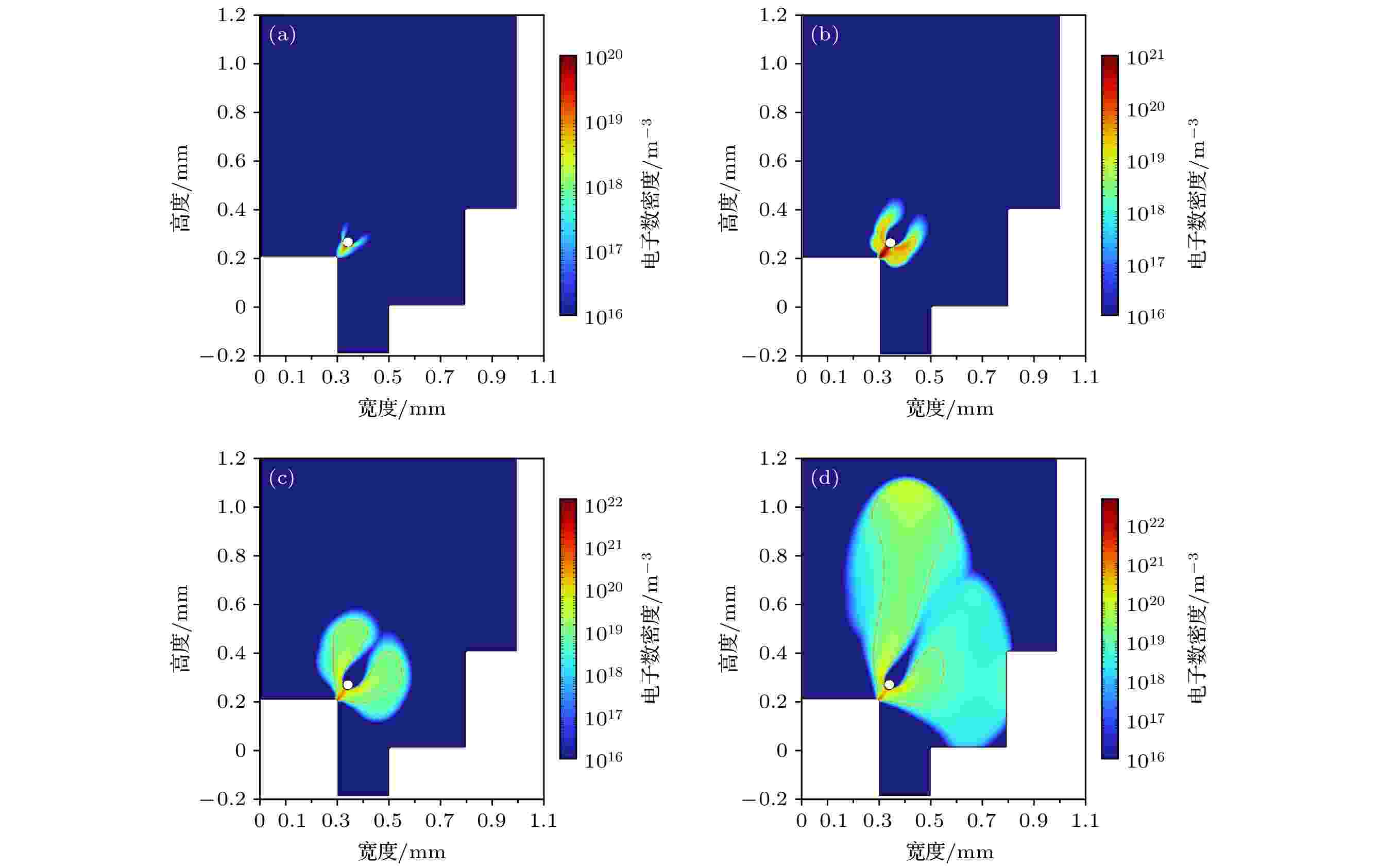
Extreme ultraviolet (EUV) light source is an important part of EUV lithography system in semiconductor manufacturing. The EUV light source requires that the 4p64dn-4p54dn+1 + 4dn–14f transitions of Sn8+~13+ ions emit thousands of lines which form unresolved transition arrays near 13.5 nm. Laser-induced discharge plasma is one of the important technical means to excite target into an appropriate plasma condition. Laser-induced discharge plasma has a simple structure and a low cost. It also has important applications in mask inspection, microscopic imaging, and spectral metrology. In the design and production process, there are many factors that can influence the conversion efficiency, such as current, electrode shape, and laser power density. The simulation method is a convenient way to provide guidance for optimizing the parameters. In this paper, a completed radiation magneto-hydrodynamic model is used to explore the dynamic characteristics of laser-induced discharge plasma and its EUV radiation characteristics. To improve the accuracy, a more detailed global equation of state model, an atomic structure calculation model including relativistic effect and a collision radiation model are proposed simultaneously. The simulation reconstructs the discharge process effectively, which is divided into five stages in the first half cycle of current, including expansion of laser plasma, column formation of discharge plasma, diffusion of discharge plasma, contraction of discharge plasma, and re-diffusion of discharge plasma. It is revealed that the pinch effect during the current rising time exerts a significant influence on the generation of EUV radiation. The conversion efficiency of EUV radiation is still low under our existing conditions, and hopefully a higher rising rate of current can improve the conversion efficiency in the future work.
CONDENSED MATTER: STRUCTURAL, MECHANICAL, AND THERMAL PROPERTIES

2024, 73 (1): 016301.
doi: 10.7498/aps.73.20231279
Abstract +
Hittorf’s violet phosphorene is a novel two-dimensional material with stable structure and excellent optoelectronic properties. Studying the doping effect helps to understand its physical essence and is of great significance in further developing nanoelectronic devices. In this paper, the first-principles method based on density functional theory is used to study the electromagnetic properties of the non-metallic element B-, C-, N-, and O-doped single-layer violet phosphene. The results show that there is no magnetism after having doped boron and nitrogen, and the system still behaves as a nonmagnetic semiconductor, while carbon doping and oxygen doping cause spin splitting, and the violet phosphorene transforms from a nonmagnetic semiconductor to a bipolar magnetic semiconductor, and its spin density is mainly distributed in the P atom and gap region, rather than on the impurity. The direction of spin polarization of its carrier can be reversed by adjusting the electric field of O-doped violet phosphorene. When a certain size of forward or reverse electrostatic field is applied, the band dispersion becomes stronger, and the O-doped violet phosphorene transforms into a half-metallic magnet with 100% downward or upward spin polarization at the Fermi level. The field effect spin filter based on O-doped violet phosphorene can reverse the direction of spin-polarized current by changing the direction of the gate voltage. This study shows that O-doped violet phosphorene is expected to be an ideal candidate material for two-dimensional spin field-effect transistors, bipolar magnetic spintronic devices, dual channel field effect spin filters, and field-effect spin valves.

2024, 73 (1): 016801.
doi: 10.7498/aps.73.20231296
Abstract +
Thin liquid film near the gas-liquid-solid three phase contact line is the core area of oil and gas production, phase-change heat transfer, and material synthesis systems. Although there are many experimental studies on fluid dynamics in the contact line region, the prediction of contact angle is still difficult, and the bottleneck lies in the special structure of thin liquid film in the contact line region. Because the microstructure of thin liquid film is not well understood, the prediction of dynamic contact angle is always controversial. At present, the main controversial points focus on whether the microscopic contact angle changes with speed, and whether the microscopic contact angle is the same as the macroscopic contact angle. Therefore, it is crucial to monitor the dynamic process of the microscopic contact angle in the thin liquid film region of the contact line. In this work, the wetting system of 50 nm liquid droplets on different solid surfaces is constructed by molecular dynamics simulation, and the structure and migration mechanism of thin liquid film are studied. The structure of the precursor liquid film in the completely wetting droplet advancing contact line region and the nanoscale convex structure in the partially wetting droplet advancing contact line region are obtained. The precursor liquid film is 2–3 molecular layers in thickness, leading the droplet to move forward. However, there is no precursor liquid film in a partially wetting system, and the convex nano-bending larger than 10 nm is formed in the wetting process, resulting in the microscopic contact angle. By comparing the difference between the absolute smooth surface dynamic wetting process and the actual solid surface dynamic wetting process, the dynamic evolution law of the micro contact angle and the macro contact angle with time are obtained for the first time in the simulation. The liquid molecules in the contact line region are tracked and statistically analyzed by means of particle tracer. It is revealed that the liquid molecules in thin liquid film change from sliding mode to rolling mode with speed increasing under the action of solid surface friction, and then the air entrainment at the bottom of the contact line leads to slip and sputtering. The research results are expected to provide theoretical guidance for the following three directions: 1) improving heat transfer efficiency of micro and nano device based on wettability control; 2) improving the imbibition displacement efficiency of shale oil micro-nano matrix based on wettability regulation; 3) constructing universal contact angle prediction model.
CONDENSED MATTER: ELECTRONIC STRUCTURE, ELECTRICAL, MAGNETIC, AND OPTICAL PROPERTIES
2024, 73 (1): 017101.
doi: 10.7498/aps.73.20231252
Abstract +
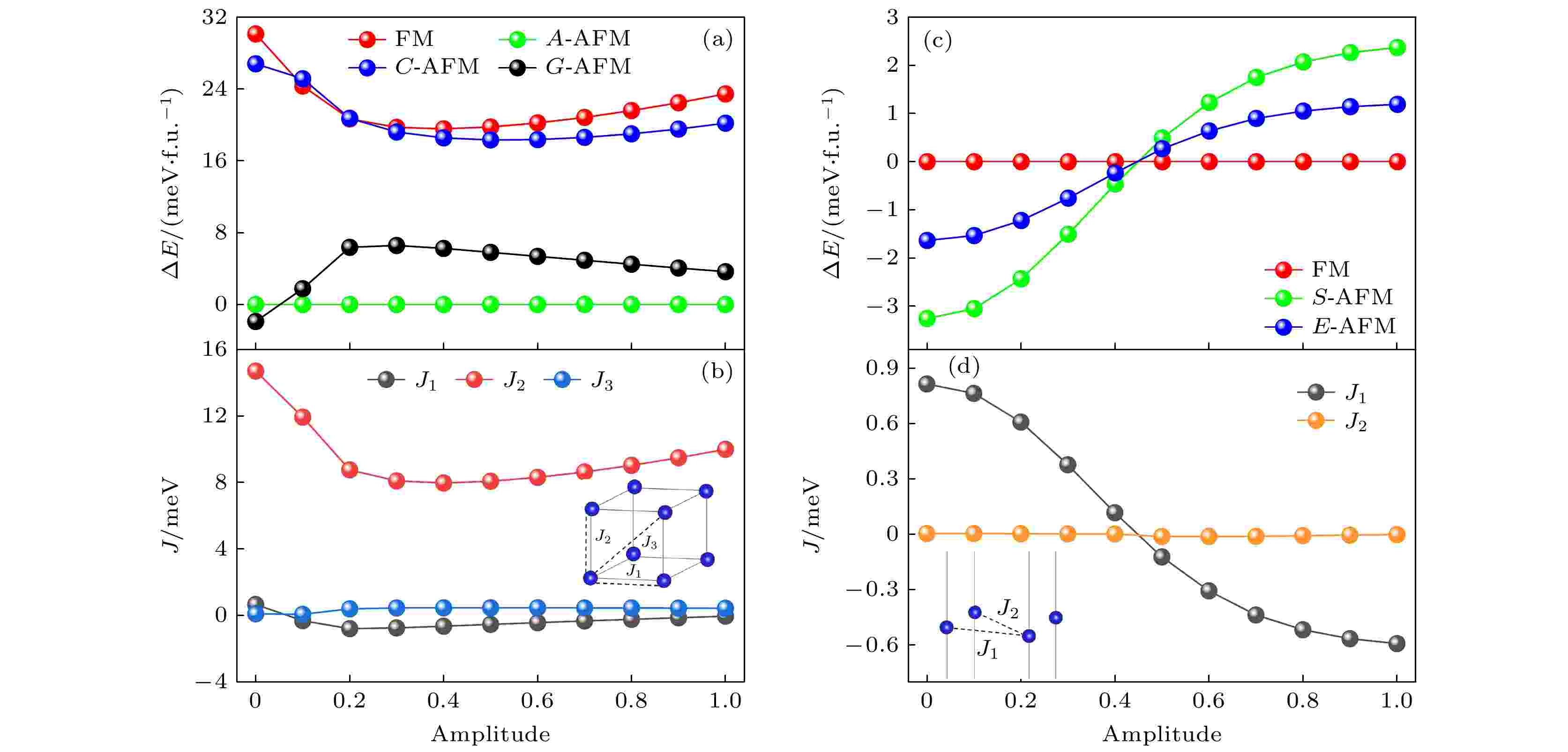
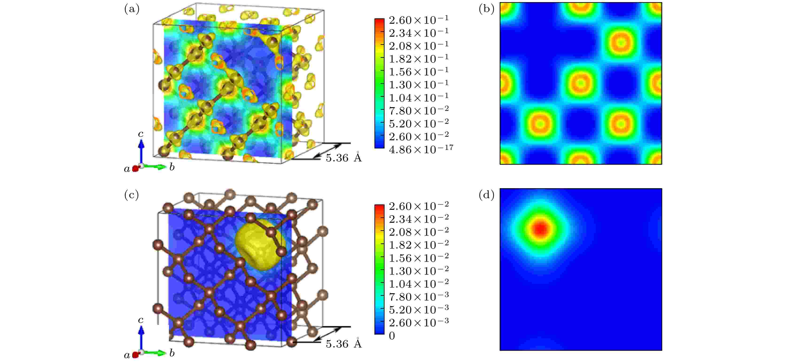
With the decrease of system dimension, the quantum confinement effect and electronic correlation interaction inside the material will be enhanced correspondingly, often resulting in some novel physical properties. Recently, the freestanding perovskite oxide films as low as the monolayer limit have been successfully prepared and can be transferred to any desired substrate, which provides a great opportunity for exploring the functional properties of two-dimensional perovskite. In perovskite materials, Jahn-Teller distortion and orbital order often cause a variety of correlated electronic behaviors. However, unlike van der Waals materials that retain their structural and chemical bonding characteristics when they are reduced to the monolayer limit, perovskite materials may undergo structural reconstruction when they are reduced to two dimensional structures. Therefore, what are the issues to be solved urgently are whether Jahn-Teller distortion and related effects exist in the perovskite monolayer limit, and whether two-dimensional perovskite can exhibit some new properties different from its bulk phase. In this work, perovskite fluoride KCuF3 and its monolayer have been comparatively studied by the first-principles calculation, symmetry analysis, and Monte Carlo simulation methods, revealing the change in lattice dynamics, structural, electronic, and magnetic properties caused by dimensionality reduction in perovskites. The results show that the cooperative Jahn-Teller distortion and the in-plane staggered orbital order occurring in the KCuF3 bulk can be retained to the monolayer limit. However, unlike the bulk phase, the Jahn-Teller distortion mode appears as a soft mode of the prototype phase in the monolayer, and the insulating property of the monolayer does not rely on the emergence of the Jahn-Teller distortion, but it is related to the enhancement of the electronic correlation effect. The staggered orbital order causes the nearest-neighbor exchange interaction to be ferromagnetic, resulting in the monolayer being a two-dimensional ferromagnetic insulator, different from the antiferromagnetic phase in the bulk. Monte Carlo simulations predict that the Curie temperature of the monolayer is about 5 K, which is much lower than the Néel temperature of the bulk phase, indicating that the disappearance of interlayer coupling leads to a significant reduction in the magnetic phase transition temperature. This work provides guidance and reference for studying the two-dimensional perovskite materials and designing the perovskite-based two-dimensional ferromagnets.

2024, 73 (1): 017102.
doi: 10.7498/aps.73.20231147
Abstract +
In this work, the formation energy, band structure, state density, differential charge density and optoelectronic properties of undoped β-Ga2O3 and Si doped β-Ga2O3 are calculated by using GGA+U method based on density functional theory. The results show that the Si-substituted tetrahedron Ga(1) is more easily synthesized experimentally, and the obtained β-Ga2O3 band gap and Ga-3d state peak are in good agreement with the experimental results, and the effective doping is more likely to be obtained under oxygen-poor conditions. After Si doping, the total energy band moves toward the low-energy end, and Fermi level enters the conduction band, showing n-type conductive characteristic. The Si-3s orbital electrons occupy the bottom of the conduction band, the degree of electronic occupancy is strengthened, and the conductivity is improved. The results from dielectric function ε2(ω) show that with the increase of Si doping concentration, the ability to stimulate conductive electrons first increases and then decreases, which is in good agreement with the quantitative analysis results of conductivity. The optical band gap increases and the absorption band edge rises slowly with the increase of Si doping concentration. The results of absorption spectra show that Si-doped β-Ga2O3 has the ability to realize the strong deep ultraviolet photoelectric detection. The calculated results provide a theoretical reference for further implementing the experimental investigation and the optimization innovation of Si-doped β-Ga2O3 and relative device design.

EDITOR'S SUGGESTION
2024, 73 (1): 017801.
doi: 10.7498/aps.73.20231322
Abstract +
TmFeO3 exhibits rich physical properties such as magneto-optical effect, multiferroicity, and spin reorientation, making it possess significant research value in condensed matter physics and materials science. In this study, we utilize a time-domain terahertz magneto-optical spectroscopy system to investigate the changes in spin resonance frequency of TmFeO3 single crystal at T = 1.6 K under external magnetic fields in a range of 0–7 T. The TmFeO3 sample is grown in an optical floating zone furnace and its crystallographic orientation is determined by using back-reflection Laue X-ray photography with a tungsten target. The measurement setup is a self-built time-domain terahertz magneto-optical spectroscopy system, with magnetic fields in a range of 0–7 T, temperatures in a range of 1.6–300 K, and a spectral range of 0.2–2.0 THz. A pair of 1 mm-thick ZnTe nonlinear crystals is used to generate and detect terahertz signals through optical rectification and electro-optic sampling technique. The system variable temperature and magnetic field are controlled by a superconducting magnet. In experiments, a linearly polarized terahertz wave is vertically incident on the sample surface, and its magnetic component HTHz is parallel to the sample surface. By rotating the sample, the angle (θ) between macroscopic magnetic moment M and HTHz can be tuned, achieving selective excitations of the two modes, that is, θ = 0 for q-AFM mode and 90° for q-FM mode. Terahertz absorption spectrum results indicate that as the magnetic field increases, the quasi-ferromagnetic resonance (q-FM) of TmFeO3 single crystal shifts towards high frequencies, and quasi-antiferromagnetic resonance (q-AFM) transits to q-FM under low critical magnetic fields (2.2–3.6 T). Through magnetic structure analysis and theoretical fitting, it is confirmed that the magnetic moment of the single crystal undergoes magnetic field induced spin reorientation. This study is helpful in better understanding of the regulation mechanism of the internal magnetic structure of rare earth ferrite under the combined action of external magnetic field and temperature field, and also in developing related spin electronic devices.
2024, 73 (1): 017802.
doi: 10.7498/aps.73.20231269
Abstract +
Metal-matrix diamond composites have been extensively used and studied, but vacancies, doping, and other defects caused by the pretreatment of the diamond surface significantly affect the interface property between the metal base and diamond. Although techniques like transmission electron microscopy and spectroscopy analysis have been used to detect defects, they present certain limitations. Calculating the positron annihilation lifetime in diamond provides an accurate assessment of interface defect in the diamond. This study uses first-principles calculation methods and adopts various positron annihilation algorithms and enhancement factors, to compute the positron annihilation lifetimes in ideal diamond crystals, single vacancies, and diamond crystals doped with B, Cr, Mo, Ti, W, and Zr. The results, obtained by using local density functional in combination with Boronski & Nieminen algorithms and random-phase approximation restriction as annihilation enhancement factors, indicate that the computed positron annihilation lifetime of diamond is 119.87 ps, which is consistent closely with the experimental result in the literature. Furthermore, after B, Cr, Mo, Ti, W, and Zr atoms are doped into diamond (doping atomic concentration of 1.6%), the positron annihilation lifetimes change from a single vacancy 119.87 ps to 148.57, 156.82, 119.05, 116.5, 117.62, and 115.74 ps respectively. This implies that the defects due to doped atoms in diamond change their positron annihilation lifetimes, with the influence varying according to the different atoms doped. Based on the calculated electron density in diamond vacancies and doped atom areas, it is discovered that doping atoms do not cause severe distortion in the diamond lattice. However, after B and Cr atoms are doped, the positron annihilation lifetime increases significantly. The primary reason is that the relatively low positron affinity of B and Cr atoms results in an extended positron residence time in the vacancy, thereby increasing the annihilation lifetime. Overall, vacancies and doped atom defects in diamond will cause its positron annihilation lifetime to change. The above conclusions provide crucial theoretical references for detecting and identifying interface defects caused by doping treatment on the diamond surface during the preparation of metal-matrix diamond composites.
GEOPHYSICS, ASTRONOMY, AND ASTROPHYSICS

EDITOR'S SUGGESTION
2024, 73 (1): 019101.
doi: 10.7498/aps.73.20231087
Abstract +
Owing to the need for a hydrostatic high-pressure cubic large cavity (hexahedral top) press used in high-pressure research and production of superhard material, two kinds of pyrophyllite powder compacts (A and B) from pyrophyllite mine in South Africa are prepared, and compared with the domestic yellow pyrophyllite powder compacts (Mentougou, Beijing) produced by the same process, to establish experimental methods and physical criteria for evaluating the pressure transmission and sealing performance of pyrophyllite. During the experiment, standard pressure materials such as Bi, Tl, and Ba are used to in-situ calibrate the pressure at the central positions and sealing edges of the pyrophyllite pressure chambers from the three aforementioned compacts under normal pressure conditions. Additionally, the silver melting point method is employed to obtain the corresponding relationship between chamber pressure at high temperature and system loading when using these three types of pyrophyllite as load-transmitting sealing materials. The results show that under the same hydraulic pressure loading, the difference in pressure at the central position between South African pyrophyllite B powder blocks and domestically produced pyrophyllite powder blocks does not exceed 0.1 GPa. Furthermore, in pressurization process and depressurization processe, the differences in pressure between the central position and the sealing edge of the pyrophyllite blocks are notably similar. Compared with South African pyrophyllite A powder blocks, pyrophyllite B powder blocks exhibit a closer resemblance to domestically produced pyrophyllite powder blocks in terms of high-temperature load transmission and sealing performance. Pyrophyllite B powder blocks from South Africa have the potential to serve as a substitute for domestically produced pyrophyllite without changing the existing superhard material synthesis process, making them promising candidates for use as load-transmitting media and sealing materials. These research findings hold significant academic importance in the realms of high-pressure research and superhard material production. They provide valuable insights into the selection of suitable transmission and sealing materials and the optimization of high-pressure experimental conditions. Additionally, this study presents robust method and criteria for experimental procedures and performance assessment.
