-
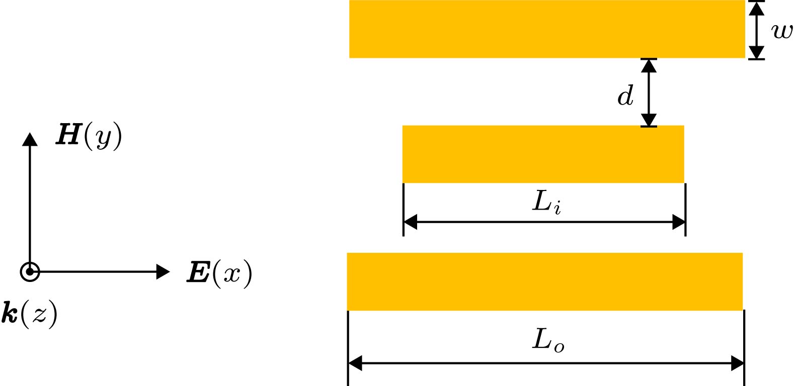
A symmetrical gold nanorod trimer structure consisting of a short center nanorod and two long nanorods on both sides is proposed. The scattering spectra, electromagnetic field and current density vector distributions across the central cross section of the nanorod trimer are calculated by the finite difference time domain method, and the effects of structural parameters and dielectric environment on Fano resonance characteristics are theoretically investigated in detail. The results show that the Fano resonance can be generated mainly due to the interference between the bonding electric dipole mode in lower energy and the antibonding electric dipole mode or antiphase magnetic dipole mode in higher energy. The Fano dip is blue-shifted with the decrease in the short nanorod length, the size of whole trimer structure with constant displacement, or the refractive index of dielectric medium in the gaps between the central nanorod and two side nanorods; the resonance intensity on both sides of the Fano dip also changes. Meanwhile, the bonding mode on the red side of the Fano dip is gradually dominated by the electric dipole mode of two side nanorods, and the spectral intensity increases, while the antibonding mode on the blue side gradually evolves into the short nanorod-dominated antiphase magnetic dipole mode, and the spectral intensity becomes weaker. The increase in the inter-rod spacing also leads the Fano dip to be blue-shifted, and a similar change in the spectral intensity occurs on both sides of the Fano dip, due to the degeneration of bonding and antibonding modes caused by the decrease of near-field coupling between the short nanorod and two side nanorods, which finally degenerate into the electric dipole modes generated by the short nanorod or the two side nanorods, respectively. In addition, the Fano dip is insensitive to the change of the side nanorod length, but the relative resonance intensity on both sides of the Fano dip also changes. Furthermore, it is found that the spectral contrast ratio of the Fano resonance first increases and then decreases by varying the above-mentioned structural parameters or dielectric environment. These results are expected to be used for guiding the design of Fano controllable nanostructures and also for developing the applications of specific micro-nano photonics.
-
Keywords:
- Fano resonance /
- surface plasmon polariton /
- nanorod /
- finite difference time domain
[1] Zhang S P, Xu H X 2016 Nanoscale 8 13722
 Google Scholar
[2] Biswas S, Duan J, Nepal D, Park K, Pachter R, Vaia R A 2013 Nano Lett. 13 6287
 Google Scholar
[3] Artar A, Yanik A A, Altug H 2011 Nano Lett. 11 3694
 Google Scholar
[4] Wu D, Liu C, Liu Y, Yu L, Yu Z, Chen L, Ma R, Ye H 2017 Opt. Lett. 42 450
 Google Scholar
[5] Zhang J, Chen S, Wang J,Mu K, Fan C, Liang E, Ding P 2018 Sci. Rep. 8 740
 Google Scholar
[6] Limonov M F, Rybin M V, Poddubny A N, Kivshar Y S 2017 Nat. Photon. 11 543
 Google Scholar
[7] Chen J, Gan F, Wang Y, Li G 2018 Adv. Opt. Mater. 6 1701152
 Google Scholar
[8] Huang C Y, Chang H C 2019 IEEE Photon. J. 11 4800208
 Google Scholar
[9] Li G Z, Hu H J, Wu L 2019 Phys. Chem. Chem. Phys. 21 7654
 Google Scholar
[10] Wu C, Khanikaev A B, Shvets G 2011 Phys. Rev. Lett. 106 107403
 Google Scholar
[11] Chang W S, Lassiter J B, Swanglap P, Sobhani H, Khatua S, Nordlander P, Halas N J, Link S 2012 Nano Lett. 12 4977
 Google Scholar
[12] Yu Y, Xue W, Semenova E, Yvind K, Mork J 2017 Nat. Photon. 11 81
 Google Scholar
[13] Hu H J, Zhang F W, Li G Z, Chen J Y, Li Q, Wu L J 2018 Photon. Res. 6 204
 Google Scholar
[14] Yang Z J, Hao Z H, Lin H Q, Wang Q Q 2014 Nanoscale 6 4985
 Google Scholar
[15] 黄运欢, 李璞 2015 物理学报 64 207301
 Google Scholar
Huang Y H, Li P 2015 Acta Phys. Sin. 64 207301
 Google Scholar
[16] Zhang Y, Jia T Q, Zhang H M, Xu Z Z 2012 Opt. Lett. 37 4919
 Google Scholar
[17] Fu Y H, Zhang J B, Yu Y F, Lukyanchuk B 2012 ACS Nano 6 5130
 Google Scholar
[18] Zhao W, Jiang Y 2015 Opt. Lett. 40 93
 Google Scholar
[19] Yang Z J, Wang Q Q, Lin H Q 2013 Appl. Phys. Lett. 103 111115
 Google Scholar
[20] Zhang S, Genov D A, Wang Y, Liu M, Zhang X 2008 Phys. Rev. Lett. 101 047401
 Google Scholar
[21] Wang J, Liu X, Li L, He J, Fan C, Tian Y, Ding P, Chen D, Xue Q, Liang E 2013 J. Opt. 15 105003
 Google Scholar
[22] Dong Z G, Liu H, Xu M X, Li Tao, Wang S M, Zhu S N, Zhang X 2010 Opt. Express 18 18229
 Google Scholar
[23] Jin X R, Park J, Zheng H, Lee S, Lee Y, Rhee J Y, Kim K W, Cheong H S, Jang W H 2011 Opt. Express 19 21652
 Google Scholar
[24] Bozhevolnyi S I, Evlyukhin A B, Pors A, Nielsen M G, Willatzen M, Albrektsen O 2011 New J. Phys. 13 023034
 Google Scholar
[25] Yang Z J, Zhang Z S, Zhang L H, Li Q Q, Hao Z H, Wang Q Q 2011 Opt. Lett. 36 1542
 Google Scholar
[26] Kai G, Zhang Y L, Qian C, Fung K H 2018 Opt. Express 26 11984
 Google Scholar
[27] Liu G D, Zhai X, Wang L L, Wang B X, Lin Q, Shang X J 2016 Plasmonics 11 381
 Google Scholar
[28] Liu S D, Leong E S P, Li G C, Hou Y, Deng J, Teng J H, Ong H C, Lei D Y 2016 ACS Nano 10 1442
 Google Scholar
[29] Wang J, Fan C, He J, Ding P, Liang E, Xue Q 2013 Opt. Express 21 2236
 Google Scholar
[30] Li G, Li Q, Xu L, Wu L 2015 Plasmonics 10 1401
 Google Scholar
[31] 丛超, 吴大建, 刘晓峻 2011 物理学报 60 046102
 Google Scholar
Cong C, Wu D J, Liu X J 2011 Acta Phys. Sin. 60 046102
 Google Scholar
[32] Taflove A, Hagness S 2000 Computational Electrodynamics: the Finite-Difference Time-Domain Method (Vol. 2) (Boston: Artech House) pp75−85
[33] Johnson P B, Christy R W 1972 Phys. Rev. B 6 4370
 Google Scholar
[34] Halas N J, Lal S, Chang W S, Nordlander P 2011 Chem. Rev. 111 3913
 Google Scholar
[35] Feng R, Qiu J, Liu L, Ding W, Chen L 2014 Opt. Express 22 A1713
 Google Scholar
[36] Hu X, Huang Y, Yuan S, Liu Y, Jiao Z, Wang Y, Huang Q, Yu J, Xia J 2015 Plasmonics 10 1817
 Google Scholar
-
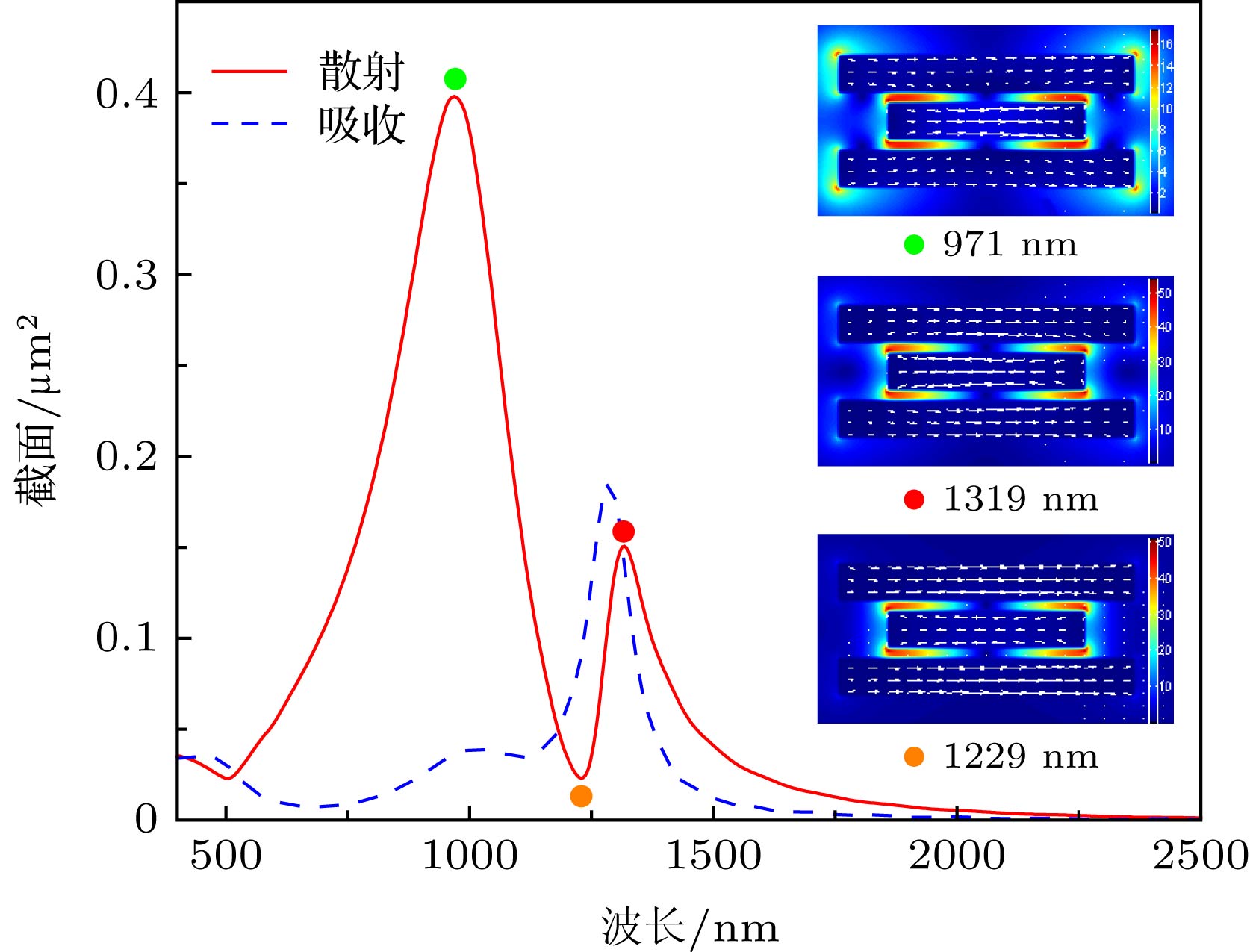
图 2 金纳米棒三聚体的散射谱和吸收谱, 插图为在两个散射共振峰位971, 1319和共振谷1229 nm处的纳米结构截面电场和电流密度矢量分布
Figure 2. Scattering and absorption spectra of a single gold nanorod trimer. Insets show the calculated electric field and current density vector distributions across the central cross section of the nanorod trimer at the indicated resonances.
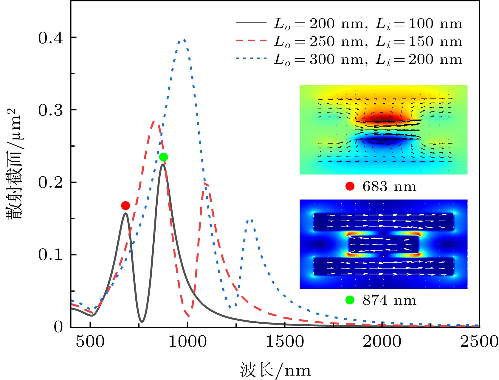
图 5 金纳米棒三聚体的散射谱随三棒尺寸变化的关系, 插图为在指定散射共振峰位处的纳米结构截面电磁场和电流密度矢量分布
Figure 5. Scattering spectra of the nanorod trimer versus the nanorod length with constant displacement ΔL = 100 nm. Insets show the calculated electric field, magnetic field in the z-direction and current density vector distributions at the indicated resonances.
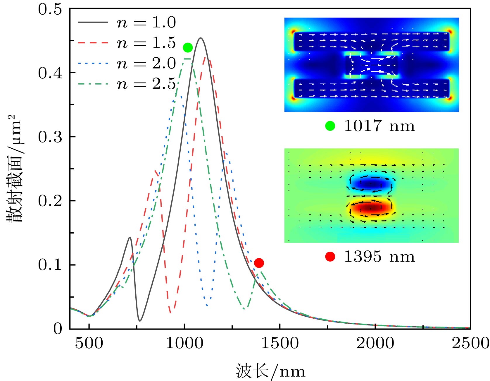
图 7 当短棒与边棒的间隙内介电环境变化时, 金纳米棒三聚体的散射谱随介质折射率变化的关系, 插图为在两个散射共振峰位处的纳米结构截面电磁场和电流密度矢量分布
Figure 7. Scattering spectra of the nanorod trimer with different media in the gaps between the center and side nanorods. Insets show the calculated electric field, magnetic field in the z-direction and current density vector distributions at the indicated resonances.
-
[1] Zhang S P, Xu H X 2016 Nanoscale 8 13722
 Google Scholar
[2] Biswas S, Duan J, Nepal D, Park K, Pachter R, Vaia R A 2013 Nano Lett. 13 6287
 Google Scholar
[3] Artar A, Yanik A A, Altug H 2011 Nano Lett. 11 3694
 Google Scholar
[4] Wu D, Liu C, Liu Y, Yu L, Yu Z, Chen L, Ma R, Ye H 2017 Opt. Lett. 42 450
 Google Scholar
[5] Zhang J, Chen S, Wang J,Mu K, Fan C, Liang E, Ding P 2018 Sci. Rep. 8 740
 Google Scholar
[6] Limonov M F, Rybin M V, Poddubny A N, Kivshar Y S 2017 Nat. Photon. 11 543
 Google Scholar
[7] Chen J, Gan F, Wang Y, Li G 2018 Adv. Opt. Mater. 6 1701152
 Google Scholar
[8] Huang C Y, Chang H C 2019 IEEE Photon. J. 11 4800208
 Google Scholar
[9] Li G Z, Hu H J, Wu L 2019 Phys. Chem. Chem. Phys. 21 7654
 Google Scholar
[10] Wu C, Khanikaev A B, Shvets G 2011 Phys. Rev. Lett. 106 107403
 Google Scholar
[11] Chang W S, Lassiter J B, Swanglap P, Sobhani H, Khatua S, Nordlander P, Halas N J, Link S 2012 Nano Lett. 12 4977
 Google Scholar
[12] Yu Y, Xue W, Semenova E, Yvind K, Mork J 2017 Nat. Photon. 11 81
 Google Scholar
[13] Hu H J, Zhang F W, Li G Z, Chen J Y, Li Q, Wu L J 2018 Photon. Res. 6 204
 Google Scholar
[14] Yang Z J, Hao Z H, Lin H Q, Wang Q Q 2014 Nanoscale 6 4985
 Google Scholar
[15] 黄运欢, 李璞 2015 物理学报 64 207301
 Google Scholar
Huang Y H, Li P 2015 Acta Phys. Sin. 64 207301
 Google Scholar
[16] Zhang Y, Jia T Q, Zhang H M, Xu Z Z 2012 Opt. Lett. 37 4919
 Google Scholar
[17] Fu Y H, Zhang J B, Yu Y F, Lukyanchuk B 2012 ACS Nano 6 5130
 Google Scholar
[18] Zhao W, Jiang Y 2015 Opt. Lett. 40 93
 Google Scholar
[19] Yang Z J, Wang Q Q, Lin H Q 2013 Appl. Phys. Lett. 103 111115
 Google Scholar
[20] Zhang S, Genov D A, Wang Y, Liu M, Zhang X 2008 Phys. Rev. Lett. 101 047401
 Google Scholar
[21] Wang J, Liu X, Li L, He J, Fan C, Tian Y, Ding P, Chen D, Xue Q, Liang E 2013 J. Opt. 15 105003
 Google Scholar
[22] Dong Z G, Liu H, Xu M X, Li Tao, Wang S M, Zhu S N, Zhang X 2010 Opt. Express 18 18229
 Google Scholar
[23] Jin X R, Park J, Zheng H, Lee S, Lee Y, Rhee J Y, Kim K W, Cheong H S, Jang W H 2011 Opt. Express 19 21652
 Google Scholar
[24] Bozhevolnyi S I, Evlyukhin A B, Pors A, Nielsen M G, Willatzen M, Albrektsen O 2011 New J. Phys. 13 023034
 Google Scholar
[25] Yang Z J, Zhang Z S, Zhang L H, Li Q Q, Hao Z H, Wang Q Q 2011 Opt. Lett. 36 1542
 Google Scholar
[26] Kai G, Zhang Y L, Qian C, Fung K H 2018 Opt. Express 26 11984
 Google Scholar
[27] Liu G D, Zhai X, Wang L L, Wang B X, Lin Q, Shang X J 2016 Plasmonics 11 381
 Google Scholar
[28] Liu S D, Leong E S P, Li G C, Hou Y, Deng J, Teng J H, Ong H C, Lei D Y 2016 ACS Nano 10 1442
 Google Scholar
[29] Wang J, Fan C, He J, Ding P, Liang E, Xue Q 2013 Opt. Express 21 2236
 Google Scholar
[30] Li G, Li Q, Xu L, Wu L 2015 Plasmonics 10 1401
 Google Scholar
[31] 丛超, 吴大建, 刘晓峻 2011 物理学报 60 046102
 Google Scholar
Cong C, Wu D J, Liu X J 2011 Acta Phys. Sin. 60 046102
 Google Scholar
[32] Taflove A, Hagness S 2000 Computational Electrodynamics: the Finite-Difference Time-Domain Method (Vol. 2) (Boston: Artech House) pp75−85
[33] Johnson P B, Christy R W 1972 Phys. Rev. B 6 4370
 Google Scholar
[34] Halas N J, Lal S, Chang W S, Nordlander P 2011 Chem. Rev. 111 3913
 Google Scholar
[35] Feng R, Qiu J, Liu L, Ding W, Chen L 2014 Opt. Express 22 A1713
 Google Scholar
[36] Hu X, Huang Y, Yuan S, Liu Y, Jiao Z, Wang Y, Huang Q, Yu J, Xia J 2015 Plasmonics 10 1817
 Google Scholar
Catalog
Metrics
- Abstract views: 12239
- PDF Downloads: 136
- Cited By: 0


 DownLoad:
