-
Optical pressure sensor plays a very important role in micro deformation detection, environmental monitoring, and medical fields. However, the quantitative relationship between the applied pressure and the optical response of the resonator before and after deformation is difficult to obtain. In this paper, a coupled resonator system based on metal-insulator-metal waveguide for optical pressure sensor is proposed. The mechanical properties of the system and the optical transmission properties before and after applied pressure are analyzed in detail by using the finite element method. Simulation results show that the maximum deformation of the resonator has a simple linear relationship with the applied pressure. We give a direct definition of the sensitivity of the optical pressure sensor. And based on the Fano resonance phenomenon caused by the coupling the slot cavity with the groove cavity, the optical pressure sensor with a sensitivity of 6.75 nm/MPa is achieved. In addition, we add stub resonator to obtain double Fano resonance phenomenon, and with the change of external pressure, the two Fano line types show different change laws. Specifically, a suitable pressure value can make a double Fano resonance become a single Fano resonance. The special features of our suggested structure are applicable to detecting optical property changes under different pressures, chemical high pressure experimental measurement and study of chemical reaction kinetics process.
-
Keywords:
- surface plasmon /
- metal-insulator-metal waveguide /
- optical pressure sensor /
- Fano resonance
[1] Wang J W, Sabcgez M M, Yin Y, Herzer R, Ma L B, Schmidt O G 2020 Adv. Materials Techno. 5 1901138
 Google Scholar
[2] Luan E, Shoman H, Ratner D M, Cheung K, Chrostowski L 2018 Sensors 18 3519
 Google Scholar
[3] Mejia J R, Oliveira O N 2018 Chem. Rev. 118 10617
 Google Scholar
[4] You B W, Lu J Y, Liu T A, Peng J L 2013 Opt. Express 21 21087
 Google Scholar
[5] Steglich P, Villringer C, Pulwer S 2017 IEEE Sensors J. 17 4781
 Google Scholar
[6] 肖功利, 张开富, 杨宏艳, 杨寓婷, 杨秀华, 窦婉滢, 曾丽珍 2020 光学学报 40 1206001
 Google Scholar
Xiao G L, Zhang K F, Yang H Y, Yang Y T, Yang X H, Dou W Y, Zeng L Z 2020 Acta Opt. Sin. 40 1206001
 Google Scholar
[7] Gandhi S, Awasthi S, Aly A 2021 RSC Adv. 11 26655
 Google Scholar
[8] Raschke G, Brogl S, Susha S, Rogach A, Klar T, Feldmann J, Fieres B, Petkov N, Bein T, Nichtl A, Kurzinger K 2004 Nano Lett. 4 1853
 Google Scholar
[9] Perfezou M, Turner A, Merkoci A 2012 Chem. Soc. Rev. 41 2606
 Google Scholar
[10] 旷依琴, 李刚, 闫竹青, 张彦军, 张志东, 郝现伟 2020 光学学报 40 1424001
 Google Scholar
Kuang Y Q, Li G, Yan Z Q, Zhang Y J, Zhang Z D, Hao X W 2020 Acta Opt. Sin. 40 1424001
 Google Scholar
[11] Nourinovin S, Nacarro M, Rahman M M 2022 IEEE Antenn. Propag. M. 64 60
 Google Scholar
[12] Bochenkov V E, Shabatina T I 2018 Biosensors 8 120
 Google Scholar
[13] Chen Z, Ma X X, Duan Y H, Li LH, Zhang S J, Wang Y L, Yu Y L, Hou Z L 2023 Opt. Express 31 35697
 Google Scholar
[14] 张燕君, 王护吉, 张龙图, 李广亮, 付兴虎 2022 光学学报 42 0524002
 Google Scholar
Zhang Y J, Wang H J, Zhang L T, Li G L, Fu X H 2022 Acta Opt. Sin. 42 0524002
 Google Scholar
[15] Chen J, Li Z, Zou Y 2013 Plasmonics 8 1627
 Google Scholar
[16] Wen K, Chen L, Zhou J 2018 Sensors 18 3181
 Google Scholar
[17] 韩帅涛, 陈颖, 许扬眉, 曹景刚, 高新贝, 谢进朝, 朱奇光 2019 光学学报 39 0212005
 Google Scholar
Han S T, Chen Y, Xu Y M, Cao J G, Gao X B, Xie J C, Zhu Q G 2019 Acta Optica Sinica 39 0212005
 Google Scholar
[18] Chau Y, Chao C, Huang H 2019 Nanomaterials 9 1433
 Google Scholar
[19] Tathfif I, Hassan M, Sharmeen K 2022 Opt. Commun. 519 128429
 Google Scholar
[20] Chen Z, Wang Y L, Hou Z L 2022 IEEE Sensors J. 22 14044
 Google Scholar
[21] Chaudhary V S, Kumar D, Mishra R 2020 Optik 210 164497
 Google Scholar
[22] Fu H, Tam H Y, Shao L Y 2008 Appl. Opt. 47 2835
 Google Scholar
[23] Chen F, Yang W X 2022 J. Opt. Soc. Am. B 39 1716
 Google Scholar
[24] Tathfif I, Yaseer A A, Rashid K S 2021 Opt. Express 29 32365
 Google Scholar
[25] Wu J, Lang P, Chen X 2016 J. Mod. Opt. 63 219
 Google Scholar
[26] Johnson P B, Christy R W 1972 Phys. Rev. B 6 4370
 Google Scholar
[27] Chen Z, Yu L, Wang L 2015 J. Light. Technolo. 33 3250
 Google Scholar
[28] Chen Z, Yu L, Wang L 2015 IEEE Photon. Techno. Lett. 27 1695
 Google Scholar
[29] Chen J J, Li Z, Li J, Gong Q H 2011 Opt. Express 19 9976
 Google Scholar
[30] Wu Y D 2014 J. Light. Techno. 32 4242
 Google Scholar
[31] Rohimah S, Tian H, Wang J 2022 Appl. Opt. 61 1275
 Google Scholar
[32] Chai Z, Hu X Y, Zhu Y, Sun S B, Yang H, Gong Q H 2014 Adv. Opt. Mater. 2 320
 Google Scholar
[33] Chai Z, Hu X Y, Yang H, Gong Q H 2016 Appl. Phys. Lett. 108 151104
 Google Scholar
-
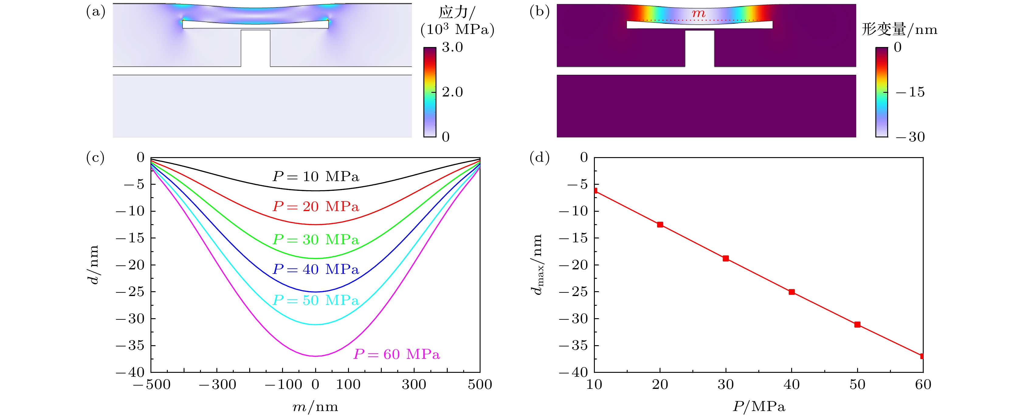
图 2 输入压力P = 50 MPa (a) 冯·米塞斯应力分布; (b) y-方向形变量分布示意图; (c) 不同输入压力P下形变量 d 沿图(b)中黑色虚线 m 的分布示意图; (d)最大形变量dmax与输入压力P的关系图
Figure 2. (a) Von Mises stress (a) and deformation displacement field y-component (b) distributions at P = 50 MPa; (c) distribution of deformation d along the black dashed line m in (b) at different input pressure P; (d) distribution of the maximum deformation dmax vs. input pressure P.
图 3 (a) 形变后的超细化三角形网格示意图; (b) 不同压力时, 系统的透射谱分布图; (c) P = 40 MPa时, 输入波长为λ = 1675 nm时的归一化|Hz|分布图(图(b)中粉色箭头所示位置)
Figure 3. (a) Extra-fine triangular meshing of the proposed structure model after deformation; (b) transmission spectra for different P; (c) normalized field distributions of |Hz| at λ = 1675 nm (showed by the pink arrow in Fig. (b)).
图 4 (a)插图中所示结构, 有无压力时的透射谱示意图, 黑色和红色曲线分别对应P = 0 MPa和P = 50 MPa时的情形; P = 50 MPa时, (b) λ = 1366 nm和(c) λ = 1790 nm, 两个Fano峰位置处的归一化|Hz|分布图, 图(a)中的插图为增加stub腔之后的结构示意图
Figure 4. (a) Transmission spectra of the inset structure with P = 0 MPa (black line) and P = 50 MPa (red line); normalized field distributions of |Hz| at (b) λ = 1366 nm and (c) λ = 1790 nm at P = 50 MPa. Inset shows the schematic diagram of the structure after adding a stub cavity.
-
[1] Wang J W, Sabcgez M M, Yin Y, Herzer R, Ma L B, Schmidt O G 2020 Adv. Materials Techno. 5 1901138
 Google Scholar
[2] Luan E, Shoman H, Ratner D M, Cheung K, Chrostowski L 2018 Sensors 18 3519
 Google Scholar
[3] Mejia J R, Oliveira O N 2018 Chem. Rev. 118 10617
 Google Scholar
[4] You B W, Lu J Y, Liu T A, Peng J L 2013 Opt. Express 21 21087
 Google Scholar
[5] Steglich P, Villringer C, Pulwer S 2017 IEEE Sensors J. 17 4781
 Google Scholar
[6] 肖功利, 张开富, 杨宏艳, 杨寓婷, 杨秀华, 窦婉滢, 曾丽珍 2020 光学学报 40 1206001
 Google Scholar
Xiao G L, Zhang K F, Yang H Y, Yang Y T, Yang X H, Dou W Y, Zeng L Z 2020 Acta Opt. Sin. 40 1206001
 Google Scholar
[7] Gandhi S, Awasthi S, Aly A 2021 RSC Adv. 11 26655
 Google Scholar
[8] Raschke G, Brogl S, Susha S, Rogach A, Klar T, Feldmann J, Fieres B, Petkov N, Bein T, Nichtl A, Kurzinger K 2004 Nano Lett. 4 1853
 Google Scholar
[9] Perfezou M, Turner A, Merkoci A 2012 Chem. Soc. Rev. 41 2606
 Google Scholar
[10] 旷依琴, 李刚, 闫竹青, 张彦军, 张志东, 郝现伟 2020 光学学报 40 1424001
 Google Scholar
Kuang Y Q, Li G, Yan Z Q, Zhang Y J, Zhang Z D, Hao X W 2020 Acta Opt. Sin. 40 1424001
 Google Scholar
[11] Nourinovin S, Nacarro M, Rahman M M 2022 IEEE Antenn. Propag. M. 64 60
 Google Scholar
[12] Bochenkov V E, Shabatina T I 2018 Biosensors 8 120
 Google Scholar
[13] Chen Z, Ma X X, Duan Y H, Li LH, Zhang S J, Wang Y L, Yu Y L, Hou Z L 2023 Opt. Express 31 35697
 Google Scholar
[14] 张燕君, 王护吉, 张龙图, 李广亮, 付兴虎 2022 光学学报 42 0524002
 Google Scholar
Zhang Y J, Wang H J, Zhang L T, Li G L, Fu X H 2022 Acta Opt. Sin. 42 0524002
 Google Scholar
[15] Chen J, Li Z, Zou Y 2013 Plasmonics 8 1627
 Google Scholar
[16] Wen K, Chen L, Zhou J 2018 Sensors 18 3181
 Google Scholar
[17] 韩帅涛, 陈颖, 许扬眉, 曹景刚, 高新贝, 谢进朝, 朱奇光 2019 光学学报 39 0212005
 Google Scholar
Han S T, Chen Y, Xu Y M, Cao J G, Gao X B, Xie J C, Zhu Q G 2019 Acta Optica Sinica 39 0212005
 Google Scholar
[18] Chau Y, Chao C, Huang H 2019 Nanomaterials 9 1433
 Google Scholar
[19] Tathfif I, Hassan M, Sharmeen K 2022 Opt. Commun. 519 128429
 Google Scholar
[20] Chen Z, Wang Y L, Hou Z L 2022 IEEE Sensors J. 22 14044
 Google Scholar
[21] Chaudhary V S, Kumar D, Mishra R 2020 Optik 210 164497
 Google Scholar
[22] Fu H, Tam H Y, Shao L Y 2008 Appl. Opt. 47 2835
 Google Scholar
[23] Chen F, Yang W X 2022 J. Opt. Soc. Am. B 39 1716
 Google Scholar
[24] Tathfif I, Yaseer A A, Rashid K S 2021 Opt. Express 29 32365
 Google Scholar
[25] Wu J, Lang P, Chen X 2016 J. Mod. Opt. 63 219
 Google Scholar
[26] Johnson P B, Christy R W 1972 Phys. Rev. B 6 4370
 Google Scholar
[27] Chen Z, Yu L, Wang L 2015 J. Light. Technolo. 33 3250
 Google Scholar
[28] Chen Z, Yu L, Wang L 2015 IEEE Photon. Techno. Lett. 27 1695
 Google Scholar
[29] Chen J J, Li Z, Li J, Gong Q H 2011 Opt. Express 19 9976
 Google Scholar
[30] Wu Y D 2014 J. Light. Techno. 32 4242
 Google Scholar
[31] Rohimah S, Tian H, Wang J 2022 Appl. Opt. 61 1275
 Google Scholar
[32] Chai Z, Hu X Y, Zhu Y, Sun S B, Yang H, Gong Q H 2014 Adv. Opt. Mater. 2 320
 Google Scholar
[33] Chai Z, Hu X Y, Yang H, Gong Q H 2016 Appl. Phys. Lett. 108 151104
 Google Scholar
Catalog
Metrics
- Abstract views: 4815
- PDF Downloads: 79
- Cited By: 0


 DownLoad:


