-
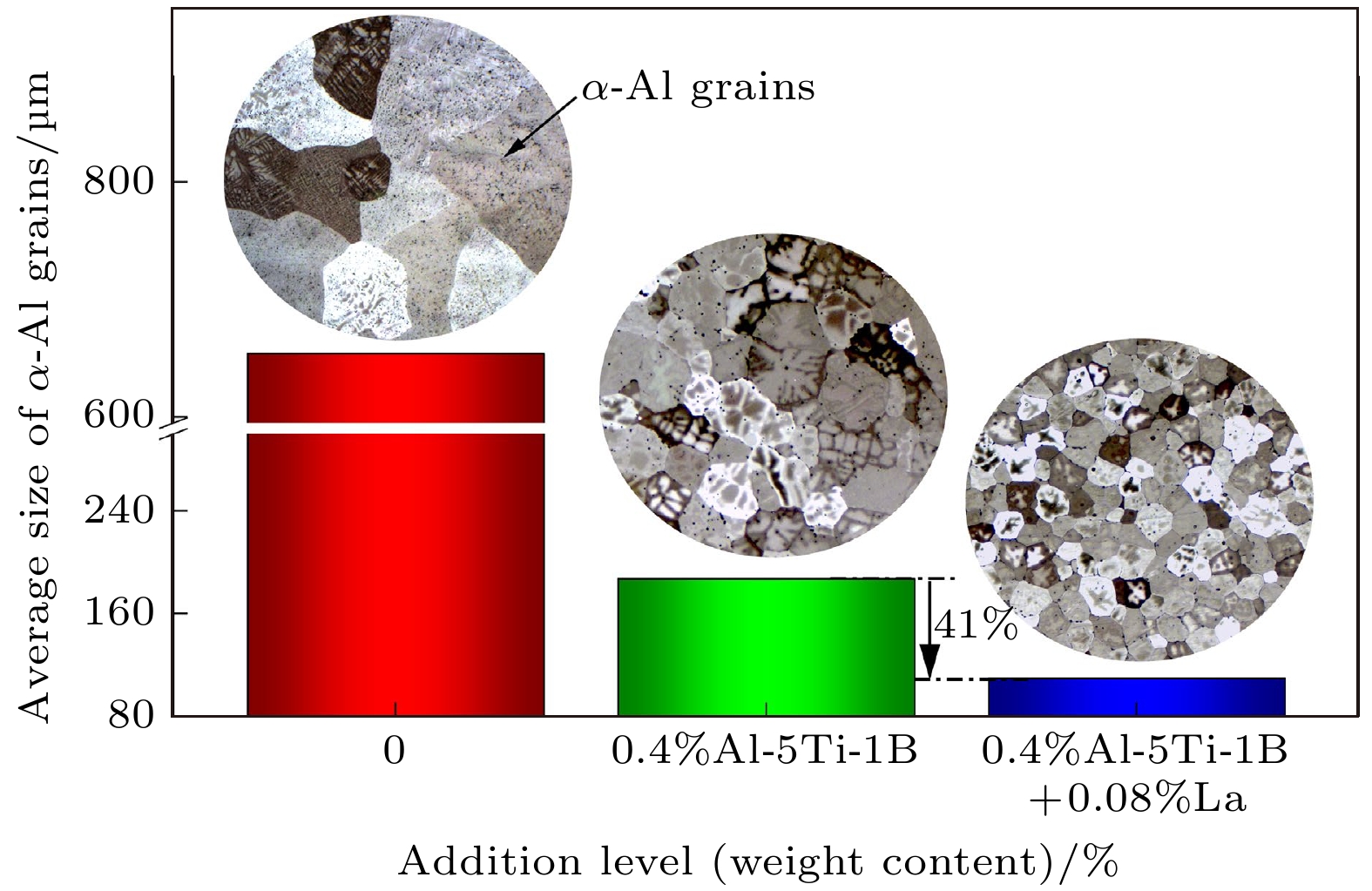
Grain refinement of aluminium alloys can not only reduce the defects (such as segregation and hot tearing) but also improve the mechanical properties. Adding Al-5Ti-1B master alloy to the melt has become a common method to refine the solidification microstructure of aluminium alloys. A lot of researches have been carried out to uncover the grain refining mechanisms as well as to show the microstructure formation under the effect of grain refiner. These researches demonstrated that the grain refining efficiency is closely related to the number density of TiB2 particles as well as the solute Ti concentration in the melt. However, there exist still problems to be resolved, such as the limited grain refinement potency of Al-5Ti-1B master alloy. Recently, the addition of trace La to the melt has attracted much attention to control the microstructure of aluminium alloys. The Al-Cu alloys are widely applied to the automobile and aerospace fields due to their high strength, good ductility and high temperature properties. It has been reported that Cu can segregate to Al/TiB2 interface in the Al-Cu melt inoculated with Al-5Ti-1B master alloy. But the effect of Cu segregation on the grain refinement result is not clear yet. Meanwhile, whether the grain refinement effect of Al-5Ti-1B master alloy on Al-Cu alloy can be improved by the addition of trace La has not been reported. Solidification experiments are carried out for Al-2Cu alloy with the addition of Al-5Ti-1B master alloy+ trace La. The synergistic effect of trace La and Al-5Ti-1B on the solidification microstructure of Al-2Cu alloy is investigated. It is found that trace La can effectively enhance the refinement result of Al-2Cu alloy and further diminish the nucleation undercooling. Experimental and calculated results demonstrate that solute Cu segregates to the Al/TiB2 interface and thus increases the interatomic spacing mismatch between Ti (0001) plane of the TiB2 particles and the interfacial monolayer, while La segregation reduces the interatomic spacing mismatch. The trace La addition reduces the interfacial energy between α-Al and TiB2 particles, improves the potency of TiB2 particles to nucleate α-Al, and thus enhances the grain refinement result of Al-5Ti-1B master alloy. -
Keywords:
- grain refinement /
- trace element /
- segregation /
- aluminium alloys
[1] 张丽丽 2017 博士学位论文 (沈阳: 中国科学院大学)
Zhang L L 2017 Ph. D. Dissertation (Shenyang: University of Chinese Academy of Sciences) (in Chinese)
[2] Greer A L, Bunn A M, Tronche A, Evans P V, Bristow D J 2000 Acta Mater. 48 2823
 Google Scholar
[3] Quested T E, Greer A L 2004 Acta Mater. 52 3859
 Google Scholar
[4] Quested T E, Greer A L 2005 Acta Mater. 53 4643
 Google Scholar
[5] Easton M A, StJohn D H 2001 Acta Mater. 49 1867
 Google Scholar
[6] Easton M A, StJohn D H 2005 Metall. Mater. Trans. A 36 1911
 Google Scholar
[7] Easton M A, StJohn D H 2008 Mater. Sci. Eng. A 486 8
 Google Scholar
[8] Fan Z, Wang Y, Zhang Y, Qin T, Zhou X R, Thompson G E, Pennycook T, Hashimoto T 2015 Acta Mater. 84 292
 Google Scholar
[9] Cibula A 1951 J. Inst. Met. 80 1
[10] Crossley F A, Mondolfo L F 1951 JOM. 3 1143
 Google Scholar
[11] Jones G P, Jones H 1987 Solidification Processing (Sheffield: University of Sheffield) p496
[12] Mohanty P S, Gruzleski J E 1995 Acta Metall. Mater. 43 2001
 Google Scholar
[13] Fan Z Y 2013 Metall. Mater. Trans. A 44 1409
 Google Scholar
[14] Maxwell I, Hellawell A 1975 Acta Metall. 23 229
 Google Scholar
[15] Zhang L L, Zheng Q J, Jiang H X, Zhao J Z 2019 Scr. Mater. 160 25
 Google Scholar
[16] Li J H, Hage F S, Ramasse Q M, Schumacher P 2021 Acta Mater. 206 116652
 Google Scholar
[17] 吴俊子, 贾锦玉, 姜佳鑫 2018 稀土信息 2 30
Wu J Z, Jia J Y, Jiang J X 2018 Rare Earth Inform. 2 30
[18] Han Y F 2007 Ph. D. Dissertation (Shanghai: Shanghai Jiao Tong University) (in Chinese)
[19] Zhang Z, Bian X, Wang Y, Liu, X 2003 Mater. Sci. Eng. A 352 8
 Google Scholar
[20] 李克, 饶磊, 闫洪, 王俊, 孙宝德 2006 铸造 9 894
Li K, Rao L, Yan H, Wang J, Sun B D 2006 Foundry 9 894
[21] 董天顺, 崔春翔, 刘双进, 刘福才 2008 稀有金属材料与工程 1 29
Dong T S, Cui C X, Liu S J, Liu F C 2008 Rare Metal Mater. Eng. 1 29
[22] Wang Z J, Si N C 2015 Rare Metal Mater. Eng. 44 2970
 Google Scholar
[23] Ma T F, Chen Z Y, Nie Z R, Huang H 2013 J. Rare Earths 31 622
 Google Scholar
[24] Wang K, Cui C X, Wang Q, Liu S, Gu C 2012 Mater. Lett. 85 153
 Google Scholar
[25] Wang K, Cui C X, Wang Q, Zhao L, Hu Y 2013 J. Rare Earths 31 313
 Google Scholar
[26] Zhang L L, Song Y, Yang L J, Zhao J Z, He J, Jiang H X 2022 Materials 15 600
 Google Scholar
[27] Zhang M X, Kelly P M, Easton M A, Taylor J A 2005 Acta Mater. 53 1427
 Google Scholar
[28] Wang Y, Fang C M, Zhou L, Hashimoto T, Fan Z 2018 Acta Mater. 164 428
 Google Scholar
[29] Iida T, Guthrie R I L 1993 The Physical Properties of Liquid Metals (Oxford: Clarendon Press) p71
[30] Fan T X, Yang G, Zhang D 2005 Metall. Mater. Trans. A 36 225
 Google Scholar
[31] Dinsdale A T 1991 Calphad. 15 317
 Google Scholar
[32] 李淑波, 杜文博, 王旭东, 刘轲, 王朝辉 2018 金属学报 54 911
 Google Scholar
Li S B, Du W B, Wang X D, Liu K, Wang C H 2018 Acta Metall. Sin. 54 911
 Google Scholar
[33] Zhang L L, Jiang H X, He J, Zhao J Z 2020 Scr. Mater. 179 99
 Google Scholar
[34] Okamoto H 2013 J. Phase Equilib. Diffus. 34 493
 Google Scholar
[35] Elliott R P, Shunk F A 1981 Bull. Alloy Phase Diagrams 2 219
 Google Scholar
-
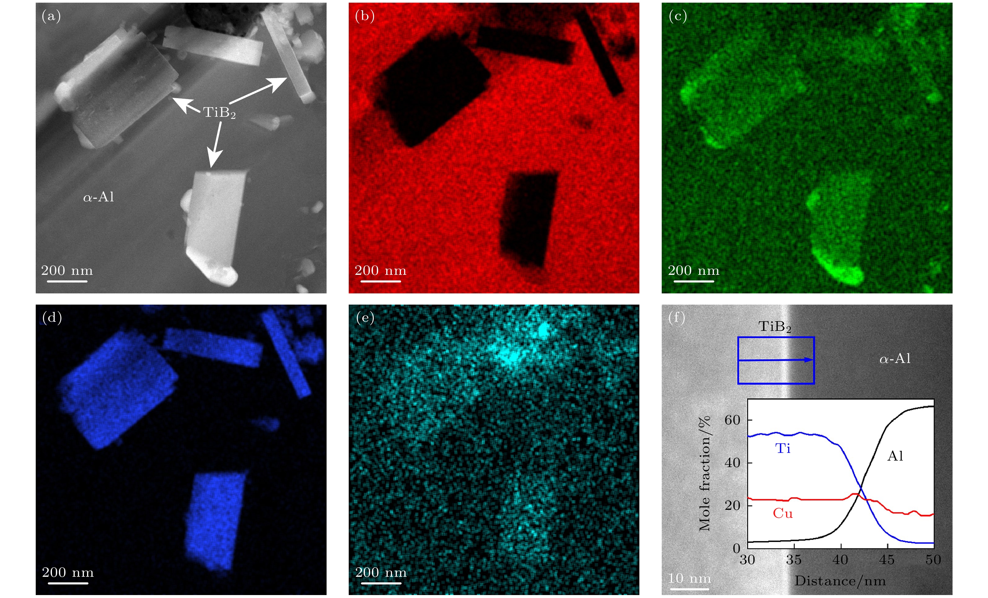
图 2 添加1% Al-5Ti-1B的Al-2Cu合金的TEM像及元素分布图 (a) 低倍TEM像; (b)—(e) 元素Al (b), Cu (c), Ti (d), B (e)分布图; (f) TiB2粒子的高倍TEM像, 其中插图为元素Al, Cu和Ti在蓝框内的平均电子能量损失谱线
Figure 2. TEM image and elemental maps in the Al-2Cu alloy inoculated by 1% Al-5Ti-1B: (a) TEM image at low magnification; (b)–(e) elemental maps of Al (b), Cu (c), Ti (d), B (e); (f) TEM image at high magnification of TiB2 particles, where inset shows the electron energy loss spectroscopy line profiles of elements Al, Cu and Ti averaged over the area indicated in Fig. (f) by blue box
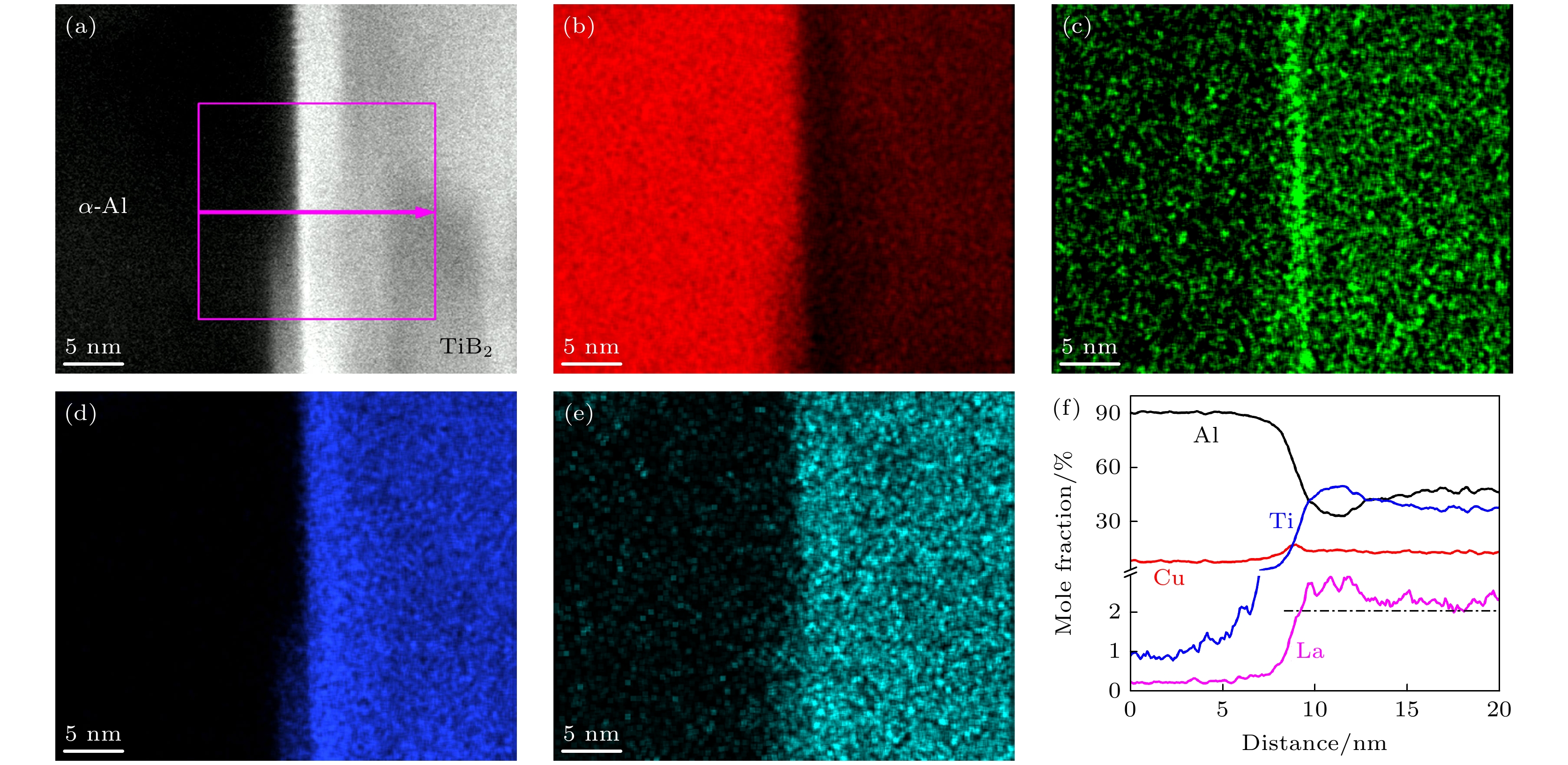
图 3 (a) 添加1% Al-5Ti-1B + 0.08% La的Al-2Cu合金的高倍TEM像; (b)—(e) 元素Al (b), Cu (c), Ti (d), La (e)的X射线能量散谱图; (f) Al, Cu, Ti和La元素的电子能量损失谱线
Figure 3. (a) TEM image at high magnification in Al-2Cu alloy inoculated by 1% Al-5Ti-1B + 0.08% La; (b)–(e) energy dispersive X-ray spectroscopy maps of Al (b), Cu (c), Ti (d), La (e); (f) electron energy loss spectroscopy line profiles of elements Al, Cu, Ti and La averaged over the area indicated in (a) by pink box of TiB2 particles.
图 4 添加1% Al-5Ti-1B + 0% La (a)和1% Al-5Ti-1B +0.08% La (b)的Al-2Cu合金HRTEM像; (c) TiB2粒子中Ti (0001)面与界面单原子层间界面示意图
Figure 4. HRTEM images showing the basal plane (0001) of TiB2 in Al-2Cu alloy inoculated with 1% Al-5Ti-1B + 0% La (a) and 1% Al-5Ti-1B +0.08%La (b), respectively; (c) schematic illustration of interface between the Ti (0001) plane of TiB2 surface and the monolayer
图 5 经0.4% Al-5Ti-1B细化处理的Al-2Cu合金的DTA升温(虚线)和冷却(实线)曲线, 其中Tm 和Tn分别为合金的熔点和开始形核温度, Tm = 926.2K; 插图为α-Al的形核过冷度ΔTHeter
Figure 5. DTA heating (dashed line) and cooling (solid line) curves for the Al-2Cu alloys with the addition of 0.4% Al-5Ti-1B master alloy. Tn and Tm = 926.2K are respectively the nucleation temperature of α-Al and the melting point temperature of Al. Inset shows the undercooling ΔTHeter.
-
[1] 张丽丽 2017 博士学位论文 (沈阳: 中国科学院大学)
Zhang L L 2017 Ph. D. Dissertation (Shenyang: University of Chinese Academy of Sciences) (in Chinese)
[2] Greer A L, Bunn A M, Tronche A, Evans P V, Bristow D J 2000 Acta Mater. 48 2823
 Google Scholar
[3] Quested T E, Greer A L 2004 Acta Mater. 52 3859
 Google Scholar
[4] Quested T E, Greer A L 2005 Acta Mater. 53 4643
 Google Scholar
[5] Easton M A, StJohn D H 2001 Acta Mater. 49 1867
 Google Scholar
[6] Easton M A, StJohn D H 2005 Metall. Mater. Trans. A 36 1911
 Google Scholar
[7] Easton M A, StJohn D H 2008 Mater. Sci. Eng. A 486 8
 Google Scholar
[8] Fan Z, Wang Y, Zhang Y, Qin T, Zhou X R, Thompson G E, Pennycook T, Hashimoto T 2015 Acta Mater. 84 292
 Google Scholar
[9] Cibula A 1951 J. Inst. Met. 80 1
[10] Crossley F A, Mondolfo L F 1951 JOM. 3 1143
 Google Scholar
[11] Jones G P, Jones H 1987 Solidification Processing (Sheffield: University of Sheffield) p496
[12] Mohanty P S, Gruzleski J E 1995 Acta Metall. Mater. 43 2001
 Google Scholar
[13] Fan Z Y 2013 Metall. Mater. Trans. A 44 1409
 Google Scholar
[14] Maxwell I, Hellawell A 1975 Acta Metall. 23 229
 Google Scholar
[15] Zhang L L, Zheng Q J, Jiang H X, Zhao J Z 2019 Scr. Mater. 160 25
 Google Scholar
[16] Li J H, Hage F S, Ramasse Q M, Schumacher P 2021 Acta Mater. 206 116652
 Google Scholar
[17] 吴俊子, 贾锦玉, 姜佳鑫 2018 稀土信息 2 30
Wu J Z, Jia J Y, Jiang J X 2018 Rare Earth Inform. 2 30
[18] Han Y F 2007 Ph. D. Dissertation (Shanghai: Shanghai Jiao Tong University) (in Chinese)
[19] Zhang Z, Bian X, Wang Y, Liu, X 2003 Mater. Sci. Eng. A 352 8
 Google Scholar
[20] 李克, 饶磊, 闫洪, 王俊, 孙宝德 2006 铸造 9 894
Li K, Rao L, Yan H, Wang J, Sun B D 2006 Foundry 9 894
[21] 董天顺, 崔春翔, 刘双进, 刘福才 2008 稀有金属材料与工程 1 29
Dong T S, Cui C X, Liu S J, Liu F C 2008 Rare Metal Mater. Eng. 1 29
[22] Wang Z J, Si N C 2015 Rare Metal Mater. Eng. 44 2970
 Google Scholar
[23] Ma T F, Chen Z Y, Nie Z R, Huang H 2013 J. Rare Earths 31 622
 Google Scholar
[24] Wang K, Cui C X, Wang Q, Liu S, Gu C 2012 Mater. Lett. 85 153
 Google Scholar
[25] Wang K, Cui C X, Wang Q, Zhao L, Hu Y 2013 J. Rare Earths 31 313
 Google Scholar
[26] Zhang L L, Song Y, Yang L J, Zhao J Z, He J, Jiang H X 2022 Materials 15 600
 Google Scholar
[27] Zhang M X, Kelly P M, Easton M A, Taylor J A 2005 Acta Mater. 53 1427
 Google Scholar
[28] Wang Y, Fang C M, Zhou L, Hashimoto T, Fan Z 2018 Acta Mater. 164 428
 Google Scholar
[29] Iida T, Guthrie R I L 1993 The Physical Properties of Liquid Metals (Oxford: Clarendon Press) p71
[30] Fan T X, Yang G, Zhang D 2005 Metall. Mater. Trans. A 36 225
 Google Scholar
[31] Dinsdale A T 1991 Calphad. 15 317
 Google Scholar
[32] 李淑波, 杜文博, 王旭东, 刘轲, 王朝辉 2018 金属学报 54 911
 Google Scholar
Li S B, Du W B, Wang X D, Liu K, Wang C H 2018 Acta Metall. Sin. 54 911
 Google Scholar
[33] Zhang L L, Jiang H X, He J, Zhao J Z 2020 Scr. Mater. 179 99
 Google Scholar
[34] Okamoto H 2013 J. Phase Equilib. Diffus. 34 493
 Google Scholar
[35] Elliott R P, Shunk F A 1981 Bull. Alloy Phase Diagrams 2 219
 Google Scholar
Catalog
Metrics
- Abstract views: 6258
- PDF Downloads: 88
- Cited By: 0


 DownLoad:


