-
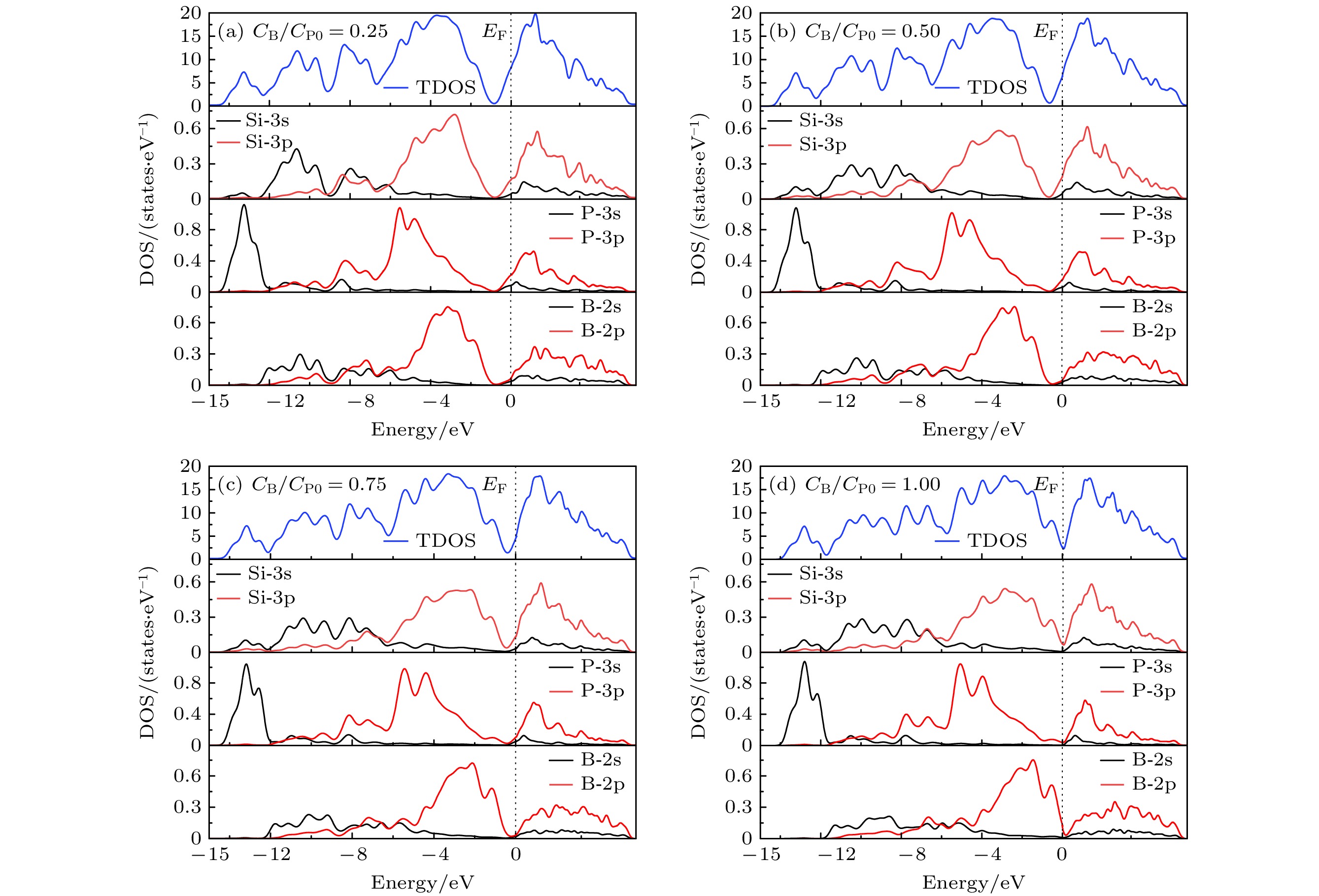
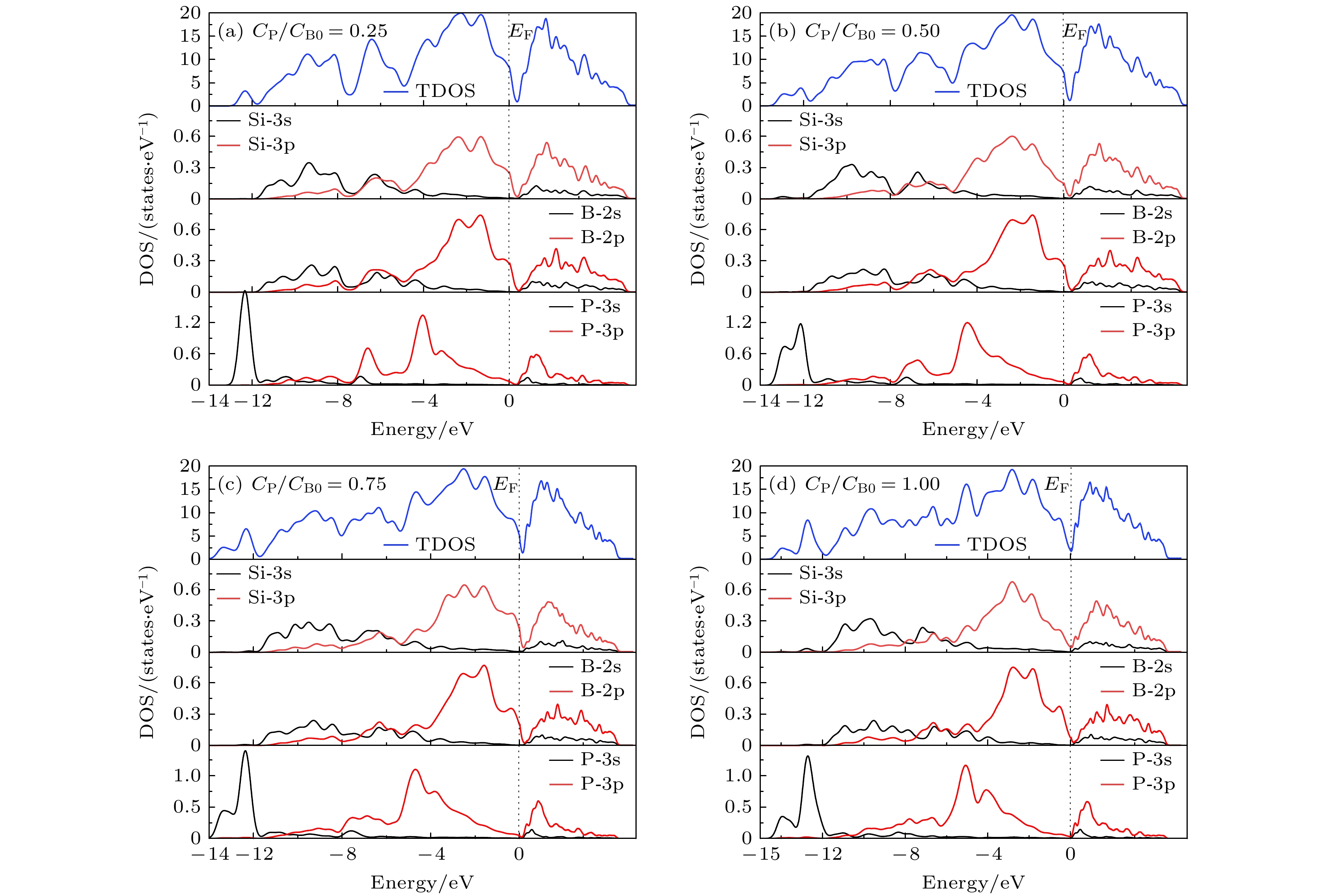
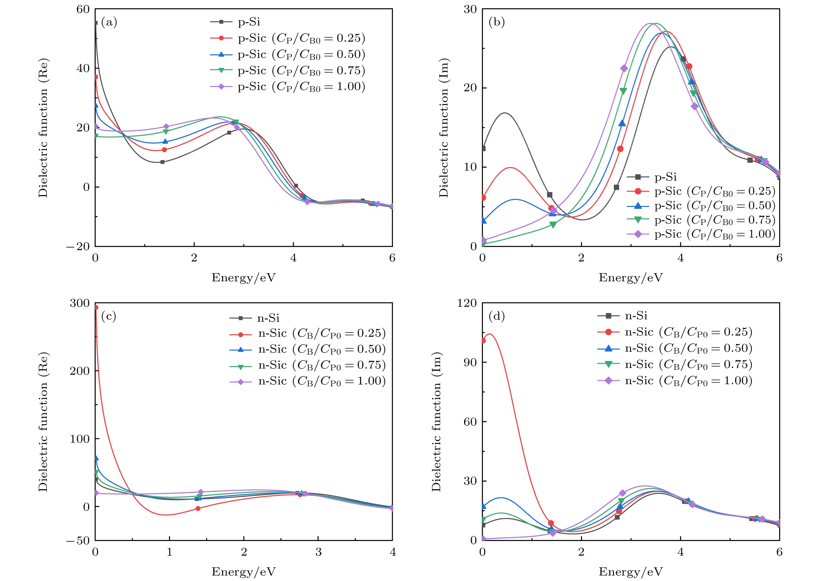
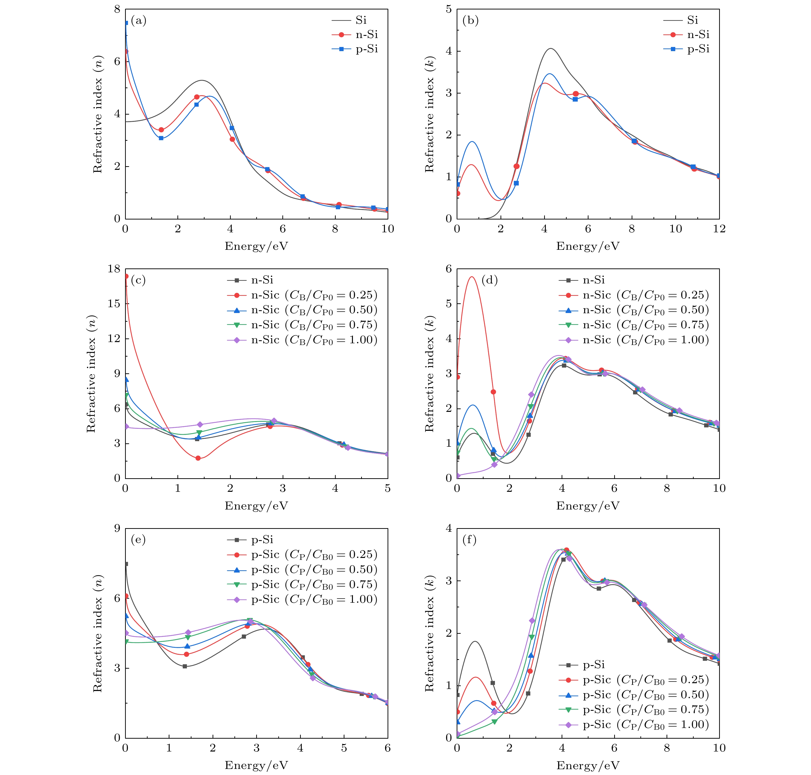
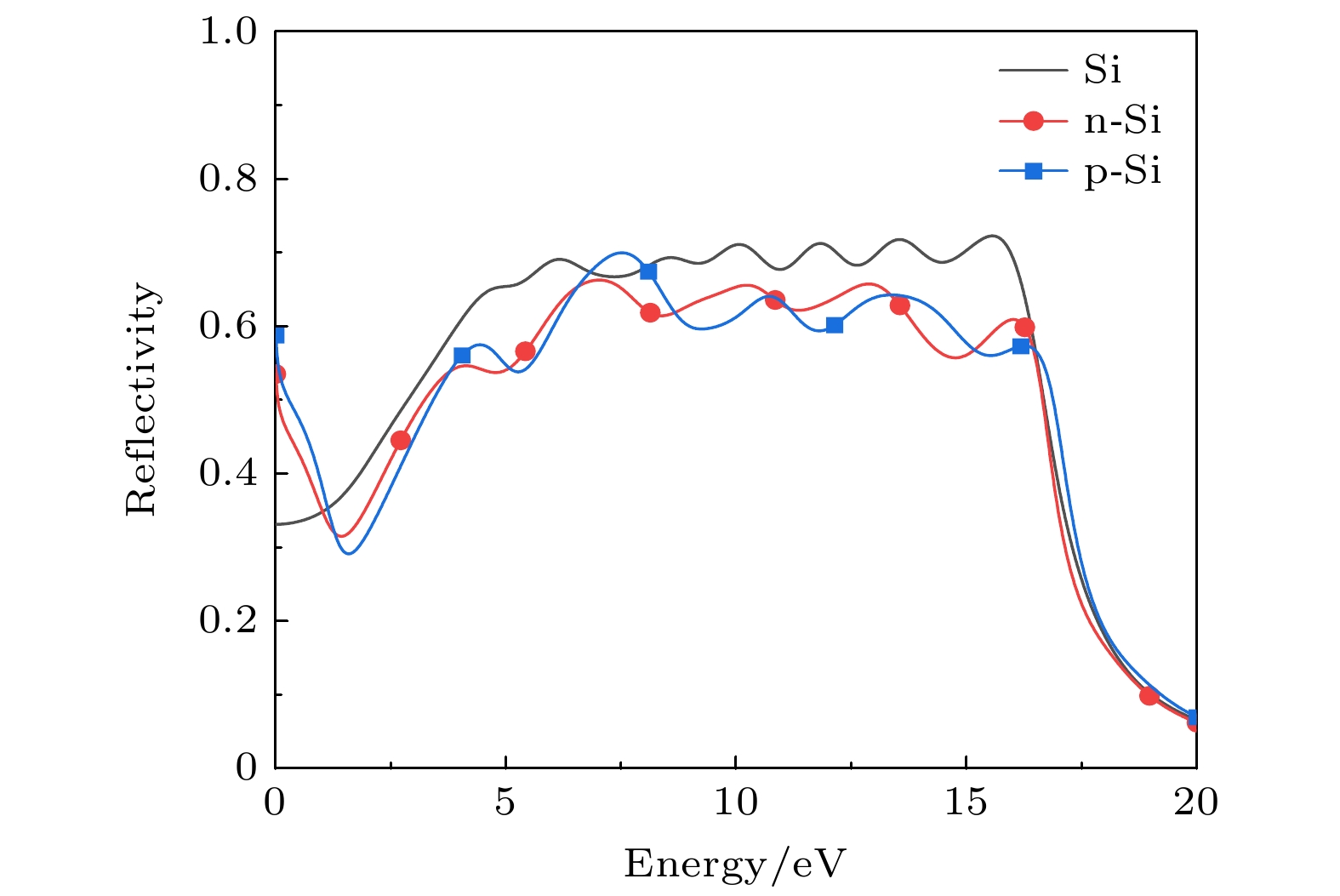
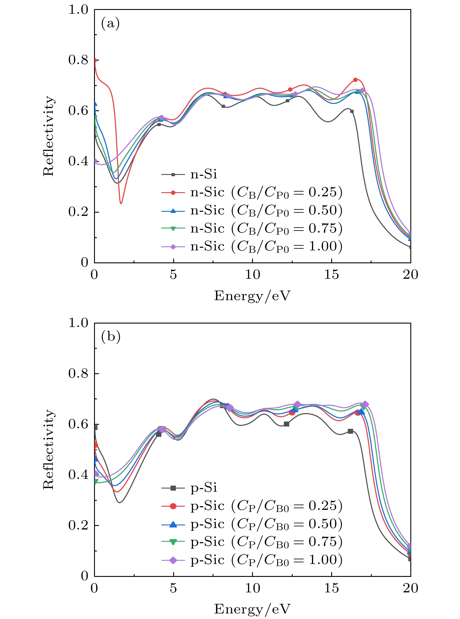
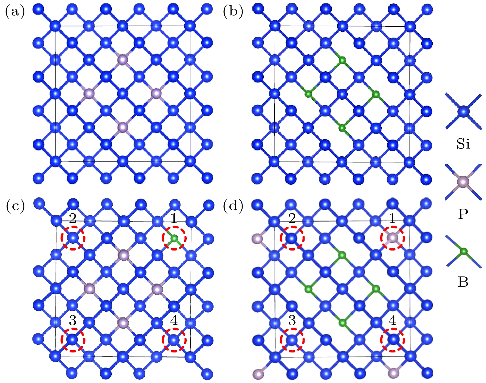
Presently, impurity-compensated silicon (Si) has no clear potential applications due to high resistance and few carriers. Thus, it has received little attention from researchers. In this study, we find that impurity compensation can make localized state energy levels form in Si bandgap, which can improve the light absorption of Si in the near infrared region. In this work, in order to comprehensively and deeply understand the photoelectric properties of impurity-compensated Si, the localized state energy levels composed of P+/B– ions are constructed in Si bandgap through the co-doping of phosphorus (P) and boron (B), thereby forming impurity-compensated Si. The first-principles based on a density functional theory framework is used to study the photoelectric properties of the impurity-compensated Si (n/p-Sic) such as the density of states (DOS), dielectric function and refractive index. The DOS study reveals the following results: after the n- and p-Si with the same concentration of P and B (12.5%) are fully compensated for by impurities, the Fermi energy levels of their compensated counterparts are at the valley bottom formed by the two adjacent DOS peaks, and the DOS is not zero at the valley bottom. In the study of dielectric function and refractive index, it is found that when the doping ratio is CB/CP0 = 0.25, n-Sic has the largest dielectric function and refractive index in the low energy region. In addition, comparing intrinsic Si with its doped counterparts in the real part (Re) of their dielectric constant, the following regularity is found: in the high energy region of E > 4 eV, the Re values of the intrinsic Si, n/p-Si and p-Sic are negative. In the low energy region of 0.64 eV< E < 1.50 eV, the Re value of n-Sic is negative for the doping ratio of CB/CP0 = 0.25. The above comparison indicates that the n-Sic with CB/CP0 = 0.25 can achieve good metallicity in the low energy region, indicating that the electrons in valence band are easily excited by low-energy long-wavelength light. Theoretical studies show that the good photoelectric properties of n-Sic with CB/CP0 = 0.25 may be related to Si dangling bonds and localized state energy levels in Si bandgap. The Si dangling bonds are caused by the impurity compensation of B dopant for n-Si, leading part of Si-Si bonds to change into Si-B bonds. This study provides theoretical guidance for the application of impurity-compensated Si in the field of photodetectors such as CMOS image sensors and infrared photodetectors.
-
Keywords:
- first-principles /
- density of states /
- impurity compensation /
- optical properties
[1] 萧宏著 (杨银堂, 段宝兴译) 2013 半导体制造技术导论 (北京: 电子工业出版社) 第428页
Xiao H (translated by Yang Y T, Duan B X) 2013 Introduction to Semiconductor Manufacturing Technology (Beijing: Publishing House of Electronic Industry) p428
[2] Soref R 2006 IEEE J. Sel. Top. Quantum Electron. 12 1678
 Google Scholar
[3] Li C, Zhao J H, Liu X H, Ren Z Y, Yang Y, Chen Z G, Chen Q D, Sun H B 2023 IEEE Trans. Electron Devices. 70 2364
 Google Scholar
[4] Ge X, Chen D, Cui X Y, Ma H B, Li Y, Chen Y L 2022 Proceedings of the 7th International Conference on Integrated Circuits and Microsystems, Xi'an, China October 28–31, 2022 p24
[5] 霍奇斯, 杰克逊, 萨利赫 著 (蒋安平, 王新安, 陈自力 译) 2005 数字集成电路分析与设计: 深亚微米工艺 (北京: 电子工业出版社) 第1页
Hodges D A, Jackson H G, Saleh R A (translated by Jiang A P, Wang X A, Chen Z L) 2005 Analysis and Design of Digital Integrated Circuits: In Deep Submicron Technology (Beijing: Publishing House of Electronic Industry) p1
[6] 刘恩科, 朱秉升, 罗晋生 2008 半导体物理学 (第七版) (北京: 电子工业出版社) 第41页
Liu E K, Zhu B S, Luo J S 2008 The Physics of Semiconductors (7th Ed.) (Beijing: Publishing House of Electronic Industry) p41
[7] Wang X Y, Wang T, Ren Q, Xu J T, Cui Y A 2023 Micro Nanostructures 184 207695
 Google Scholar
[8] Green M A 2008 Sol. Energy Mater. Sol. Cells 92 1305
 Google Scholar
[9] Pina J M, Vafaie M, Parmar D H, Atan O, Xia P, Zhang Y N, Najarian A M, Arquer F P G D, Hoogland S, Sargent E H 2022 Nano Lett. 22 6802
 Google Scholar
[10] Mailoa J P, Akey A J, Simmons C B, Hutchinson D, Mathews J, Sullivan J T, Recht D, Winkler M T, Williams J S, Warrender J M, Persans P D, Aziz M J, Buonassisi T 2014 Nat. Commun. 5 301
 Google Scholar
[11] Zhao J H, Li X B, Chen Q D, Chen Z G, Sun H B 2020 Mater. Today Nano 11 100078
 Google Scholar
[12] 韩冬, 孙飞阳, 鲁继远, 宋福明, 徐跃 2020 物理学报 69 148501
 Google Scholar
Han D, Sun F Y, Lu J Y, Song F M, Xu Y 2020 Acta Phys. Sin. 69 148501
 Google Scholar
[13] Ma J J, Fossum E R 2015 IEEE J. Electron Devices Soc. 3 73
 Google Scholar
[14] Larson L A, Williams J M, Current M I 2011 Rev. Accel. Sci. Technol. 04 11
 Google Scholar
[15] Yokogawa S, Oshiyama I, Ikeda H, Ebiko Y, Hirano T, Saito S, Oinoue T, Hagimoto Y, Iwamoto H 2017 Sci. Rep. 7 3832
 Google Scholar
[16] Khabir M, Alaibakhsh H, Karami M A 2021 Appl. Opt. 60 9640
 Google Scholar
[17] Li F, Wang R S, Han L Q, Xu J T 2020 J. Semicond. 41 102301
 Google Scholar
[18] Yang Y Y, Gong P, Ma W D, Hao R, Fang X Y 2021 Chin. Phys. B 30 067803
 Google Scholar
[19] Yang L Z, Liu W K, Yan H, Yu X X, Gong P, Li Y L, Fang X Y 2024 Eur. Phys. J. Plus 139 66
 Google Scholar
[20] Wang X Y, Liu Y P, Ding B N, Li M X, Chen T N, Zhu X T 2017 Superlattices Microstruct. 109 217
 Google Scholar
[21] Jia Y H, Gong P, Li S L, Ma W D, Fang X Y, Yang Y Y, Cao M S 2020 Phys. Lett. A 384 126106
 Google Scholar
[22] Ma Y, Yan H, Yu X X, Gong P, Li Y L, Ma W D, Fang X Y 2024 J. Appl. Phys. 135 054101
 Google Scholar
[23] 张晏蜜, 曹妍, 杨胭脂, 李佳龙, 廖杨芳 2021 低温物理学报 43 0135
 Google Scholar
Zhang Y M, Cao Y, Yang Y Z, Li J L, Liao Y F 2021 Low Temp. Phys. Lett. 43 0135
 Google Scholar
[24] Moore C, Adhikari C M, Das T, Resch L, Ullrich C A, Jentschura U D 2022 Phys. Rev. B 106 045202
 Google Scholar
[25] Kong S S, Liu W K, Yu X X, Li Y L, Yang L Z, Ma Y, Fang X Y 2023 Front. Phys. 18 43302
 Google Scholar
[26] Green M A, Keevers M J 1995 Prog. Photovoltaics Res. Appl. 3 189
 Google Scholar
[27] Yamaguchi T 1975 Appl. Opt. 14 1111
 Google Scholar
[28] 余志强 2012 物理学报 61 217102
 Google Scholar
Yu Z Q 2012 Acta Phys. Sin. 61 217102
 Google Scholar
[29] Diez M, Ametowobla M, Graf T 2017 J. Laser Micro/ Nanoeng. 12 230
 Google Scholar
-
-
[1] 萧宏著 (杨银堂, 段宝兴译) 2013 半导体制造技术导论 (北京: 电子工业出版社) 第428页
Xiao H (translated by Yang Y T, Duan B X) 2013 Introduction to Semiconductor Manufacturing Technology (Beijing: Publishing House of Electronic Industry) p428
[2] Soref R 2006 IEEE J. Sel. Top. Quantum Electron. 12 1678
 Google Scholar
[3] Li C, Zhao J H, Liu X H, Ren Z Y, Yang Y, Chen Z G, Chen Q D, Sun H B 2023 IEEE Trans. Electron Devices. 70 2364
 Google Scholar
[4] Ge X, Chen D, Cui X Y, Ma H B, Li Y, Chen Y L 2022 Proceedings of the 7th International Conference on Integrated Circuits and Microsystems, Xi'an, China October 28–31, 2022 p24
[5] 霍奇斯, 杰克逊, 萨利赫 著 (蒋安平, 王新安, 陈自力 译) 2005 数字集成电路分析与设计: 深亚微米工艺 (北京: 电子工业出版社) 第1页
Hodges D A, Jackson H G, Saleh R A (translated by Jiang A P, Wang X A, Chen Z L) 2005 Analysis and Design of Digital Integrated Circuits: In Deep Submicron Technology (Beijing: Publishing House of Electronic Industry) p1
[6] 刘恩科, 朱秉升, 罗晋生 2008 半导体物理学 (第七版) (北京: 电子工业出版社) 第41页
Liu E K, Zhu B S, Luo J S 2008 The Physics of Semiconductors (7th Ed.) (Beijing: Publishing House of Electronic Industry) p41
[7] Wang X Y, Wang T, Ren Q, Xu J T, Cui Y A 2023 Micro Nanostructures 184 207695
 Google Scholar
[8] Green M A 2008 Sol. Energy Mater. Sol. Cells 92 1305
 Google Scholar
[9] Pina J M, Vafaie M, Parmar D H, Atan O, Xia P, Zhang Y N, Najarian A M, Arquer F P G D, Hoogland S, Sargent E H 2022 Nano Lett. 22 6802
 Google Scholar
[10] Mailoa J P, Akey A J, Simmons C B, Hutchinson D, Mathews J, Sullivan J T, Recht D, Winkler M T, Williams J S, Warrender J M, Persans P D, Aziz M J, Buonassisi T 2014 Nat. Commun. 5 301
 Google Scholar
[11] Zhao J H, Li X B, Chen Q D, Chen Z G, Sun H B 2020 Mater. Today Nano 11 100078
 Google Scholar
[12] 韩冬, 孙飞阳, 鲁继远, 宋福明, 徐跃 2020 物理学报 69 148501
 Google Scholar
Han D, Sun F Y, Lu J Y, Song F M, Xu Y 2020 Acta Phys. Sin. 69 148501
 Google Scholar
[13] Ma J J, Fossum E R 2015 IEEE J. Electron Devices Soc. 3 73
 Google Scholar
[14] Larson L A, Williams J M, Current M I 2011 Rev. Accel. Sci. Technol. 04 11
 Google Scholar
[15] Yokogawa S, Oshiyama I, Ikeda H, Ebiko Y, Hirano T, Saito S, Oinoue T, Hagimoto Y, Iwamoto H 2017 Sci. Rep. 7 3832
 Google Scholar
[16] Khabir M, Alaibakhsh H, Karami M A 2021 Appl. Opt. 60 9640
 Google Scholar
[17] Li F, Wang R S, Han L Q, Xu J T 2020 J. Semicond. 41 102301
 Google Scholar
[18] Yang Y Y, Gong P, Ma W D, Hao R, Fang X Y 2021 Chin. Phys. B 30 067803
 Google Scholar
[19] Yang L Z, Liu W K, Yan H, Yu X X, Gong P, Li Y L, Fang X Y 2024 Eur. Phys. J. Plus 139 66
 Google Scholar
[20] Wang X Y, Liu Y P, Ding B N, Li M X, Chen T N, Zhu X T 2017 Superlattices Microstruct. 109 217
 Google Scholar
[21] Jia Y H, Gong P, Li S L, Ma W D, Fang X Y, Yang Y Y, Cao M S 2020 Phys. Lett. A 384 126106
 Google Scholar
[22] Ma Y, Yan H, Yu X X, Gong P, Li Y L, Ma W D, Fang X Y 2024 J. Appl. Phys. 135 054101
 Google Scholar
[23] 张晏蜜, 曹妍, 杨胭脂, 李佳龙, 廖杨芳 2021 低温物理学报 43 0135
 Google Scholar
Zhang Y M, Cao Y, Yang Y Z, Li J L, Liao Y F 2021 Low Temp. Phys. Lett. 43 0135
 Google Scholar
[24] Moore C, Adhikari C M, Das T, Resch L, Ullrich C A, Jentschura U D 2022 Phys. Rev. B 106 045202
 Google Scholar
[25] Kong S S, Liu W K, Yu X X, Li Y L, Yang L Z, Ma Y, Fang X Y 2023 Front. Phys. 18 43302
 Google Scholar
[26] Green M A, Keevers M J 1995 Prog. Photovoltaics Res. Appl. 3 189
 Google Scholar
[27] Yamaguchi T 1975 Appl. Opt. 14 1111
 Google Scholar
[28] 余志强 2012 物理学报 61 217102
 Google Scholar
Yu Z Q 2012 Acta Phys. Sin. 61 217102
 Google Scholar
[29] Diez M, Ametowobla M, Graf T 2017 J. Laser Micro/ Nanoeng. 12 230
 Google Scholar
Catalog
Metrics
- Abstract views: 5913
- PDF Downloads: 175
- Cited By: 0


 DownLoad:
