


-
目前Si基半导体由于其自身材料特性的限制, 已经越来越难以满足高速发展的现代电力电子技术对半导体器件的性能要求. SiC作为新一代半导体材料具有显著的性能优势, 但由于其属于典型的难加工材料, 实现SiC晶圆的高质量与高效率加工成为了推动其产业化应用进程的关键. 本综述在回顾近年来SiC超精密加工技术研究进展的基础上, 重点介绍了一种基于等离子体氧化改性的SiC高效超精密抛光技术, 分析了该技术的材料去除机理、典型装置、改性过程及抛光效果. 分析结果表明, 该技术具有较高的去除效率, 能够获得原子级平坦表面, 并且不会产生亚表面损伤. 同时针对表面改性辅助抛光技术加工SiC表面过程中出现的台阶现象, 探讨了该台阶结构的产生机理及调控策略. 最后对等离子体辅助抛光技术的发展与挑战进行了展望.
-
关键词:
- 单晶SiC /
- 原子及近原子尺度制造 /
- 等离子体 /
- 表面改性
At present, owing to the inherent limitations of the material characteristics of Si based semiconductor materials, Si based semiconductors are facing more and more challenges in meeting the performance requirements of the rapidly developing modern power electronic technologies used in semiconductor devices. As a new generation of semiconductor material, SiC has significant performance advantages, but it is difficult to process the SiC wafers with high-quality and high-efficiency in their industrial application. Reviewing the research progress of ultra-precision machining technology of SiC in recent years, we introduce plasma oxidation modification based highly efficient polishing technology of SiC in this paper. The material removal mechanism, typical device, modification process, and polishing result of this technology are analyzed. The analysis shows that the plasma oxidation modification possesses high removal efficiency and atomically flat surfaces without surface or subsurface damages. Furthermore, aiming at step-terrace structures produced during SiC surface processing with different polishing technologies, the generation mechanism and control strategy of periodic atomic layer step-terrace structures are discussed. Finally, the development and challenge of plasma-assisted polishing technology are prospected.-
Keywords:
- single crystal SiC /
- atomic and close-to-atomic scale manufacturing /
- plasma /
- surface modification
[1] Bencherif H, Pezzimenti F, Dehimi L, Della C 2020 Appl. Phys. A 126 854
 Google Scholar
[2] Haddud A, Desouza A, Khare A, Lee H 2017 J. Manuf. Technol. Mana. 28 1055
Google Scholar
[3] He Y, Clark G, Schaibley J, He Y, Chen M, Wei Y, Ding X, Zhang Q, Yao W, Xu X, Lu C, Pan J 2015 Nat. Nanotechnol. 10 497
Google Scholar
[4] Mohammed M 2020 Plasmonics 15 1989
Google Scholar
[5] Kim S, Ahn H, Lim J, Lee K 2019 J. Korean Phys. Soc. 74 196
Google Scholar
[6] Kimura M, Koga Y, Nakanishi H, Matsuda T, Kameda T, Nakashima Y 2017 IEEE J. Electron Devi. 6 100
Google Scholar
[7] Zhang Q, Cheng L, Boutaba R 2010 J. Internet. Serv. Appl. 1 7
Google Scholar
[8] Umezawa H, Nagase M, Kato Y, Shikata S 2012 Diam. Relat. Mater. 24 201
Google Scholar
[9] Sharofidinov S, Kukushkin S, Redkov A, Grashchenko A, Osipov A 2019 Tech. Phys. Lett. 45 711
Google Scholar
[10] Domnich V, Aratyn Y, Kriven W, Gogotsi Y 2008 Rev. Adv. Mater. Sci. 17 33
[11] Qian J, Voronin G, Zerda T, He D, Zhao Y 2002 J. Mater. Res. 17 2153
Google Scholar
[12] Casady J, Johnson R 1996 Solid State Electron. 39 1409
Google Scholar
[13] Luo Q, Lu J, Xu X 2016 Wear 350/351 99
Google Scholar
[14] Li N, Ding J, Xuan Z, Huang J, Lin Z 2018 Strength Mater. 50 419
Google Scholar
[15] Dai S, Lei H, Fu J 2020 J. Electron. Mater. 49 1301
Google Scholar
[16] Heydemann V, Everson W, Gamble R, Snyder D, Skowronski M 2004 Mater. Sci. Forum 457/460 805
Google Scholar
[17] Zhou L, Audurier V, Pirouz P, Powell J 1997 J. Electrochem. Soc. 144 161
Google Scholar
[18] Pan G, Zhou Y, Luo G, Shi X, Zou C, Gong H 2013 J. Mater. Sci. Mater. Electron. 24 5040
Google Scholar
[19] Kato T, Wada K, Hozomi E, Taniguchi H, Miura T, Nishizawa S, Arai K 2007 Mater. Sci. Forum 556/557 753
Google Scholar
[20] Neslen C, Mitchel W, Hengehold R 2001 J. Electron. Mater. 30 1271
Google Scholar
[21] Lee H, Kim M, Jeong H 2015 Int. J. Precis. Eng. Manuf. 16 2611
Google Scholar
[22] Lee H, Kim D, An J, Lee H, Kim K, Jeong H 2010 CIRP Ann. Manuf. Techn. 59 333
[23] Kurokawa S, Doi T, Wang C, Sano Y, Aida H, Oyama K, Takahashi K 2014 ECS Trans. 60 641
Google Scholar
[24] Zhou Y, Pan G S, Shi X L, Gong H, Luo G H, Gu Z H 2014 Surf. Coat. Tech. 251 48
Google Scholar
[25] Shi X L, Pan G S, Zhou Y, Gu Z H, Gong H, Zou C L 2014 Appl. Surf. Sci. 307 414
Google Scholar
[26] Liang H, Yan Q, Lu J, Luo B, Xiao X 2019 Int. J. Adv. Manuf. Tech. 103 1337
Google Scholar
[27] Zhai W J, Gao B, Chang J, Wang H 2019 Nanomanuf. Metrol. 2 36
Google Scholar
[28] 路家斌, 熊强, 阎秋生, 王鑫, 廖博涛 2019 表面技术 48 148
Lu J B, Xiong Q, Yan Q S, Wang X, Liao B T 2019 Surf. Tech. 48 148
[29] Murata J, Yodogawa K, Ban K 2017 Int. J. Mach. Tool. Manu. 114 1
[30] Shen X, Tu Q, Deng H, Jiang G, He X, Liu B, Yamamura K 2016 Appl. Phys. A 122 354
Google Scholar
[31] Deng H, Hosoya K, Imanishi Y, Endo K, Yamamura K 2015 Electrochem. Commun. 52 5
Google Scholar
[32] Kubota A, Yoshimura M, Fukuyama S, Iwamoto C, Touge M 2012 Precis. Eng. 36 137
Google Scholar
[33] Kubota A, Yagi K, Murata J, Yasui H, Miyamoto S, Hara H, Sano Y, Yamauchi K 2009 J. Electron. Mater. 38 159
Google Scholar
[34] Zhang P, Feng X, Yang J 2014 J. Semicond. 35 166
[35] Nitta H, Isobe A, Hong P, Hirao T 2011 Jpn. J. Appl. Phys. 50 046501
Google Scholar
[36] Kubota A, Fukuyama S, Ichimori Y, Touge M 2012 Diam. Relat. Mater. 24 59
Google Scholar
[37] Ballarin N, Carraro C, Maboudian R, Magagnin L 2014 Electrochem. Commun. 40 17
Google Scholar
[38] Lin Y, Kao C 2005 Int. J. Adv. Manuf. Tech. 25 33
Google Scholar
[39] Yamamura K, Takiguchi T, Ueda M, Hattori A, Zettsu N 2010 Adv. Mat. Res. 126-128 423
Google Scholar
[40] Yamamura K, Takiguchi T, Ueda M, Deng H, Hattori A, Zettsu N 2011 CIRP Ann. Manuf. Techn. 60 571
Google Scholar
[41] Mori Y, Yamamura K, Sano Y 2004 Rev. Sci. Instrum. 75 942
Google Scholar
[42] Sano Y, Yamamura K, Mimura H, Yamauchi K, Mori Y 2007 Rev. Sci. Instrum. 78 086102
Google Scholar
[43] Yamamura K, Ueda K, Nagano M, Zettsu N, Maeo S, Shimada S, Utaka T, Taniguchi K 2010 Nucl. Instrum. Meth. A 616 281
Google Scholar
[44] Sun R, Yang X, Watanabe K, Miyazaki S, Fukano T, Kitada M, Arima K, Kawai K, Yamamura K 2019 Nanomanuf. Metrol. 2 168
Google Scholar
[45] Deng H 2016 Ph. D. Dissertation (Osaka: Osaka University)
[46] Harb T, Kedzierski W, McConkey J 2001 J. Chem. Phys. 115 5507
Google Scholar
[47] Krstulovic N, Labazan I, Milosevic S, Cvelbar U, Vesel A, Mozetic M 2006 J. Phys. D: Appl. Phys. 39 3799
Google Scholar
[48] Deng H, Yamamura K 2013 CIRP Ann. Manuf. Techn. 62 575
Google Scholar
[49] Deng H, Ueda M, Yamamura K 2014 Int. J. Adv. Manuf. Tech. 72 1
[50] 张海霞, 张泰华, 郇勇 2003 微纳电子技术 40 245
Google Scholar
Zhang H X, Zhang T H, Huan Y 2003 Micronanoelectron. Tech. 40 245
Google Scholar
[51] Ashida K, Dojima D, Kutsuma Y, Torimi S, Nogami S, Imai Y, Kimura S, Mizuki J, Ohtani N, Kaneko T 2016 MRS Advances 1 3697
Google Scholar
[52] Lakhdari F, Belkhir N, Bouzid D, Herold V 2019 Int. J. Adv. Manuf. Tech. 102 1421
Google Scholar
[53] Deng H, Takiguchi T, Ueda M, Hattori1 A, Zettsu N, Yamamura K 2011 Jpn. J. Appl. Phys. 50 08JG05
[54] Palmieri R, Radtke C, Boudinov H, Silva E 2009 Appl. Phys. Lett. 95 113504
Google Scholar
[55] Shi X, Pan G, Zhou Y, Zou C, Gong H 2013 Appl. Surf. Sci. 284 195
Google Scholar
[56] Shi X, Pan G, Zhou Y, Xu L, Zou C, Gong H 2015 Surf. Coat. Tech. 270 206
Google Scholar
[57] Okamoto T, Sano Y, Tachibana K, Arima K, Hattori A, Yagi K, Murata J, Sadakuni S, Yamauchiet K 2011 J. Nanosci. Nanotechno. 11 2928
Google Scholar
[58] Hara H, Sano Y, Mimura H, Arima K, Kubota A, Yagi K, Murata J, Yamauchi K 2006 J. Electron. Mater. 35 11
Google Scholar
[59] Kubota A, Mimura H, Inagaki K, Arima K, Mori Y, Yamauchi K 2005 J. Electron. Mater. 34 439
Google Scholar
[60] Okamoto T, Sano Y, Hara H, Mimura H, Arima K, Yagi K, Murata J, Yamauchi K 2009 Mater. Sci. Forum 600-603 835
[61] Okamoto T, Sano Y, Hara H, Hatayama T, Arima K, Yagi K, Murata J, Sadakuni S, Tachibana K, Shirasawa Y, Mimura H, Fuyuki T, Yamauchi K 2010 Mater. Sci. Forum 645-648 775
[62] Deng H, Endo K, Yamamura K 2013 Appl. Phys. Lett. 103 111603
Google Scholar
[63] Deng H, Endo K, Yamamura K 2014 Appl. Phys. Lett. 104 101608
Google Scholar
[64] Deng H, Monna K, Tabata T, Endo K, Yamamura K 2014 CIRP Ann. Manuf. Techn. 63 529
Google Scholar
[65] Deng H, Endo K, Yamamura K 2015 Sci. Rep. 5 8947
Google Scholar
[66] Rokicki R, Hryniewicz R 2012 T. I. Met. Finish. 90 188
Google Scholar
[67] Suratwala T, Steele W, Wong L, Feit M, Miller P, Spears R, Shen N, Desjardin R 2015 J. Am. Ceram. Soc. 98 2395
Google Scholar
[68] Shaw J, Heine V 1990 J. Phys. Condens. Mater. 2 4351
Google Scholar
[69] Chien F, Nutt S, Yoo W, Kimoto K, Matsunami H 1994 J. Mater. Res. 9 940
Google Scholar
[70] Kimoto T, Itoh A, Matsunami H, Okano T 1997 J. Appl. Phys. 81 3494
Google Scholar
[71] Heine V, Cheng C, Needs R 1991 J. Am. Ceram. Soc. 74 2630
Google Scholar
[72] Yazdi G, Vasiliauskas R, Iakimov T, Zakharov A, Syvajarvi M, Yakimova R 2013 Carbon 57 477
Google Scholar
[73] Arima K, Hara H, Murata J, Ishida T, Okamoto R, Yagi K, Sano Y, Mimura H, Yamauchi K 2007 Appl. Phys. Lett. 90 202106
Google Scholar
[74] Hoshino T, Kurata Y, Terasaki Y, Susa K 2001 J. Non-Cryst. Solids 283 129
Google Scholar
[75] Oh M, Singh R, Gupta S, Cho S 2010 Microelectron. Eng. 87 2633
Google Scholar
[76] Zho L, Eda H, Shimizu J, Kamiya S, Iwase H, Kimura S 2006 CIRP Ann. Manuf. Techn. 55 313
Google Scholar
[77] Tian Y, Zhou L, Shimizu J, Tashiro Y, Kang R 2009 Appl. Surf. Sci. 255 4205
Google Scholar
[78] Kamiya S, Iwase H, Kishita K, Zhou L, Eda H, Yoshida Y 2009 J. Vac. Sci. Technol. B 27 1496
Google Scholar
[79] Deng H, Endo K, Yamamura K 2015 Appl. Phys. Lett. 107 051602
Google Scholar
[80] Deng H, Endo K, Yamamura K 2015 CIRP Ann. Manuf. Techn. 64 531
Google Scholar
[81] Yamamura K, Emori K, Sun R, Ohkubo Y, Endo K, Yamada H, Chayahara A, Mokuno Y 2018 CIRP Ann. Manuf. Techn. 67 353
Google Scholar
[82] Deng H, Endo K, Yamamura K 2017 Int. J. Mach. Tool. Manu. 115 38
Google Scholar
[83] Deng H, Yamamura K 2012 Curr. Appl. Phys. 12 S24
[84] Shen X, Dai Y, Deng H, Guan C, Yamamura K 2013 Opt. Express 21 26123
Google Scholar
[85] Shen X, Tu Q, Deng H, Jiang G, Yamamura K 2015 Opt. Eng. 54 055106
Google Scholar
[86] Fang F 2020 Int. J. Extrem. Manuf. 2 030201
Google Scholar
-

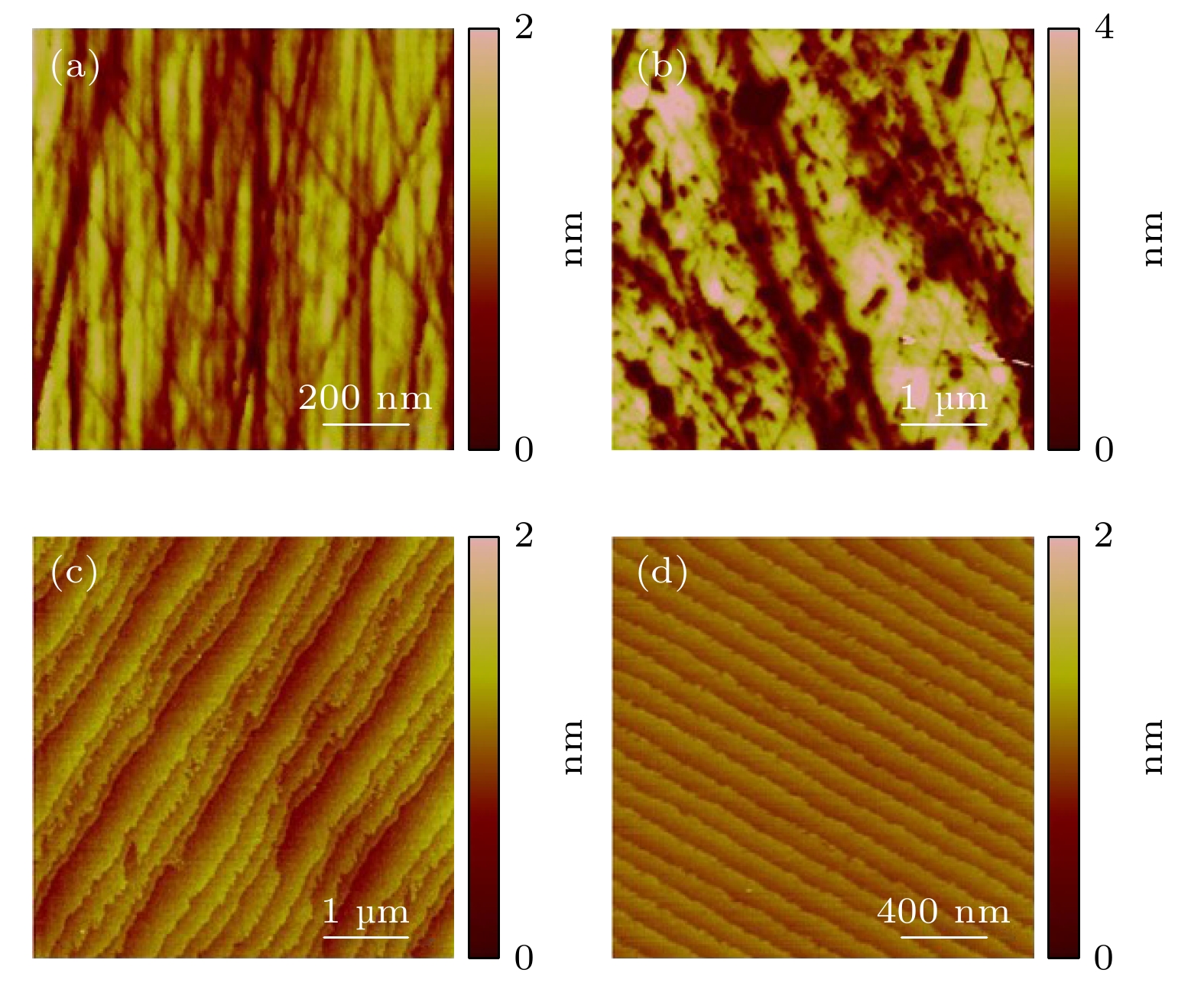
图 7 CMP加工SiC的AFM图(PV表示最高和最低处的差值; RMS是均方根)[45] (a) 金刚石抛光液(PV, 2.46 nm; RMS, 0.30 nm); (b) Al2O3抛光液(PV, 30.63 nm; RMS, 1.28 nm); (c) SiO2抛光液(PV, 2.01 nm; RMS, 0.15 nm); (d) CeO2抛光液(PV, 0.68 nm; RMS, 0.08 nm)
Fig. 7. AFM images of CMP-processed SiC (PV, peak to valley; RMS, root mean square)[45]: (a) Diamond slurry (PV, 2.46 nm; RMS, 0.30 nm); (b) Al2O3 slurry (PV, 30.63 nm; RMS, 1.28 nm); (c) SiO2 slurry (PV, 2.01 nm; RMS, 0.15 nm); (d) CeO2 slurry (PV, 0.68 nm; RMS, 0.08 nm).
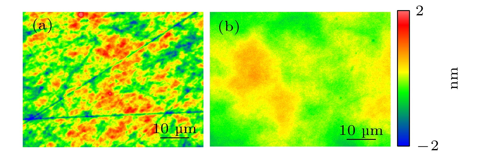
图 8 加工后4H-SiC的WLI测量结果[40] (a)不使用等离子体改性, 而仅以CeO2抛光后表面(PV, 5.49 nm; RMS, 0.57 nm); (b) PAP技术加工后表面(PV, 1.89 nm; RMS, 0.28 nm)
Fig. 8. WLI images of processed 4H-SiC wafer[40]: (a) The surface polished by ceria abrasive without plasma irradiation (PV, 5.49 nm; RMS, 0.57 nm); (b) the surface processed by PAP (PV, 1.89 nm; RMS, 0.28 nm).
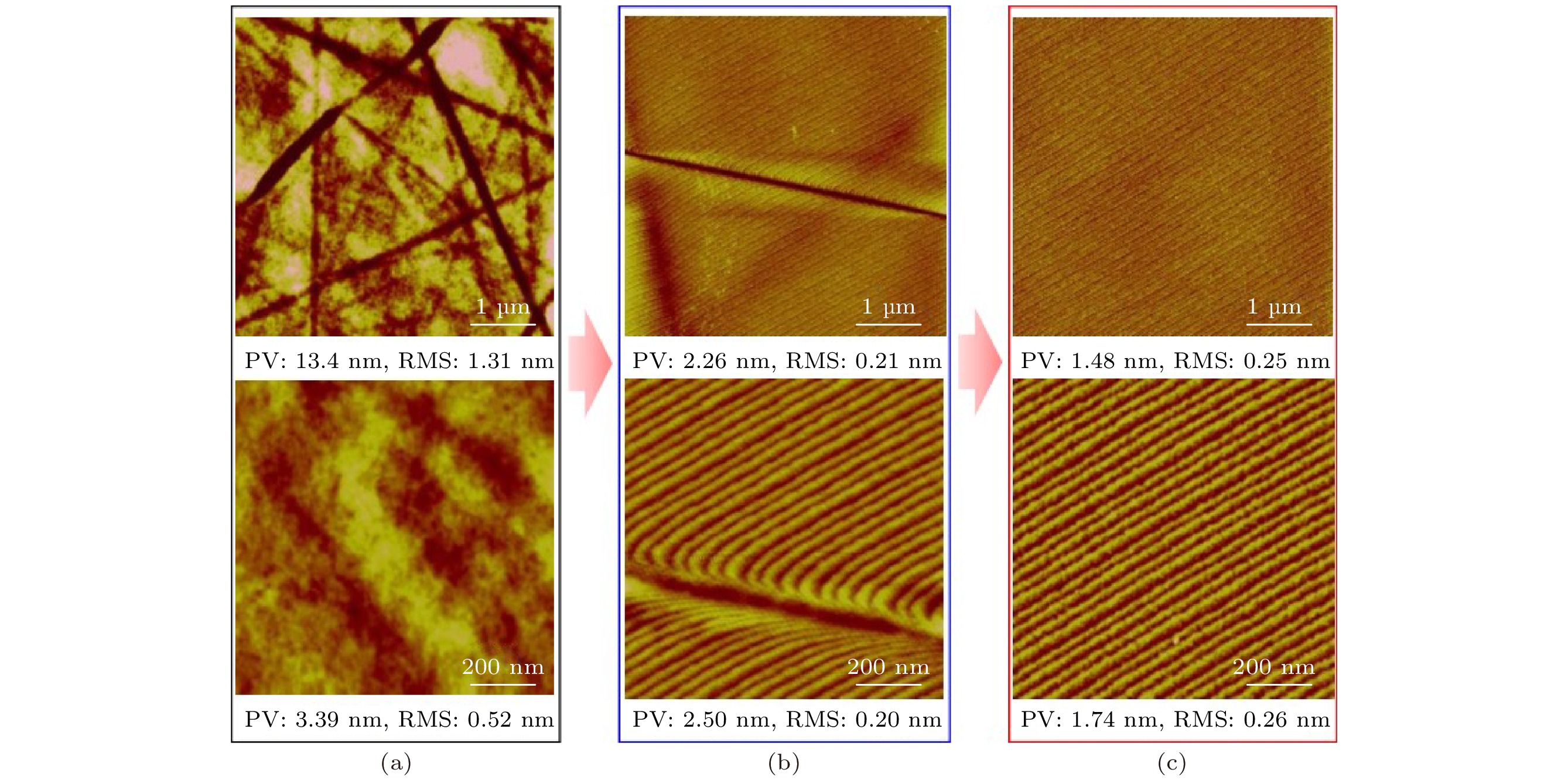

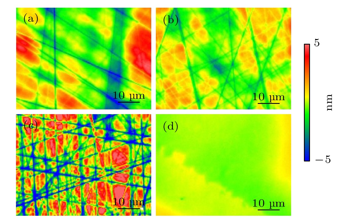
图 12 多次进行等离子体辐照和HF浸泡后的4H-SiC表面WLI图[48] (a)金刚石磨料抛光获得的初始表面(PV, 11.14 nm; RMS, 1.80 nm); (b)第一次处理后的结果(PV, 6.65 nm; RMS, 1.02 nm); (c)第二次处理后的结果(PV, 8.39 nm; RMS, 2.83 nm); (d)第三次处理后的结果(PV, 2.45 nm; RMS, 0.45 nm)
Fig. 12. WLI images of processed 4H-SiC surfaces[48]: (a) Diamond lapped surface (PV, 11.14 nm; RMS, 1.80 nm); (b) after the first cycle of plasma oxidation and HF dipping (PV, 6.65 nm; RMS, 1.02 nm); (c) after the second cycle (PV, 8.39 nm; RMS, 2.83 nm); (d) after the third cycle (PV, 2.45 nm; RMS, 0.45 nm).


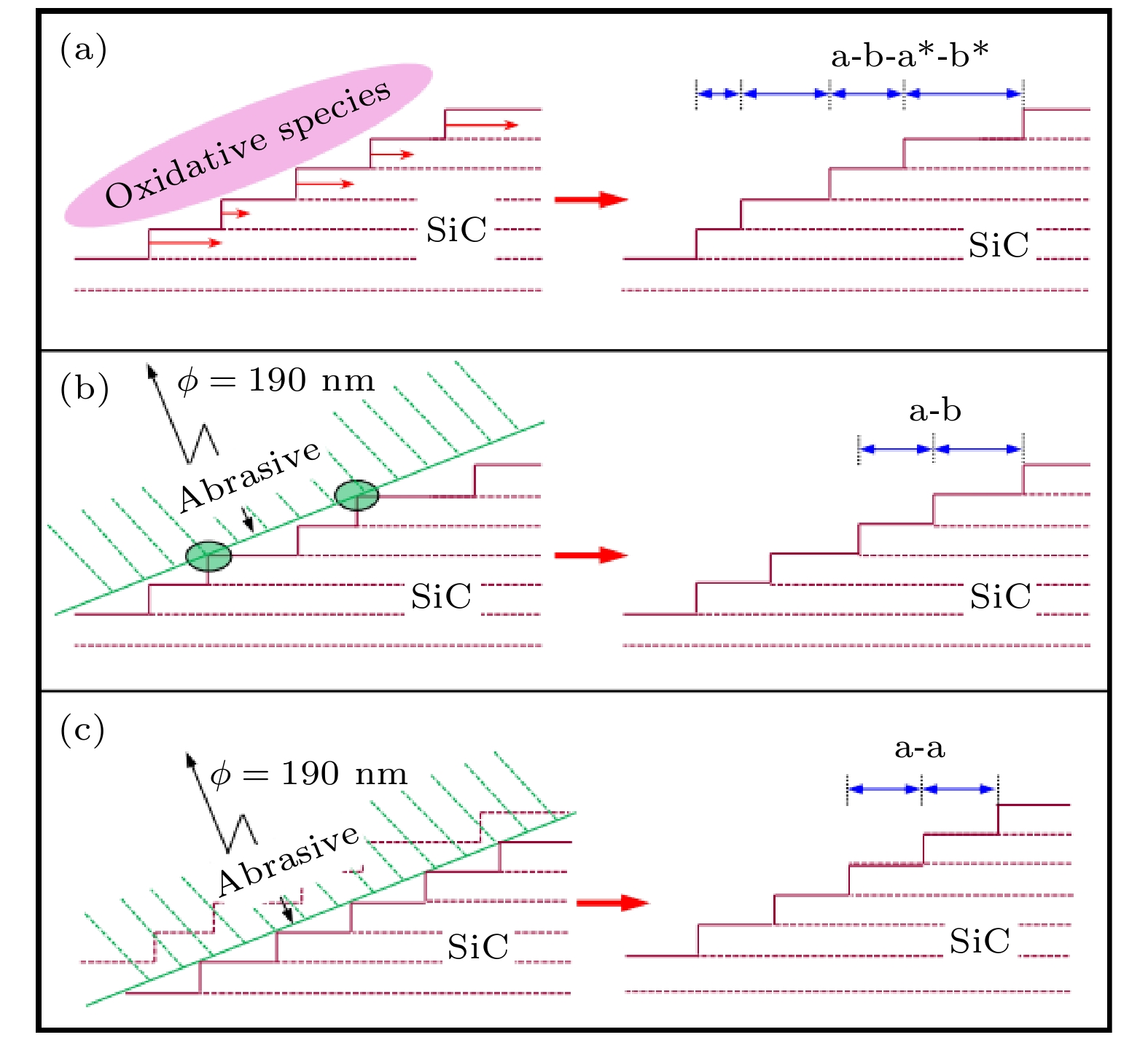
图 16 4H-SiC台阶状结构形成机制[65] (a)化学改性占主导机制, 产生a-b-a*-b*型结构; (b)化学改性作用与磨粒物理去除作用相当, 产生a-b型结构; (c)磨粒物理去除作用占主导机制, 形成a-a型结构
Fig. 16. Probable formation mechanism of step-terrace structure of 4H-SiC[65]: (a) Surface modification was dominant, resulting in the formation of the a-b-a*-b* type step-terrace structure; (b) physical removal was comparable with surface modification, resulting in the formation of the a-b type step-terrace structure; (c) physical removal was dominant, resulting in the formation of the a-a type step-terrace structure.
-
[1] Bencherif H, Pezzimenti F, Dehimi L, Della C 2020 Appl. Phys. A 126 854
Google Scholar
[2] Haddud A, Desouza A, Khare A, Lee H 2017 J. Manuf. Technol. Mana. 28 1055
Google Scholar
[3] He Y, Clark G, Schaibley J, He Y, Chen M, Wei Y, Ding X, Zhang Q, Yao W, Xu X, Lu C, Pan J 2015 Nat. Nanotechnol. 10 497
Google Scholar
[4] Mohammed M 2020 Plasmonics 15 1989
Google Scholar
[5] Kim S, Ahn H, Lim J, Lee K 2019 J. Korean Phys. Soc. 74 196
Google Scholar
[6] Kimura M, Koga Y, Nakanishi H, Matsuda T, Kameda T, Nakashima Y 2017 IEEE J. Electron Devi. 6 100
Google Scholar
[7] Zhang Q, Cheng L, Boutaba R 2010 J. Internet. Serv. Appl. 1 7
Google Scholar
[8] Umezawa H, Nagase M, Kato Y, Shikata S 2012 Diam. Relat. Mater. 24 201
Google Scholar
[9] Sharofidinov S, Kukushkin S, Redkov A, Grashchenko A, Osipov A 2019 Tech. Phys. Lett. 45 711
Google Scholar
[10] Domnich V, Aratyn Y, Kriven W, Gogotsi Y 2008 Rev. Adv. Mater. Sci. 17 33
[11] Qian J, Voronin G, Zerda T, He D, Zhao Y 2002 J. Mater. Res. 17 2153
Google Scholar
[12] Casady J, Johnson R 1996 Solid State Electron. 39 1409
Google Scholar
[13] Luo Q, Lu J, Xu X 2016 Wear 350/351 99
Google Scholar
[14] Li N, Ding J, Xuan Z, Huang J, Lin Z 2018 Strength Mater. 50 419
Google Scholar
[15] Dai S, Lei H, Fu J 2020 J. Electron. Mater. 49 1301
Google Scholar
[16] Heydemann V, Everson W, Gamble R, Snyder D, Skowronski M 2004 Mater. Sci. Forum 457/460 805
Google Scholar
[17] Zhou L, Audurier V, Pirouz P, Powell J 1997 J. Electrochem. Soc. 144 161
Google Scholar
[18] Pan G, Zhou Y, Luo G, Shi X, Zou C, Gong H 2013 J. Mater. Sci. Mater. Electron. 24 5040
Google Scholar
[19] Kato T, Wada K, Hozomi E, Taniguchi H, Miura T, Nishizawa S, Arai K 2007 Mater. Sci. Forum 556/557 753
Google Scholar
[20] Neslen C, Mitchel W, Hengehold R 2001 J. Electron. Mater. 30 1271
Google Scholar
[21] Lee H, Kim M, Jeong H 2015 Int. J. Precis. Eng. Manuf. 16 2611
Google Scholar
[22] Lee H, Kim D, An J, Lee H, Kim K, Jeong H 2010 CIRP Ann. Manuf. Techn. 59 333
[23] Kurokawa S, Doi T, Wang C, Sano Y, Aida H, Oyama K, Takahashi K 2014 ECS Trans. 60 641
Google Scholar
[24] Zhou Y, Pan G S, Shi X L, Gong H, Luo G H, Gu Z H 2014 Surf. Coat. Tech. 251 48
Google Scholar
[25] Shi X L, Pan G S, Zhou Y, Gu Z H, Gong H, Zou C L 2014 Appl. Surf. Sci. 307 414
Google Scholar
[26] Liang H, Yan Q, Lu J, Luo B, Xiao X 2019 Int. J. Adv. Manuf. Tech. 103 1337
Google Scholar
[27] Zhai W J, Gao B, Chang J, Wang H 2019 Nanomanuf. Metrol. 2 36
Google Scholar
[28] 路家斌, 熊强, 阎秋生, 王鑫, 廖博涛 2019 表面技术 48 148
Lu J B, Xiong Q, Yan Q S, Wang X, Liao B T 2019 Surf. Tech. 48 148
[29] Murata J, Yodogawa K, Ban K 2017 Int. J. Mach. Tool. Manu. 114 1
[30] Shen X, Tu Q, Deng H, Jiang G, He X, Liu B, Yamamura K 2016 Appl. Phys. A 122 354
Google Scholar
[31] Deng H, Hosoya K, Imanishi Y, Endo K, Yamamura K 2015 Electrochem. Commun. 52 5
Google Scholar
[32] Kubota A, Yoshimura M, Fukuyama S, Iwamoto C, Touge M 2012 Precis. Eng. 36 137
Google Scholar
[33] Kubota A, Yagi K, Murata J, Yasui H, Miyamoto S, Hara H, Sano Y, Yamauchi K 2009 J. Electron. Mater. 38 159
Google Scholar
[34] Zhang P, Feng X, Yang J 2014 J. Semicond. 35 166
[35] Nitta H, Isobe A, Hong P, Hirao T 2011 Jpn. J. Appl. Phys. 50 046501
Google Scholar
[36] Kubota A, Fukuyama S, Ichimori Y, Touge M 2012 Diam. Relat. Mater. 24 59
Google Scholar
[37] Ballarin N, Carraro C, Maboudian R, Magagnin L 2014 Electrochem. Commun. 40 17
Google Scholar
[38] Lin Y, Kao C 2005 Int. J. Adv. Manuf. Tech. 25 33
Google Scholar
[39] Yamamura K, Takiguchi T, Ueda M, Hattori A, Zettsu N 2010 Adv. Mat. Res. 126-128 423
Google Scholar
[40] Yamamura K, Takiguchi T, Ueda M, Deng H, Hattori A, Zettsu N 2011 CIRP Ann. Manuf. Techn. 60 571
Google Scholar
[41] Mori Y, Yamamura K, Sano Y 2004 Rev. Sci. Instrum. 75 942
Google Scholar
[42] Sano Y, Yamamura K, Mimura H, Yamauchi K, Mori Y 2007 Rev. Sci. Instrum. 78 086102
Google Scholar
[43] Yamamura K, Ueda K, Nagano M, Zettsu N, Maeo S, Shimada S, Utaka T, Taniguchi K 2010 Nucl. Instrum. Meth. A 616 281
Google Scholar
[44] Sun R, Yang X, Watanabe K, Miyazaki S, Fukano T, Kitada M, Arima K, Kawai K, Yamamura K 2019 Nanomanuf. Metrol. 2 168
Google Scholar
[45] Deng H 2016 Ph. D. Dissertation (Osaka: Osaka University)
[46] Harb T, Kedzierski W, McConkey J 2001 J. Chem. Phys. 115 5507
Google Scholar
[47] Krstulovic N, Labazan I, Milosevic S, Cvelbar U, Vesel A, Mozetic M 2006 J. Phys. D: Appl. Phys. 39 3799
Google Scholar
[48] Deng H, Yamamura K 2013 CIRP Ann. Manuf. Techn. 62 575
Google Scholar
[49] Deng H, Ueda M, Yamamura K 2014 Int. J. Adv. Manuf. Tech. 72 1
[50] 张海霞, 张泰华, 郇勇 2003 微纳电子技术 40 245
Google Scholar
Zhang H X, Zhang T H, Huan Y 2003 Micronanoelectron. Tech. 40 245
Google Scholar
[51] Ashida K, Dojima D, Kutsuma Y, Torimi S, Nogami S, Imai Y, Kimura S, Mizuki J, Ohtani N, Kaneko T 2016 MRS Advances 1 3697
Google Scholar
[52] Lakhdari F, Belkhir N, Bouzid D, Herold V 2019 Int. J. Adv. Manuf. Tech. 102 1421
Google Scholar
[53] Deng H, Takiguchi T, Ueda M, Hattori1 A, Zettsu N, Yamamura K 2011 Jpn. J. Appl. Phys. 50 08JG05
[54] Palmieri R, Radtke C, Boudinov H, Silva E 2009 Appl. Phys. Lett. 95 113504
Google Scholar
[55] Shi X, Pan G, Zhou Y, Zou C, Gong H 2013 Appl. Surf. Sci. 284 195
Google Scholar
[56] Shi X, Pan G, Zhou Y, Xu L, Zou C, Gong H 2015 Surf. Coat. Tech. 270 206
Google Scholar
[57] Okamoto T, Sano Y, Tachibana K, Arima K, Hattori A, Yagi K, Murata J, Sadakuni S, Yamauchiet K 2011 J. Nanosci. Nanotechno. 11 2928
Google Scholar
[58] Hara H, Sano Y, Mimura H, Arima K, Kubota A, Yagi K, Murata J, Yamauchi K 2006 J. Electron. Mater. 35 11
Google Scholar
[59] Kubota A, Mimura H, Inagaki K, Arima K, Mori Y, Yamauchi K 2005 J. Electron. Mater. 34 439
Google Scholar
[60] Okamoto T, Sano Y, Hara H, Mimura H, Arima K, Yagi K, Murata J, Yamauchi K 2009 Mater. Sci. Forum 600-603 835
[61] Okamoto T, Sano Y, Hara H, Hatayama T, Arima K, Yagi K, Murata J, Sadakuni S, Tachibana K, Shirasawa Y, Mimura H, Fuyuki T, Yamauchi K 2010 Mater. Sci. Forum 645-648 775
[62] Deng H, Endo K, Yamamura K 2013 Appl. Phys. Lett. 103 111603
Google Scholar
[63] Deng H, Endo K, Yamamura K 2014 Appl. Phys. Lett. 104 101608
Google Scholar
[64] Deng H, Monna K, Tabata T, Endo K, Yamamura K 2014 CIRP Ann. Manuf. Techn. 63 529
Google Scholar
[65] Deng H, Endo K, Yamamura K 2015 Sci. Rep. 5 8947
Google Scholar
[66] Rokicki R, Hryniewicz R 2012 T. I. Met. Finish. 90 188
Google Scholar
[67] Suratwala T, Steele W, Wong L, Feit M, Miller P, Spears R, Shen N, Desjardin R 2015 J. Am. Ceram. Soc. 98 2395
Google Scholar
[68] Shaw J, Heine V 1990 J. Phys. Condens. Mater. 2 4351
Google Scholar
[69] Chien F, Nutt S, Yoo W, Kimoto K, Matsunami H 1994 J. Mater. Res. 9 940
Google Scholar
[70] Kimoto T, Itoh A, Matsunami H, Okano T 1997 J. Appl. Phys. 81 3494
Google Scholar
[71] Heine V, Cheng C, Needs R 1991 J. Am. Ceram. Soc. 74 2630
Google Scholar
[72] Yazdi G, Vasiliauskas R, Iakimov T, Zakharov A, Syvajarvi M, Yakimova R 2013 Carbon 57 477
Google Scholar
[73] Arima K, Hara H, Murata J, Ishida T, Okamoto R, Yagi K, Sano Y, Mimura H, Yamauchi K 2007 Appl. Phys. Lett. 90 202106
Google Scholar
[74] Hoshino T, Kurata Y, Terasaki Y, Susa K 2001 J. Non-Cryst. Solids 283 129
Google Scholar
[75] Oh M, Singh R, Gupta S, Cho S 2010 Microelectron. Eng. 87 2633
Google Scholar
[76] Zho L, Eda H, Shimizu J, Kamiya S, Iwase H, Kimura S 2006 CIRP Ann. Manuf. Techn. 55 313
Google Scholar
[77] Tian Y, Zhou L, Shimizu J, Tashiro Y, Kang R 2009 Appl. Surf. Sci. 255 4205
Google Scholar
[78] Kamiya S, Iwase H, Kishita K, Zhou L, Eda H, Yoshida Y 2009 J. Vac. Sci. Technol. B 27 1496
Google Scholar
[79] Deng H, Endo K, Yamamura K 2015 Appl. Phys. Lett. 107 051602
Google Scholar
[80] Deng H, Endo K, Yamamura K 2015 CIRP Ann. Manuf. Techn. 64 531
Google Scholar
[81] Yamamura K, Emori K, Sun R, Ohkubo Y, Endo K, Yamada H, Chayahara A, Mokuno Y 2018 CIRP Ann. Manuf. Techn. 67 353
Google Scholar
[82] Deng H, Endo K, Yamamura K 2017 Int. J. Mach. Tool. Manu. 115 38
Google Scholar
[83] Deng H, Yamamura K 2012 Curr. Appl. Phys. 12 S24
[84] Shen X, Dai Y, Deng H, Guan C, Yamamura K 2013 Opt. Express 21 26123
Google Scholar
[85] Shen X, Tu Q, Deng H, Jiang G, Yamamura K 2015 Opt. Eng. 54 055106
Google Scholar
[86] Fang F 2020 Int. J. Extrem. Manuf. 2 030201
Google Scholar


 下载:
下载:

计量
- 文章访问数: 16925
- PDF下载量: 587
- 被引次数: 0
