


-
The electrical performance and the long-term reliability of GaN-based high electron mobility transistors (HEMTs) are greatly affected by the Joule self-heating effect under high power density operation condition. Measurement of the junction temperature and analysis of the thermal resistance of the constituent layers including the packaging material are critically important for thermal design and reliability assessment of GaN-based HEMTs. In this paper, Raman thermometry combined with the finite element thermal simulation is used to compare the junction temperature and the thermal resistance of a GaN HEMT mounted on a novel Cu/graphite composite flange with those of a conventional CuMo flanged device. The results show that the junction temperature of the Cu/graphite flanged device is 15% lower than that of the CuMo flanged device at a power dissipation of 1.43 W/mm, while the overall device thermal resistance is 18.7% lower in the Cu/graphite flanged device. In addition, the temperature distributions of each layer along the cross-plane direction are analyzed for the two devices; the thermal resistance ratio of the Cu/graphite flange is 40% of the overall device thermal resistance, while the CuMo flange account for 53% of the overall thermal resistance of the device. This proves the effectiveness and benefit of using the Cu/graphite composite material package of high thermal conductivity to improve the heat dissipation of GaN HEMTs. By tuning the mass fraction of the graphite, it is possible to further increase the thermal conductivity of the Cu/graphite composite flange and to further reduce the device thermal resistance. It is observed in the Raman thermal measurement that the highest thermal resistance after flanging is the interfacial thermal resistance between the GaN epitaxial layer and the SiC substrate (~50 m2·K/GW). For obtaining the better thermal characteristics of the GaN HEMT, it is crucial to reduce the GaN/SiC interfacial thermal resistance through interface engineering during the epitaxial growth. In the meantime, Raman thermometry combined with the finite element thermal simulation is demonstrated to be an effective method for implementing the thermal characterization of the GaN-based devices and the constituent material layers, and the principle and procedure of the method are described in detail in the paper.
-
Keywords:
- GaN high electron mobility transistor /
- thermal resistance /
- Cu/graphite flange /
- Raman thermometry
[1] Huang H, Sun Z, Cao Y, Li F, Zhang F, Wen Z, Hu L 2018 J. Phys. D: Appl. Phys. 51 345102
 Google Scholar
[2] Huang H, Li F, Sun Z, Cao Y 2018 Micromachines 9 658
Google Scholar
[3] Bagnall K R, Saadat O I, Joglekar S, Palacios T, Wang E N 2017 IEEE Trans. Electron Devices. 64 2121
Google Scholar
[4] Chen K J, Häberlen O, Lidow A, Tsai C L, Ueda T, Uemoto Y, Wu Y 2017 IEEE Trans. Electron Devices. 64 779
Google Scholar
[5] 张志荣, 房玉龙, 尹甲运, 郭艳敏, 王波, 王元刚, 李佳, 芦伟立, 高楠, 刘沛, 冯志红 2018 物理学报 67 076801
Google Scholar
Zhang Z R, Fang Y L, Yin J Y, Guo Y M, Wang B, Wang Y G, Li J, Lu W L, Gao N, Liu P, Feng Z H 2018 Acta Phys. Sin. 67 076801
Google Scholar
[6] 唐文昕, 郝荣晖, 陈扶, 于国浩, 张宝顺 2018 物理学报 67 198501
Google Scholar
Tang W X, Hao R H, Chen F, Yu G H, Zhang B S 2018 Acta Phys. Sin. 67 198501
Google Scholar
[7] Wu Y F, Moore M, Saxler A, Wisleder T, Parikh P 2006 64th Device Research Conference IEEE State College, PA, USA, June 26–28, 2006 p151
[8] Zhou Y, Anaya J, Pomeroy J, Sun H, Gu X, Xie A, Kuball M 2017 ACS Appl. Mater. Interfaces 9 34416
Google Scholar
[9] Sun H R, Pomeroy J W, Simon R B, Francis D, Faili F, Twitchen D J, Kuball M 2016 IEEE Electron Device Lett. 37 621
Google Scholar
[10] Won Y, Cho J, Agonafer D, Asheghi M, Goodson K E 2015 IEEE Trans. Compon., Packag., Manuf. Technol. 5 737
Google Scholar
[11] Sun H R, Simon R B, Pomeroy J W, Francis D, Faili F, Twitchen D J, Kuball M 2015 Appl. Phys. Lett. 106 111906
Google Scholar
[12] Yan Z, Liu G, Khan J M, Balandin A A 2012 Nat. Commun. 3 827
Google Scholar
[13] Ma Z H, Cao H C, Lin S, Li X D, Zhao L X 2019 Solid-State Electron. 156 92
Google Scholar
[14] Manoi A, Pomeroy J W, Killat N, Kuball M 2010 IEEE Electron Device Lett. 31 1395
Google Scholar
[15] 张昊明, 何新波, 沈晓宇, 刘谦, 曲选辉 2012 粉末冶金材料科学与工程 17 339
Google Scholar
Zhang Y M, He X B, Shen X Y, Liu Q, Qu X H 2012 Mater. Sci. Eng. Powder. Metall. 17 339
Google Scholar
[16] 许尧, 薛鹏举, 魏青松, 史玉生 2013 热加工工艺 42 111
Xu Y, Xue P J, Wei Q S, Shi Y S 2013 Hot Working Technol. 42 111 (in Chinese)
[17] Fu J J, Zhao L X, Cao H C, Sun X J, Sun B J, Wang J X, Li J M 2016 AIP Adv. 6 055219
Google Scholar
[18] Kuball M, Pomeroy J W 2016 IEEE Trans. Device Mater. Reliab. 16 667
Google Scholar
[19] Pomeroy J W, Bernardoni M, Dumka D C, Fanning D M, Kuball M 2014 Appl. Phys. Lett. 104 083513
Google Scholar
[20] Anaya J, Rossi S, Alomari M, Kohn E, Tóth L, Pécz B, Kuball M 2015 Appl. Phys. Lett. 106 223101
Google Scholar
[21] Pomeroy J W, Middleton C, Singh M, Dalcanale S, Uren M J, Wong M H, Kuball M 2018 IEEE Electron Device Lett. 40 189
[22] Sarua A, Ji H, Kuball M, Uren M J, Martin T, Hilton K P, Balmer R S 2006 IEEE Trans. Electron Devices. 53 2438
Google Scholar
[23] Wang A, Tadjer M J, Calle F 2013 Semicond. Sci. Technol. 28 055010
Google Scholar
[24] Guo H, Kong Y, Chen T 2017 Diamond Relat. Mater. 73 260
Google Scholar
[25] Zou B, Sun H R, Guo H X, Dai B, Zhu J Q 2019 Diamond Relat. Mater. 95 28
Google Scholar
[26] Riedel G J, Pomeroy J W, Hilton K P, Maclean J O, Wallis D J, Uren M J, Pozina G 2008 IEEE Electron Device Lett. 30 103
[27] Liu K, Zhao J W, Sun H R, Guo H X, Dai B, Zhu J Q 2019 Chin. Phys. B 28 060701
Google Scholar
-

图 1 (a)被测GaN高电子迁移率场效应管器件结构以及拉曼热测量的示意图; (b)被测器件在50 ℃和300 ℃的拉曼特征峰: 包括GaN外延的E2(high)和A1(LO)峰, 以及SiC衬底的FTO峰
Figure 1. (a) Schematic structure of the GaN-on-SiC HEMT under test in the Raman optothermal measurement; (b) Raman peaks of the GaN-on-SiC HEMT at 50 ℃ and 300 ℃, including the E2(high) and A1(LO) peaks of the GaN epitaxy and the FTO peak of the SiC substrate.
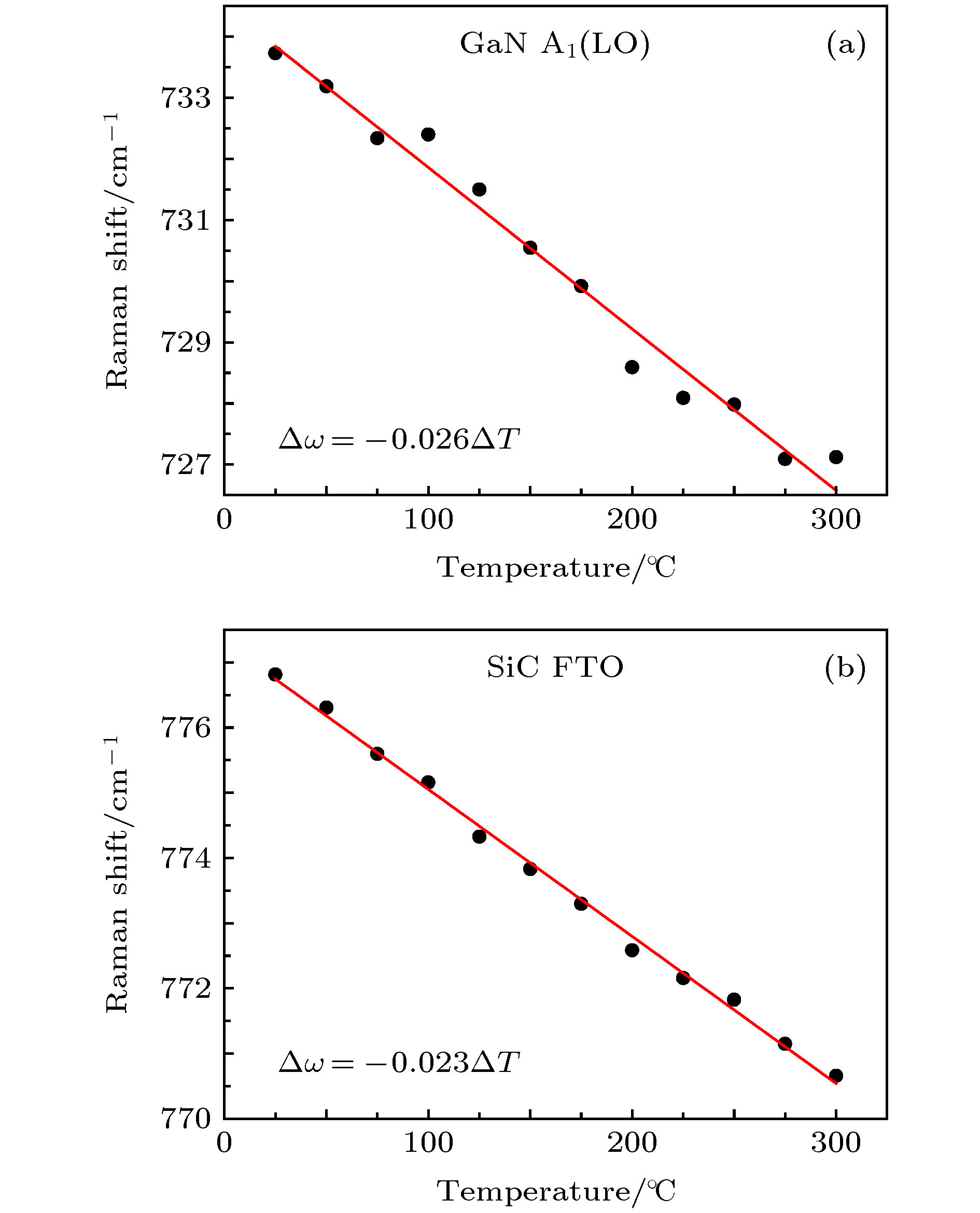
图 2 (a) GaN A1(LO)拉曼峰随温度的变化关系, 线性拟合得到的温度系数为–0.026 cm–1·K–1; (b) SiC FTO拉曼峰随温度的变化关系, 线性拟合得到的温度系数为–0.023 cm–1·K–1
Figure 2. (a) Position of the GaN A1(LO) Raman peak as a function of temperature. The temperature coefficient from the linear fit is –0.026 cm–1·K–1; (b) position of the SiC FTO Raman peak as a function of temperature. The temperature coefficient from the linear fit is –0.023 cm–1·K–1.
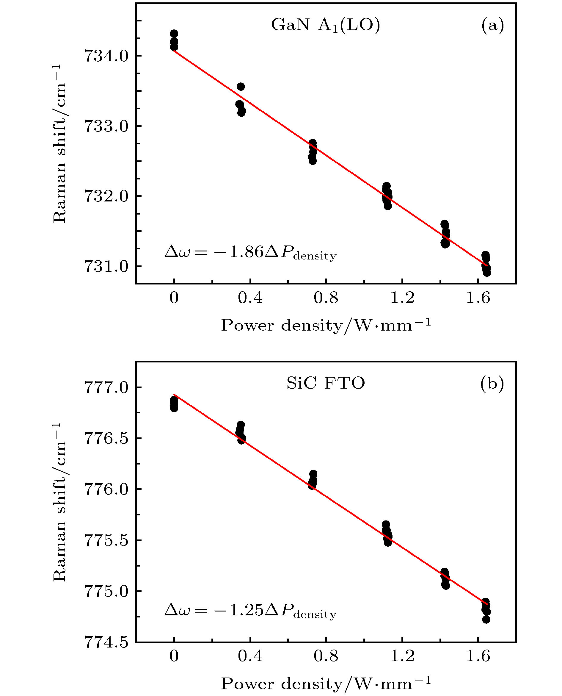
图 3 (a) GaN A1(LO)拉曼峰随器件功率密度的变化关系, 线性拟合得到的功率系数为–1.86 cm–1·mm/W; (b) SiC FTO拉曼峰随器件功率密度的变化关系, 线性拟合得到的功率系数为–1.25 cm–1·mm/W的功率系数
Figure 3. (a) Position of the GaN A1(LO) Raman peak as a function of the device power density. The power density coefficient from the linear fit is –1.86 cm–1·mm/W; (b) position of the SiC FTO Raman peak as a function of the device power density. The power density coefficient from the linear fit is –1.25 cm–1·mm/W.
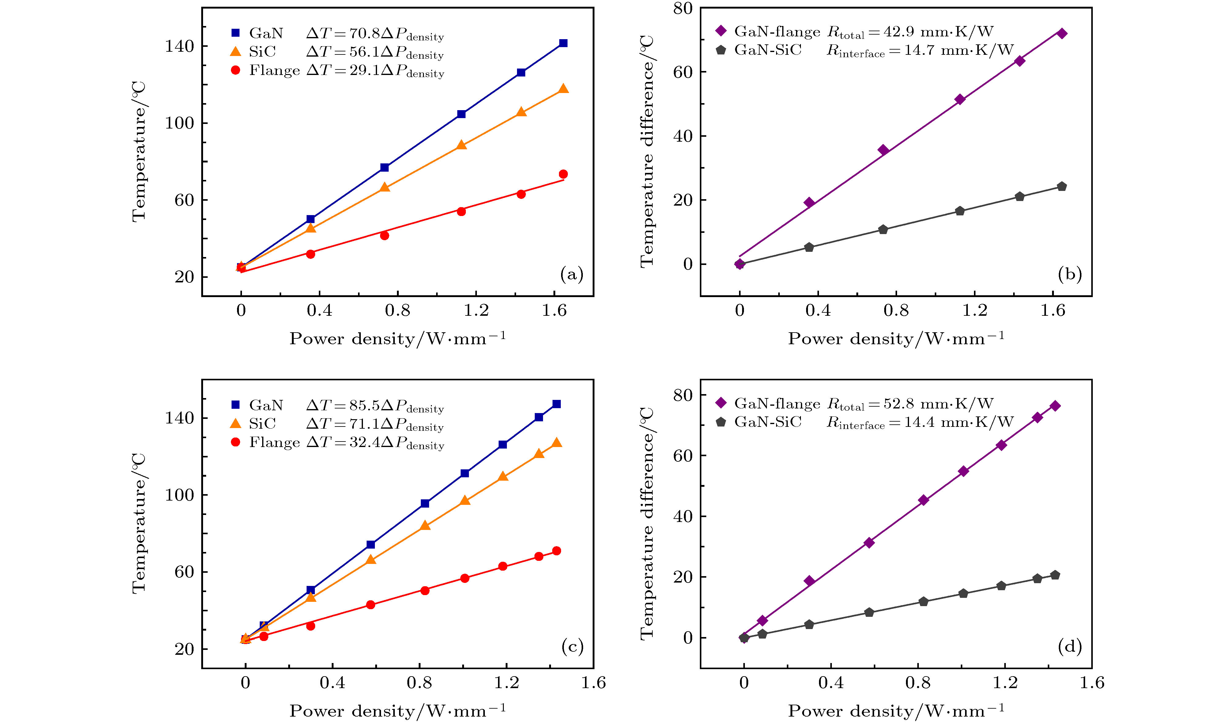
图 4 (a)铜/石墨法兰封装器件GaN层、SiC上表层和封装法兰的温度随功率密度的变化; (b)铜/石墨法兰封装器件GaN层和SiC上表层的温度差、GaN层和封装法兰之间的温度差随功率密度的变化; (c)铜钼法兰封装器件GaN层、SiC上表层和封装法兰的温度随功率密度的变化; (d)铜钼法兰封装器件GaN层和SiC上表层的温度差、GaN层和封装法兰之间的温度差随功率密度增加的变化
Figure 4. (a) Measured temperature of GaN, SiC, and the Cu/graphite flange as a function of the device power density; (b) temperature differences between GaN and SiC, and between GaN and and the Cu/graphite flange as a function of the device power density; (c) measured temperature of GaN, SiC, and the CuMo flange as a function of the device power density; (b) temperature differences between GaN and SiC, and between GaN and and the CuMo flange as a function of the device power density.
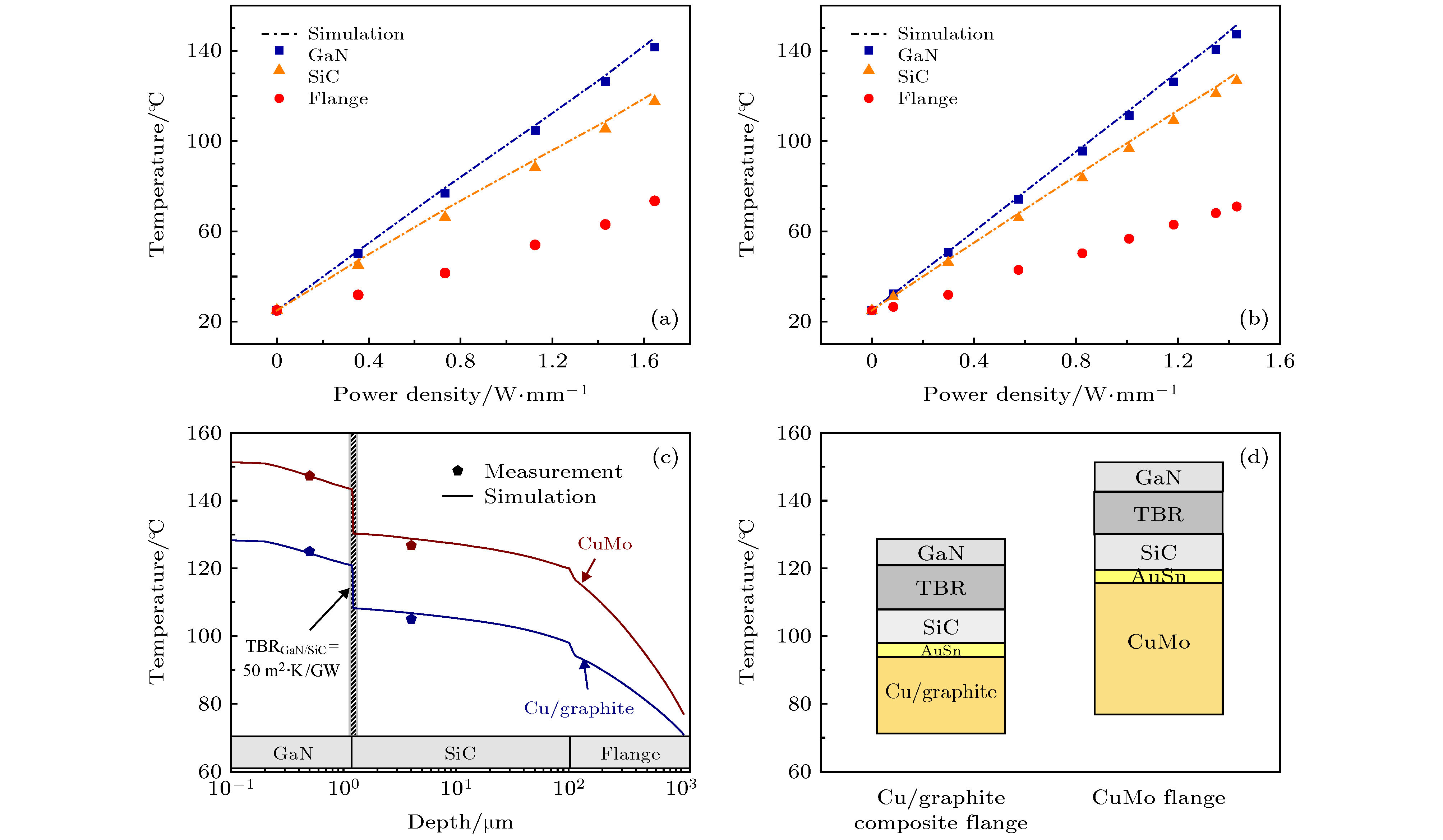
图 5 (a)铜/石墨法兰封装的GaN器件的GaN外延和SiC衬底上表层温度的模拟值(线)和实测值(点); (b)铜钼法兰GaN电子器件的结温和SiC衬底上表层温度的模拟值和实测值的对比; (c) 1.43 W/mm功率密度下铜/石墨法兰和铜钼法兰封装GaN器件在垂直器件表面方向上的温度分布; (d)铜/石墨法兰和铜钼法兰封装GaN器件各层材的热阻占比(其中TBR的材料为AlN)
Figure 5. (a) Simulated (line) and measured (dot) junction temperatures of the Cu/graphite flanged device; (b) simulated (line) and measured (dot) junction temperatures of the CuMo flanged device; (c) depth wise temperature distribution of the Cu/graphite flanged device and the CuMo flanged device at the power density of 1.43 W/mm; (d) thermal resistance of each layer within the Cu/graphite flanged device and the CuMo flanged device (The material of TBR is AlN).
表 1 两种铜基法兰封装GaN器件的热阻对比
Table 1. Thermal resistance of GaN HEMT with different Cu-based flange materials.
GaN场效应管法兰封装材料 热导率/W·(m·K)–1 GaN-SiC间热阻/mm·K·W–1 器件整体热阻/mm·K·W–1 铜/石墨 300 14.7 42.9 铜钼 167 14.4 52.8  DownLoad: CSV
表 2 有限元热仿真分析中使用的各层材料的尺寸及热导率
Table 2. Dimensions and thermal conductivity of each layer in the GaN-on-SiC HEMT used in the finite element device thermal simulation.
DownLoad: CSV
-
[1] Huang H, Sun Z, Cao Y, Li F, Zhang F, Wen Z, Hu L 2018 J. Phys. D: Appl. Phys. 51 345102
Google Scholar
[2] Huang H, Li F, Sun Z, Cao Y 2018 Micromachines 9 658
Google Scholar
[3] Bagnall K R, Saadat O I, Joglekar S, Palacios T, Wang E N 2017 IEEE Trans. Electron Devices. 64 2121
Google Scholar
[4] Chen K J, Häberlen O, Lidow A, Tsai C L, Ueda T, Uemoto Y, Wu Y 2017 IEEE Trans. Electron Devices. 64 779
Google Scholar
[5] 张志荣, 房玉龙, 尹甲运, 郭艳敏, 王波, 王元刚, 李佳, 芦伟立, 高楠, 刘沛, 冯志红 2018 物理学报 67 076801
Google Scholar
Zhang Z R, Fang Y L, Yin J Y, Guo Y M, Wang B, Wang Y G, Li J, Lu W L, Gao N, Liu P, Feng Z H 2018 Acta Phys. Sin. 67 076801
Google Scholar
[6] 唐文昕, 郝荣晖, 陈扶, 于国浩, 张宝顺 2018 物理学报 67 198501
Google Scholar
Tang W X, Hao R H, Chen F, Yu G H, Zhang B S 2018 Acta Phys. Sin. 67 198501
Google Scholar
[7] Wu Y F, Moore M, Saxler A, Wisleder T, Parikh P 2006 64th Device Research Conference IEEE State College, PA, USA, June 26–28, 2006 p151
[8] Zhou Y, Anaya J, Pomeroy J, Sun H, Gu X, Xie A, Kuball M 2017 ACS Appl. Mater. Interfaces 9 34416
Google Scholar
[9] Sun H R, Pomeroy J W, Simon R B, Francis D, Faili F, Twitchen D J, Kuball M 2016 IEEE Electron Device Lett. 37 621
Google Scholar
[10] Won Y, Cho J, Agonafer D, Asheghi M, Goodson K E 2015 IEEE Trans. Compon., Packag., Manuf. Technol. 5 737
Google Scholar
[11] Sun H R, Simon R B, Pomeroy J W, Francis D, Faili F, Twitchen D J, Kuball M 2015 Appl. Phys. Lett. 106 111906
Google Scholar
[12] Yan Z, Liu G, Khan J M, Balandin A A 2012 Nat. Commun. 3 827
Google Scholar
[13] Ma Z H, Cao H C, Lin S, Li X D, Zhao L X 2019 Solid-State Electron. 156 92
Google Scholar
[14] Manoi A, Pomeroy J W, Killat N, Kuball M 2010 IEEE Electron Device Lett. 31 1395
Google Scholar
[15] 张昊明, 何新波, 沈晓宇, 刘谦, 曲选辉 2012 粉末冶金材料科学与工程 17 339
Google Scholar
Zhang Y M, He X B, Shen X Y, Liu Q, Qu X H 2012 Mater. Sci. Eng. Powder. Metall. 17 339
Google Scholar
[16] 许尧, 薛鹏举, 魏青松, 史玉生 2013 热加工工艺 42 111
Xu Y, Xue P J, Wei Q S, Shi Y S 2013 Hot Working Technol. 42 111 (in Chinese)
[17] Fu J J, Zhao L X, Cao H C, Sun X J, Sun B J, Wang J X, Li J M 2016 AIP Adv. 6 055219
Google Scholar
[18] Kuball M, Pomeroy J W 2016 IEEE Trans. Device Mater. Reliab. 16 667
Google Scholar
[19] Pomeroy J W, Bernardoni M, Dumka D C, Fanning D M, Kuball M 2014 Appl. Phys. Lett. 104 083513
Google Scholar
[20] Anaya J, Rossi S, Alomari M, Kohn E, Tóth L, Pécz B, Kuball M 2015 Appl. Phys. Lett. 106 223101
Google Scholar
[21] Pomeroy J W, Middleton C, Singh M, Dalcanale S, Uren M J, Wong M H, Kuball M 2018 IEEE Electron Device Lett. 40 189
[22] Sarua A, Ji H, Kuball M, Uren M J, Martin T, Hilton K P, Balmer R S 2006 IEEE Trans. Electron Devices. 53 2438
Google Scholar
[23] Wang A, Tadjer M J, Calle F 2013 Semicond. Sci. Technol. 28 055010
Google Scholar
[24] Guo H, Kong Y, Chen T 2017 Diamond Relat. Mater. 73 260
Google Scholar
[25] Zou B, Sun H R, Guo H X, Dai B, Zhu J Q 2019 Diamond Relat. Mater. 95 28
Google Scholar
[26] Riedel G J, Pomeroy J W, Hilton K P, Maclean J O, Wallis D J, Uren M J, Pozina G 2008 IEEE Electron Device Lett. 30 103
[27] Liu K, Zhao J W, Sun H R, Guo H X, Dai B, Zhu J Q 2019 Chin. Phys. B 28 060701
Google Scholar

 DownLoad:
Catalog
Metrics
- Abstract views: 7264
- PDF Downloads: 120
- Cited By: 0
