


-
采用181Ta32+重离子辐射AlGaN/GaN高电子迁移率晶体管, 获得器件在重离子辐射前后的电学特性和低频噪声特性. 重离子辐射导致器件的阈值电压正向漂移、最大饱和电流减小等电学参数的退化. 微光显微测试发现辐射后器件热点数量明显增加, 引入更多缺陷. 随着辐射注量的增加, 电流噪声功率谱密度逐渐增大, 在注量为1×10¹⁰ ions/cm2重离子辐射后, 缺陷密度增大到3.19×1018 cm–3·eV–1, 不同栅压下的Hooge参数增大. 通过漏极电流噪声归一化功率谱密度随偏置电压的变化分析, 发现重离子辐射产生的缺陷会导致寄生串联电阻增大.AlGaN/GaN high election mobility transistor (HEMT) has important application prospects in satellite communication, radar, nuclear reactors and other extreme environments, owing to its excellent electrical performance and strong radiation resistance. Heavy ion radiation mainly causes single-event effect and displacement damage effect in AlGaN/GaN HEMT device. In this work, the displacement damage defects introduced by heavy ion radiation are analyzed in detail. With the increase of heavy ion radiation influence, more defects are introduced by displacement damage. These defects reduce the two-dimensional electron gas (2DEG) concentration through carrier capture and removal effect, and reduce the carrier mobility through scattering mechanism, resulting in gradual degradation of the electrical characteristics of the device. In this work, AlGaN/GaN high electron mobility transistors are irradiated by 181Ta32+ ions with fluences of 1×10⁸ ions/cm2, 1×10⁹ ions/cm2 and 1×10¹⁰ ions/cm2. The electrical characteristics, EMMI and low-frequency noise characteristics of the device before and after heavy ion radiation are measured. The results show that heavy ion radiation can lead to the degradation of electrical parameters. When the heavy ion radiation dose reaches 1×10¹⁰ ions/cm2, the electrical characteristics of the device deteriorate seriously, the threshold voltage shifts forward by 25%, and the drain saturation current deteriorates obviously. The defect locations introduced by irradiation are analyzed by EMMI test, and it is found that the number of “hot spots” increases significantly after the having been irradiated by heavy ions with a fluence of 1×10¹⁰ ions/cm2, indicating that the radiation leads to the increase of defect density and serious damage to the device. Through the noise test, it is found that with the increase of the radiation fluence, the current noise power spectral density gradually increases. When the fluence reaches 1×10¹⁰ ions/cm2, the defect density increases to 3.19×1018 cm–3·eV–1, and the Hooge parameter increases after having been irradiated by heavy ions. We believe that the radiation leads to the defect density and parasitic series resistance of AlGaN/GaN HEMT device to increases, resulting in larger Hooge parameters. Through analyzing the variation of the normalized power spectral density of the drain current noise with bias voltage, it is found that the defects caused by heavy ion radiation will cause the parasitic series resistance to increase.
-
Keywords:
- heavy ion radiation /
- GaN /
- high electron mobility transistor /
- low frequency noise
[1] Baliga B J 2013 Semicond. Sci. Technol. 28 074011
 Google Scholar
[2] Amano H, Baines Y, Beam E, et al. 2018 J. Phys. D Appl. Phys. 51 163001
Google Scholar
[3] Nedelcescu A I, Carlone C, Houdayer A, Bardeleben H J, Cantin J L, Raymond S 2002 IEEE Trans. Nucl. Sci. 49 2733
Google Scholar
[4] Pearton S J, Hwang Y S, Ren F 2015 JOM 67 1601
Google Scholar
[5] 吕玲, 张进城, 李亮, 马晓华, 曹艳荣, 郝跃 2012 物理学报 61 057202
Google Scholar
Lü L, Zhang J C, Li L, Ma X H, Cao Y R, Hao Y 2012 Acta Phys. Sin. 61 057202
Google Scholar
[6] 郝蕊静, 郭红霞, 潘霄宇, 吕玲, 雷志锋, 李波, 钟向丽, 欧阳晓平, 董世剑 2020 物理学报 69 207301
Google Scholar
Hao R J, Guo H X, Pan X Y, Lü L, Lei Z F, Li B, Zhong X L, Ouyang X P Dong S J 2020 Acta Phys. Sin. 69 207301
Google Scholar
[7] Jiang R, Zhang E X, McCurdy M W, Chen J, Shen X, Wang P, Fleetwood D M, Schrimpf R D, Kaun S W, Kyle E C H, Speck J S, Pantelides S T 2017 IEEE Trans. Nucl. Sci. 64 218
Google Scholar
[8] Pearton S J, Ren F, Patrick E, Law M E, Polyakov A Y 2016 ESC J. Solid State Sc. 5 Q35
Google Scholar
[9] Bazzoli S, Girard S, Ferlet-Cavrois V, Baggio J, Duhamel O 2007 9th European Conference on Radiation and its Effects on Components and Systems Deauville France, Septemper 10–14, 2007 p1
[10] Kuboyama S, Maru A, Shindou H, Ikeda N, Hirao T, Abo H, Tamura T 2011 IEEE Trans. Nucl. Sci. 58 2734
Google Scholar
[11] Martinez M J, King M P, Baca A G, Allerman A A, Armstrong A A, Klein B A, Douglas E A, Kaplar R J, Swanson S E 2019 IEEE Trans. Nucl. Sci. 66 344
Google Scholar
[12] Rostewits M, Hirche K, Latti J, Jutzi E 2013 IEEE Trans. Nucl. Sci. 60 2525
Google Scholar
[13] Sonia G, Brunner F, Denker A, Lossy R, Mai M, Opitz-Coutureau J, Pensl G, Richter E, Schmidt J, Zeimer U, Wang L, Weyers M, Wurfl J, Trankle G 2006 IEEE Trans. Nucl. Sci. 53 3661
Google Scholar
[14] Lei Z, Guo H, Tang M, Chang Z, Hui C, Zhang Z 2016 16th European Conference on Radiation and its Effects on Components and Systems Bremen Germany, Septemper 19–23, 2016 p1
[15] Sasaki H, Hisaka T, Kadoiwa K, Oku T, Onode S, Ohshima T, Taguchi E, Yasude H 2017 Microelectron. Reliab. 81 312
Google Scholar
[16] Hu P P, Liu J, Zheng S X, Maaz K, Zeng J, Zhai P F, Xu L J, Cao Y R, Duan J L, Li Z Z, Sun Y M, Ma X H 2018 Nucl. Instrum. Meth. B 430 59
Google Scholar
[17] Challa S R, Vega N A, Mueller N A, Kristukat C, Debray M E, Witte H, Dadgar A, Strittmatter A 2021 IEEE T. ELectron Dev. 68 24
Google Scholar
[18] 魏峰 2007 硕士学位论文 (上海: 复旦大学)
Wei F 2007 M. S. Thesis (Shanghai: Fudan University
[19] Tartarin J G 2011 21th International Conference on Noise and Fluctyations Toronto, Canada, June 12−16, 2011 p452
[20] 刘宇安, 庄奕琪, 杜磊, 苏亚慧 2013 物理学报 62 140703
Google Scholar
Liu Y A, Zhuang T Q, Du L, Su Y H 2013 Acta Phys. Sin. 62 140703
Google Scholar
[21] Cai Y, Zhou Y, Lau K M, Chen K J 2006 IEEE T. Electron Dev. 53 2207
Google Scholar
[22] Sitvestri M, Uren M J, Killat N, Marcon D, Kuball M 2013 Appl. Phys. Lett. 103 043506
Google Scholar
[23] Ghibaudo G, Roux O, Nguyen-Duc C, Balestra F, Brini J 1991 Phys. Status Solidi 124 571
Google Scholar
[24] Watkins T B 1959 Proceed. Phys. Soc. 73 59
Google Scholar
[25] Vodapally S, Jang Y I, Kang I M, Cho I T, Lee J H, Bae Y, Ghibaudo G, Cristoloveanu S, Im K S, Lee G H 2017 IEEE Electr. Dev. Lett. 38 252
Google Scholar
[26] Chen Y Q, Zhang Y C, Liu Y, Liao X Y, Huang Y 2018 IEEE Trans. Electron Dev. 65 1321
Google Scholar
[27] Hooge F N 1994 IEEE Trans. Electron. Dev. 41 1926
Google Scholar
[28] Achouche M, Biblemont S 1996 Electron. Lett. 32 1326
Google Scholar
-

图 2 重离子辐射前后器件阈值电压变化
Fig. 2. Change of threshold voltage before and after heavy ion radiaton.
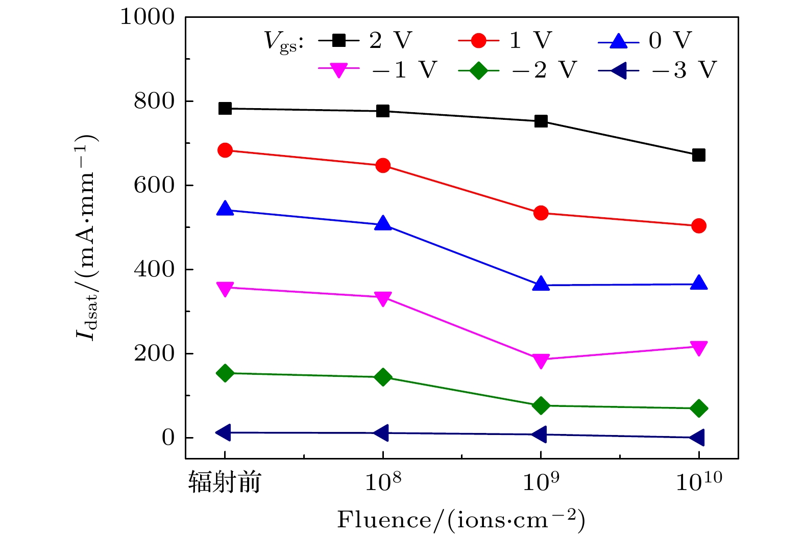
图 3 重离子辐射前后不同栅压下的最大饱和电流
Fig. 3. Maximum saturation current under different gate voltages before and after heavy ion radiation.

图 4 重离子辐射前后EMMI测试结果图 (a)辐射前; (b) 1×10⁸ ions/cm2; (c) 1×10⁹ ions/cm2; (d) 1×10¹⁰ ions/cm2
Fig. 4. EMMI test results before and after heavy ion radiation: (a) Before radiation; (b) 1×10⁸ ions/cm2; (c) 1×10⁹ ions/cm2; (d) 1×10¹⁰ ions/cm2.

图 5 辐射前器件在不同栅压下的噪声测试结果
Fig. 5. Noise test results of the devices under different gate voltages before irradiation.

图 6 重离子辐射前后漏极电流噪声归一化功率谱密度与频率的关系
Fig. 6. Relationship between frequency and normalized power spectral density of drain current noise before and after heavy ion radiation.

图 7 重离子辐射前后归一化漏极电流噪声与漏极电流的函数关系
Fig. 7. Normalized drain current noise as a function of drain current before and after heavy ion irradiation.

图 8 辐射前后Hooge参数和过驱动电压的关系
Fig. 8. Relationship between Hooge parameters and overdrive voltage before and after heavy ion irradiation.
-
[1] Baliga B J 2013 Semicond. Sci. Technol. 28 074011
Google Scholar
[2] Amano H, Baines Y, Beam E, et al. 2018 J. Phys. D Appl. Phys. 51 163001
Google Scholar
[3] Nedelcescu A I, Carlone C, Houdayer A, Bardeleben H J, Cantin J L, Raymond S 2002 IEEE Trans. Nucl. Sci. 49 2733
Google Scholar
[4] Pearton S J, Hwang Y S, Ren F 2015 JOM 67 1601
Google Scholar
[5] 吕玲, 张进城, 李亮, 马晓华, 曹艳荣, 郝跃 2012 物理学报 61 057202
Google Scholar
Lü L, Zhang J C, Li L, Ma X H, Cao Y R, Hao Y 2012 Acta Phys. Sin. 61 057202
Google Scholar
[6] 郝蕊静, 郭红霞, 潘霄宇, 吕玲, 雷志锋, 李波, 钟向丽, 欧阳晓平, 董世剑 2020 物理学报 69 207301
Google Scholar
Hao R J, Guo H X, Pan X Y, Lü L, Lei Z F, Li B, Zhong X L, Ouyang X P Dong S J 2020 Acta Phys. Sin. 69 207301
Google Scholar
[7] Jiang R, Zhang E X, McCurdy M W, Chen J, Shen X, Wang P, Fleetwood D M, Schrimpf R D, Kaun S W, Kyle E C H, Speck J S, Pantelides S T 2017 IEEE Trans. Nucl. Sci. 64 218
Google Scholar
[8] Pearton S J, Ren F, Patrick E, Law M E, Polyakov A Y 2016 ESC J. Solid State Sc. 5 Q35
Google Scholar
[9] Bazzoli S, Girard S, Ferlet-Cavrois V, Baggio J, Duhamel O 2007 9th European Conference on Radiation and its Effects on Components and Systems Deauville France, Septemper 10–14, 2007 p1
[10] Kuboyama S, Maru A, Shindou H, Ikeda N, Hirao T, Abo H, Tamura T 2011 IEEE Trans. Nucl. Sci. 58 2734
Google Scholar
[11] Martinez M J, King M P, Baca A G, Allerman A A, Armstrong A A, Klein B A, Douglas E A, Kaplar R J, Swanson S E 2019 IEEE Trans. Nucl. Sci. 66 344
Google Scholar
[12] Rostewits M, Hirche K, Latti J, Jutzi E 2013 IEEE Trans. Nucl. Sci. 60 2525
Google Scholar
[13] Sonia G, Brunner F, Denker A, Lossy R, Mai M, Opitz-Coutureau J, Pensl G, Richter E, Schmidt J, Zeimer U, Wang L, Weyers M, Wurfl J, Trankle G 2006 IEEE Trans. Nucl. Sci. 53 3661
Google Scholar
[14] Lei Z, Guo H, Tang M, Chang Z, Hui C, Zhang Z 2016 16th European Conference on Radiation and its Effects on Components and Systems Bremen Germany, Septemper 19–23, 2016 p1
[15] Sasaki H, Hisaka T, Kadoiwa K, Oku T, Onode S, Ohshima T, Taguchi E, Yasude H 2017 Microelectron. Reliab. 81 312
Google Scholar
[16] Hu P P, Liu J, Zheng S X, Maaz K, Zeng J, Zhai P F, Xu L J, Cao Y R, Duan J L, Li Z Z, Sun Y M, Ma X H 2018 Nucl. Instrum. Meth. B 430 59
Google Scholar
[17] Challa S R, Vega N A, Mueller N A, Kristukat C, Debray M E, Witte H, Dadgar A, Strittmatter A 2021 IEEE T. ELectron Dev. 68 24
Google Scholar
[18] 魏峰 2007 硕士学位论文 (上海: 复旦大学)
Wei F 2007 M. S. Thesis (Shanghai: Fudan University
[19] Tartarin J G 2011 21th International Conference on Noise and Fluctyations Toronto, Canada, June 12−16, 2011 p452
[20] 刘宇安, 庄奕琪, 杜磊, 苏亚慧 2013 物理学报 62 140703
Google Scholar
Liu Y A, Zhuang T Q, Du L, Su Y H 2013 Acta Phys. Sin. 62 140703
Google Scholar
[21] Cai Y, Zhou Y, Lau K M, Chen K J 2006 IEEE T. Electron Dev. 53 2207
Google Scholar
[22] Sitvestri M, Uren M J, Killat N, Marcon D, Kuball M 2013 Appl. Phys. Lett. 103 043506
Google Scholar
[23] Ghibaudo G, Roux O, Nguyen-Duc C, Balestra F, Brini J 1991 Phys. Status Solidi 124 571
Google Scholar
[24] Watkins T B 1959 Proceed. Phys. Soc. 73 59
Google Scholar
[25] Vodapally S, Jang Y I, Kang I M, Cho I T, Lee J H, Bae Y, Ghibaudo G, Cristoloveanu S, Im K S, Lee G H 2017 IEEE Electr. Dev. Lett. 38 252
Google Scholar
[26] Chen Y Q, Zhang Y C, Liu Y, Liao X Y, Huang Y 2018 IEEE Trans. Electron Dev. 65 1321
Google Scholar
[27] Hooge F N 1994 IEEE Trans. Electron. Dev. 41 1926
Google Scholar
[28] Achouche M, Biblemont S 1996 Electron. Lett. 32 1326
Google Scholar


 下载:
下载:

计量
- 文章访问数: 887
- PDF下载量: 36
- 被引次数: 0
