


-
在显示领域, 微型发光二极管 (micro-LED) 潜力巨大, 有望引领下一代新型显示技术的发展方向, 其显示性能在很多方面优于现有的液晶、有机发光二极管(OLED), 但巨量的micro-LED像素点与驱动电路不在同一晶圆上制备, 面临巨量转移的技术瓶颈. 本文将新兴的石墨烯场效应晶体管作为驱动元件与氮化镓 (GaN) micro-LED进行单片集成, 因为二者直接制备于同一衬底上, 所以从根源上规避了巨量转移的技术难题. 此外, 传统光刻工艺中紫外光刻胶直接接触石墨烯, 会引入严重掺杂导致场效应晶体管性能较差, 进而影响集成器件性能. 本文提出了一种利用聚甲基丙烯酸甲酯(PMMA)薄膜作为保护层, 直接旋涂紫外光刻胶进行垫层光刻的全新工艺方法, 优化了石墨烯场效应晶体管制备工艺. 首先在分立的石墨烯场效应晶体管中进行验证, 相比于没有进行PMMA薄膜保护的器件, 采用新工艺制备的石墨烯器件狄拉克点的栅极电压 (Vg) 距零点的偏差降低了22 V, 载流子迁移率提升了32%. 此外, 将新工艺应用到集成器件制备后, 发现集成器件性能得到了大幅提升. 利用此新技术, 由于有PMMA的保护, 紫外光刻胶不再与敏感的石墨烯沟道直接接触. 掺杂效应和随之而来的器件性能下降被有效扼制. 因为此技术简便而廉价, 所以也可应用到石墨烯之外的其他二维材料中, 例如MoS2和h-BN, 有望对本领域的器件工程师产生一定的参考价值.In the information display field, micro-light-emitting diodes (micro-LEDs) possess high potentials and they are expected to lead the direction of developing the next-generation new display technologies. Their display performances are superior to those produced by the currently prevailing liquid crystal and organic light-emitting diode based technologies. However, the micro-LED pixels and their driving circuits are often fabricated on different wafers, which implies that the so-called mass transfer seems to be inevitable, thus facing an obvious bottleneck. In this paper, the emerging graphene field effect transistors are used as the driving elements and integrated onto the GaN micro-LEDs, which is because the pixels and drivers are prepared directly on the same wafer, the technical problem of mass transfer is fundamentally bypassed. Furthermore, in traditional lithographic process, the ultraviolet photoresist directly contacts the graphene, which introduces severe carrier doping, thereby leading to deteriorated graphene transistor properties. This, not surprisingly, further translates into lower performances of the integrated devices. In the present work, proposed is a technique in which the polymethyl methacrylate (PMMA) thin films act as both the protection layers and the interlayers when optimizing the graphene field effect transistor processing. The PMMA layers are sandwiched between the graphene and the ultraviolet photoresist, which is a brand new device fabrication process. First, the new process is tested in discrete graphene field effect transistors. Compared with those devices that are processed without the PMMA protection thin films, the graphene devices fabricated with the new technology typically show their Dirac point at a gate voltage (Vg) deviation from Vg = 0, that is, 22 V lower than their counterparts. In addition, an increase in the carrier mobility of 32% is also observed. Finally, after applying the newly developed fabrication process to the pixel-and-driver integrated devices, it is found that their performances are improved significantly. With this new technique, the ultraviolet photoresist no longer directly contacts the sensitive graphene channel because of the PMMA protection. The doping effect and the performance dropping are dramatically reduced. The technique is facile and cheap, and it is also applicable to two-dimensional materials besides graphene, such as MoS2 and h-BN. It is hoped that it is of some value for device engineers working in this field.
-
Keywords:
- graphene /
- gallium nitride /
- micro-light emitting diode /
- polymethyl methacrylate
[1] Wu T Z, Sher C W, Lin Y, Lee C F, Liang S J, Lu Y J, Chen S W H, Guo W J, Kuo H C, Chen Z 2018 Appl. Sci. -Basel. 8 1557
 Google Scholar
[2] Ding K, Avrutin V, Lzyumskaya N, Ozgur U, Morkoc H 2019 Appl. Sci. -Basel. 9 1206
Google Scholar
[3] Liu Z J, Huang T D, Ma J, Liu C, Lau K M 2014 IEEE Electron Device Lett. 35 330
Google Scholar
[4] Lee Y J, Yang Z P, Chen P G, Hsieh Y A, Yao Y C, Liao M H, Lee M H, Wang M T, Hwang J M 2014 Opt. Express 22 A1589
Google Scholar
[5] Fu Y, Sun J, Du Z, Guo W, Yan C, Xiong F, Wang L, Dong Y, Xu C, Deng J Gun T, Yan Q 2019 Materials 12 428
Google Scholar
[6] Novoselov K S, Geim A K, Morozov S V, Jiang D, Zhang Y, Dubonos S V, Grigorieva, Firsov A A 2004 Science 306 666
Google Scholar
[7] Bolotin K I, Sikes K J, Jiang Z, Klima M, Fudenberg G, Hone J, Kim P, Stormer H L 2008 Solid State Commun. 146 351
Google Scholar
[8] Sul O, Kim K, Choi E, Kil J, Park W, Lee S B 2016 Nanotechnol. 27 505205
Google Scholar
[9] Lin Y C, Lu C C, Yeh C H, Jin C H, Suenaga K, Chiu P W 2012 Nano Lett. 12 414
Google Scholar
[10] Shao P Z, Zhao H M, Cao H W, Wang X F, Pang Y, Li Y X, Deng N Q, Zhang J, Zhang G Y, Yang Y, Zhang S, Ren T L 2016 Appl. Phys. Lett. 108 203105
Google Scholar
[11] Zhang H, Guo X, Niu W, Bao W Z 2020 2D Mater 7 025019
Google Scholar
[12] Reina A, Jia X T, Ho J, Nezich D, Son H, Bulovic V, Dresselhaus MS, Kong J 2009 Nano Lett. 9 30
Google Scholar
[13] Li X S, Cai W W, An J H, Kim S, Nah J, Yang D, Piner R, Velamakanni A, Jung I, Tutuc E, Banerjee S K, Colombo L, Ruoff R 2009 Science 324 1312
Google Scholar
[14] Kang J, Liu W, Banerjee K 2014 Appl. Phys. Lett. 104 093106
Google Scholar
[15] Wu D, Zhang Z, Lv D, Peng Z 2016 Mater. Express 6 198
Google Scholar
[16] Radisavljevic B, Radenovic A, Brivio J, Giacometti V, Kis A 2011 Nat. Nanotechnol. 6 147
Google Scholar
[17] Dean C R, Young A F, Meric I, Lee C, Wang L, Sorgenfrei K, Taniguchi T, Kim P, Shepard K L, Hone J 2010 Nat. Nanotechnol. 5 722
Google Scholar
[18] Li L, Yu Y, Ye G, Ge Q, Ou X, Wu H, Feng D, Chen X, Zhang Y 2014 Nat. Nanotechnol. 9 372
Google Scholar
[19] Ni Z, Wang Y, Yu T, Shen Z 2008 Nano Res. 1 273
Google Scholar
[20] Lara-Avila S, Moth-Poulsen K, Yakimova R, Bjrnholm T, Falko V, Tzalenchuk A, Kubatkin S 2011 Adv. Mater. 23 878
Google Scholar
[21] Chen J H, Jang C, Xiao S, Ishigami M, Fuhrer M S 2008 Nat. Nanotechnol. 3 206
Google Scholar
-
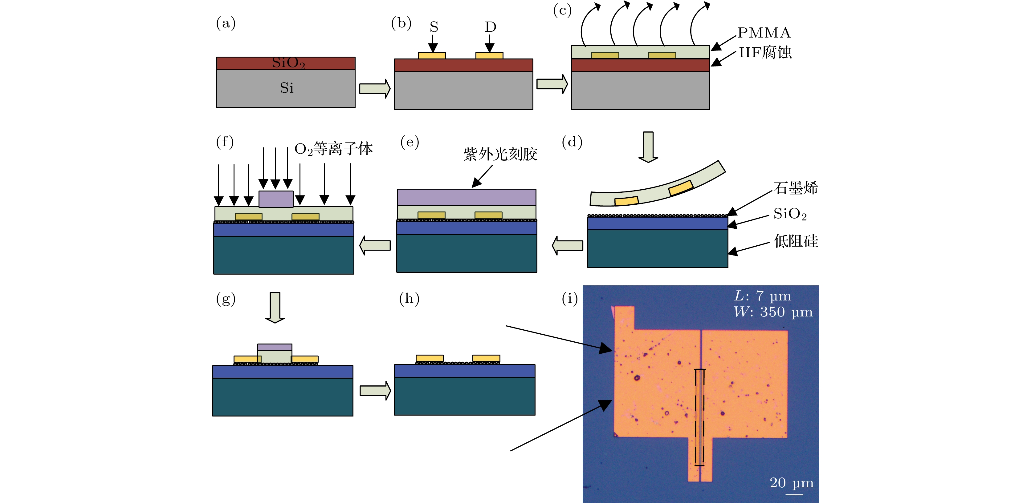
图 1 基于PMMA作为载体转移图形化电极并进行石墨烯垫层光刻的新工艺的石墨烯晶体管制备流程图
Fig. 1. Fabricated process of graphene transistor based on PMMA as the carrier to transfer patterned electrode and followed by graphene photolithography with PMMA underlayer.
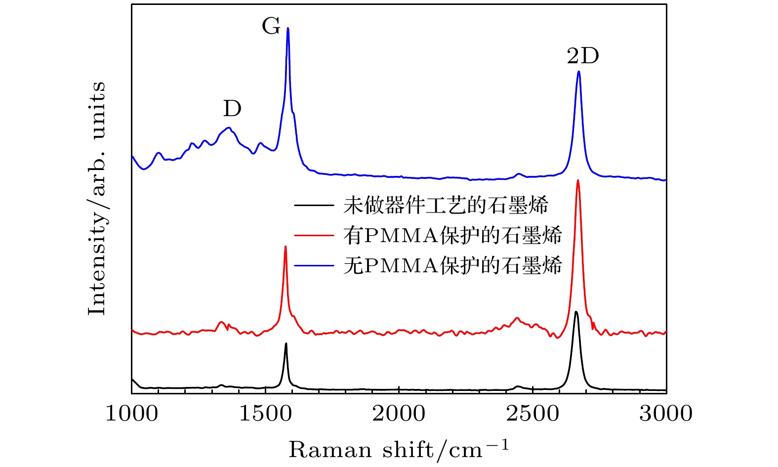
图 2 未做器件工艺的石墨烯(黑色曲线)、有PMMA保护的石墨烯沟道(红色曲线)、无PMMA保护的石墨烯沟道的拉曼光谱(蓝色曲线)
Fig. 2. Raman spectra of the graphene that does not undergo any device processing (black curve), graphene channel with PMMA protection (red curve), and graphene channel without PMMA protection (blue curve).
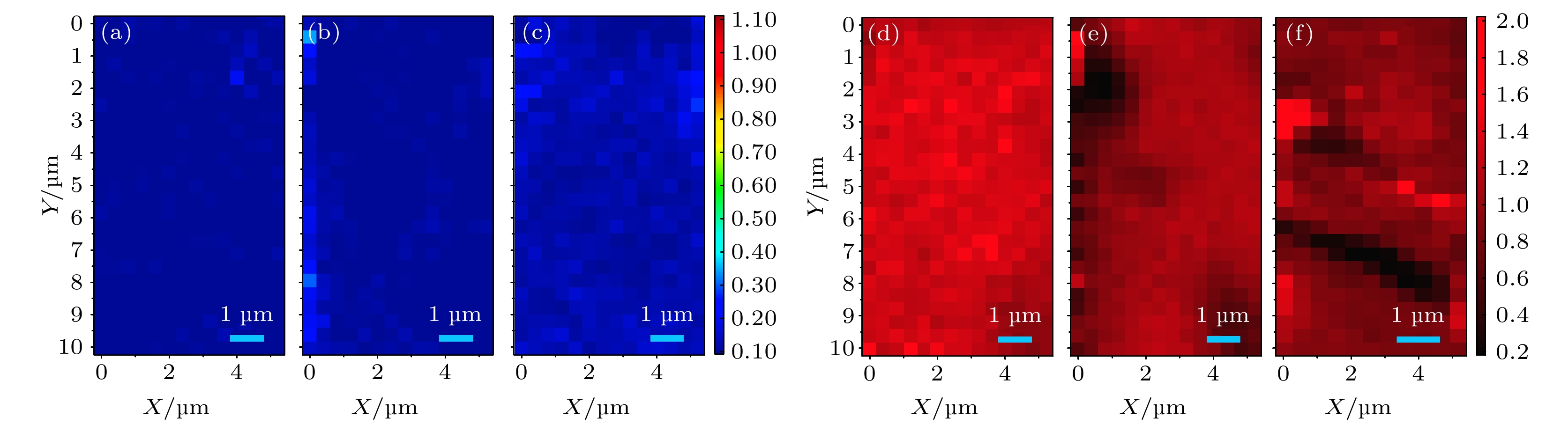
图 3 (a), (b), (c)分别是未做工艺的石墨烯、新工艺有PMMA保护、旧工艺无PMMA保护ID/IG拉曼显微成像; (d), (e), (f)分别是未做工艺的石墨烯、新工艺有PMMA保护、旧工艺无PMMA保护I2 D/IG拉曼显微成像
Fig. 3. (a), (b), (c) are ID/IG Raman mapping of graphene without processing, graphene with new processing with PMMA protection, and graphene with old processing with no PMMA protection, respectively; (d), (e), (f) are I2 D/IG Raman mapping of graphene without processing, graphene with new processing with PMMA protection, and graphene with old processing with no PMMA protection, respectively.
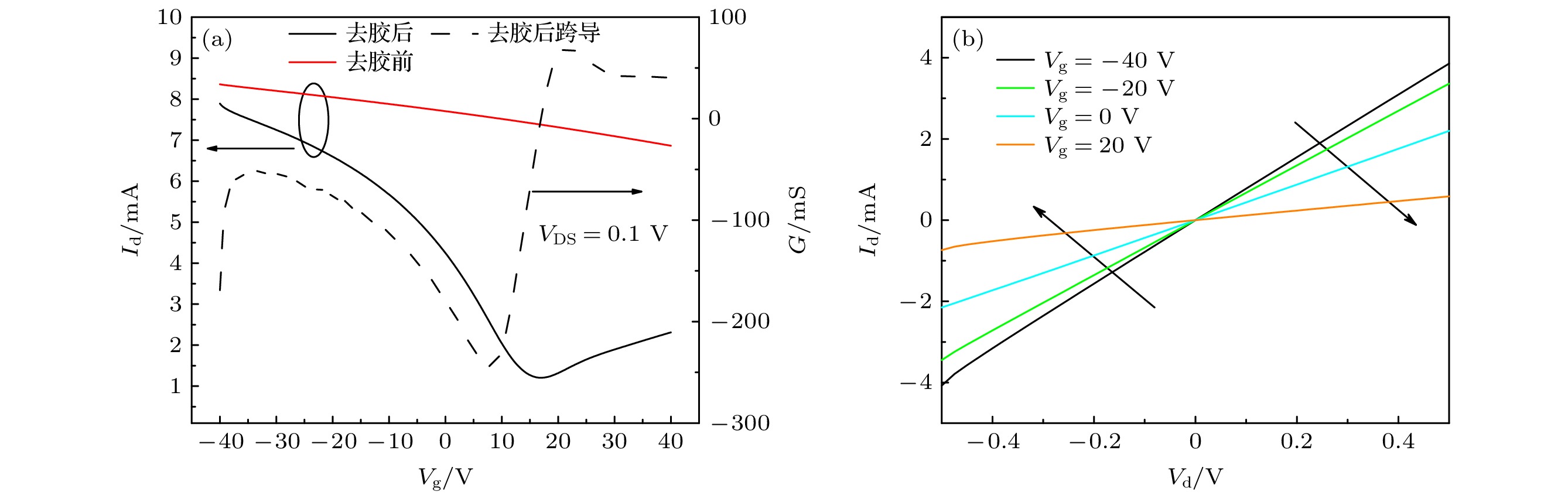
图 4 (a)在有PMMA垫层保护的情况下, 去胶前后石墨烯场效应晶体管的转移特性曲线; (b) 优化后石墨烯场效应晶体管在室温下的输出特性曲线
Fig. 4. (a) In the case of PMMA underlayer protection, the transfer characteristic curve before and after removing the resist from the graphene field effect transistor; (b) output characteristic curves of the optimized graphene field effect transistor at room temperature.
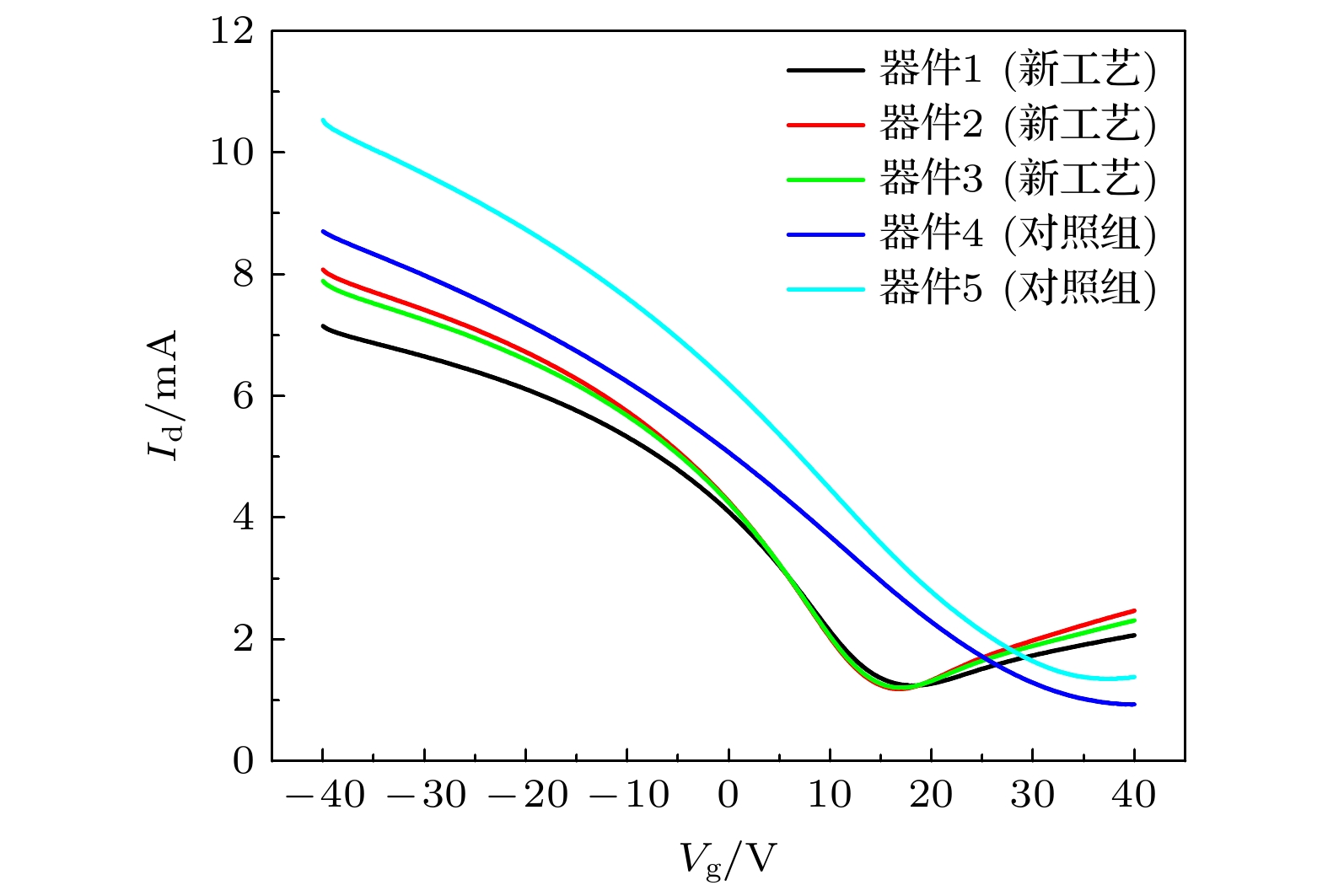
图 5 有无PMMA保护工艺过程的石墨烯场效应晶体管转移特性曲线
Fig. 5. Transfer characteristic curves of graphene field effect transistors with and without PMMA protection processing.
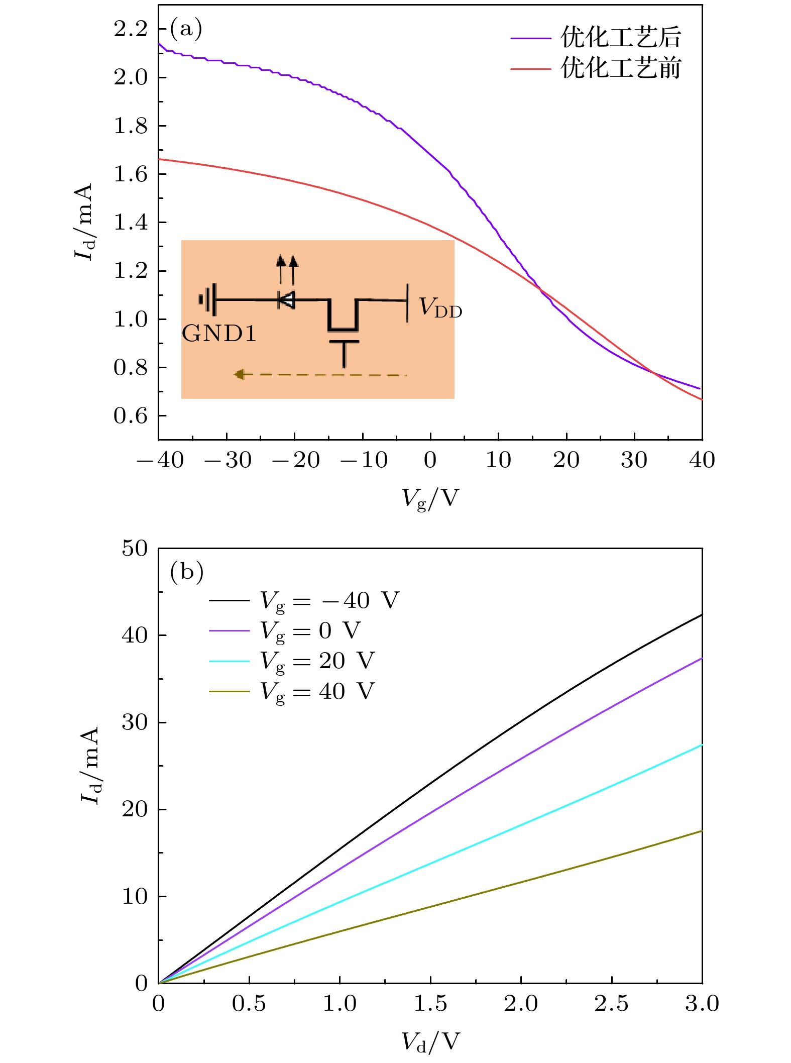
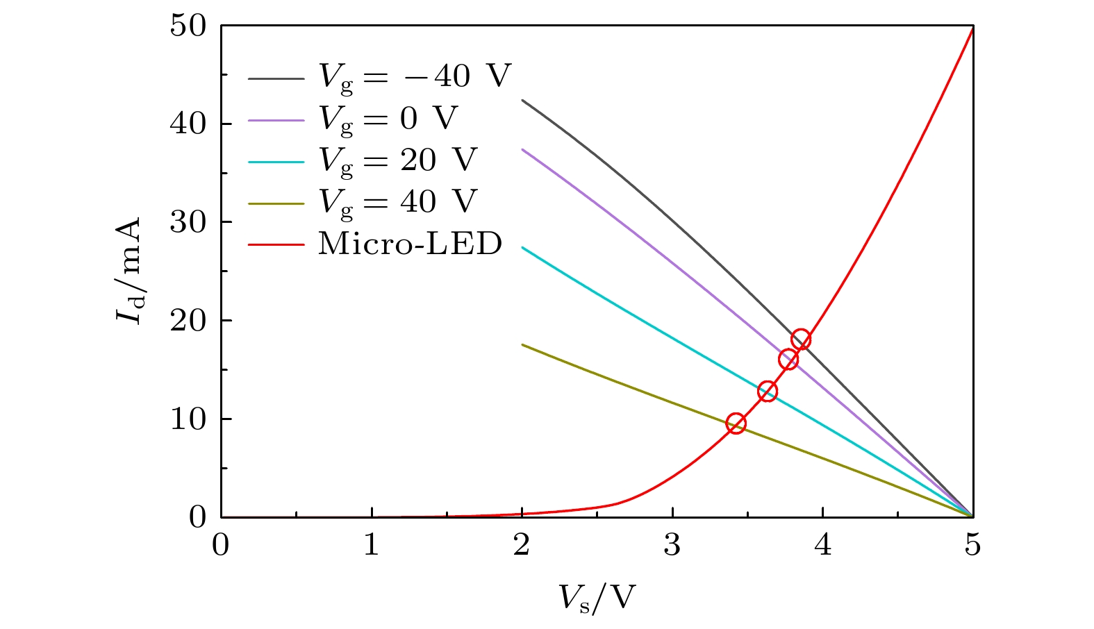
图 6 室温下石墨烯场晶体管的场效应特性曲线 (a)转移曲线(插图为集成器件等效电路图); (b)输出曲线
Fig. 6. Field effect characteristic curve of graphene transistor at room temperature: (a) Transfer curve (The insert show the equivalent circuit diagram of the integrated device); (b) output curve.
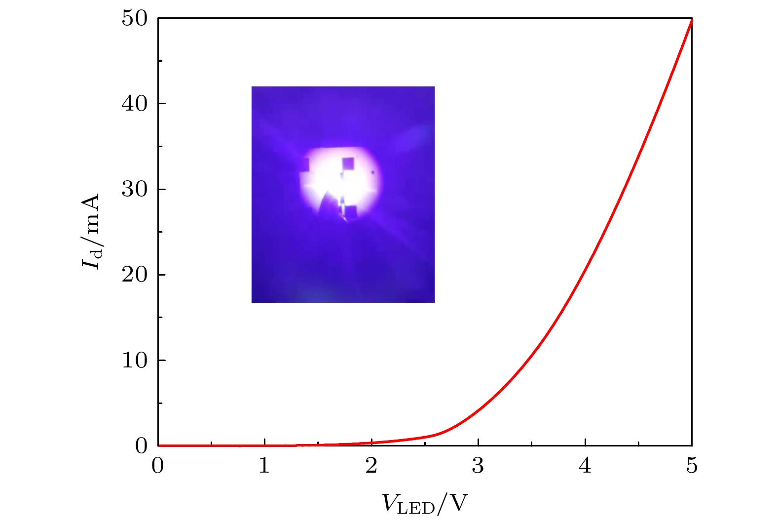
图 7 GaN micro-LED的I-V特性曲线(插图为5 V正向电压下的电致发光照片)
Fig. 7. I-V characteristic curve of the GaN micro-LED (The insert shows the light emission photo under 5 V forward voltage).
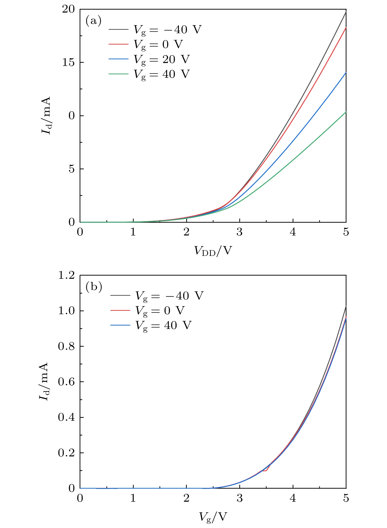
图 8 (a)采用新工艺的集成器件I-V曲线; (b)传统光刻工艺集成器件的I-V曲线
Fig. 8. I-V characteristic curves of the integrated device: (a) Based on the new process; (b) based on traditional technology.
-
[1] Wu T Z, Sher C W, Lin Y, Lee C F, Liang S J, Lu Y J, Chen S W H, Guo W J, Kuo H C, Chen Z 2018 Appl. Sci. -Basel. 8 1557
Google Scholar
[2] Ding K, Avrutin V, Lzyumskaya N, Ozgur U, Morkoc H 2019 Appl. Sci. -Basel. 9 1206
Google Scholar
[3] Liu Z J, Huang T D, Ma J, Liu C, Lau K M 2014 IEEE Electron Device Lett. 35 330
Google Scholar
[4] Lee Y J, Yang Z P, Chen P G, Hsieh Y A, Yao Y C, Liao M H, Lee M H, Wang M T, Hwang J M 2014 Opt. Express 22 A1589
Google Scholar
[5] Fu Y, Sun J, Du Z, Guo W, Yan C, Xiong F, Wang L, Dong Y, Xu C, Deng J Gun T, Yan Q 2019 Materials 12 428
Google Scholar
[6] Novoselov K S, Geim A K, Morozov S V, Jiang D, Zhang Y, Dubonos S V, Grigorieva, Firsov A A 2004 Science 306 666
Google Scholar
[7] Bolotin K I, Sikes K J, Jiang Z, Klima M, Fudenberg G, Hone J, Kim P, Stormer H L 2008 Solid State Commun. 146 351
Google Scholar
[8] Sul O, Kim K, Choi E, Kil J, Park W, Lee S B 2016 Nanotechnol. 27 505205
Google Scholar
[9] Lin Y C, Lu C C, Yeh C H, Jin C H, Suenaga K, Chiu P W 2012 Nano Lett. 12 414
Google Scholar
[10] Shao P Z, Zhao H M, Cao H W, Wang X F, Pang Y, Li Y X, Deng N Q, Zhang J, Zhang G Y, Yang Y, Zhang S, Ren T L 2016 Appl. Phys. Lett. 108 203105
Google Scholar
[11] Zhang H, Guo X, Niu W, Bao W Z 2020 2D Mater 7 025019
Google Scholar
[12] Reina A, Jia X T, Ho J, Nezich D, Son H, Bulovic V, Dresselhaus MS, Kong J 2009 Nano Lett. 9 30
Google Scholar
[13] Li X S, Cai W W, An J H, Kim S, Nah J, Yang D, Piner R, Velamakanni A, Jung I, Tutuc E, Banerjee S K, Colombo L, Ruoff R 2009 Science 324 1312
Google Scholar
[14] Kang J, Liu W, Banerjee K 2014 Appl. Phys. Lett. 104 093106
Google Scholar
[15] Wu D, Zhang Z, Lv D, Peng Z 2016 Mater. Express 6 198
Google Scholar
[16] Radisavljevic B, Radenovic A, Brivio J, Giacometti V, Kis A 2011 Nat. Nanotechnol. 6 147
Google Scholar
[17] Dean C R, Young A F, Meric I, Lee C, Wang L, Sorgenfrei K, Taniguchi T, Kim P, Shepard K L, Hone J 2010 Nat. Nanotechnol. 5 722
Google Scholar
[18] Li L, Yu Y, Ye G, Ge Q, Ou X, Wu H, Feng D, Chen X, Zhang Y 2014 Nat. Nanotechnol. 9 372
Google Scholar
[19] Ni Z, Wang Y, Yu T, Shen Z 2008 Nano Res. 1 273
Google Scholar
[20] Lara-Avila S, Moth-Poulsen K, Yakimova R, Bjrnholm T, Falko V, Tzalenchuk A, Kubatkin S 2011 Adv. Mater. 23 878
Google Scholar
[21] Chen J H, Jang C, Xiao S, Ishigami M, Fuhrer M S 2008 Nat. Nanotechnol. 3 206
Google Scholar

 下载:
下载:
计量
- 文章访问数: 3959
- PDF下载量: 97
- 被引次数: 0
