


-
Intelligent, integrated and cost-effective micro-electro-mechanical system (MEMS) and micro sensors can be developed with TiNi-based memory alloy thin film and optical fibers. Such devices can work in harsh environment, like in deep sea, in space with flammable or explosive objects, or with strong electromagnetic interference; and examples of their possible applications include gas concentration detection in underground mines, dynamic detection of production parameters in oil or gas mining, etc. As TiNi-based memory alloy thin film possesses good biocompatibility, such devices can also be used in intracranial/endocardial pressure test, surgical resection, early cancer assessment, etc. The successful development of the above MEMS and micro sensors involve optical fibers coated with memory alloy films. However, unlike the common planar substrates, optical fiber is of a cylinder with a small diameter, and how to grow good-quality memory alloy film on its surface remains to be explored. In this work, the silica fibers are coated with TiNi memory alloy films by magnetron sputtering. How to choose the proper operating parameters in the sputtering process, and also the effects of subsequent annealing treatment on the films, are discussed in detail. Uniform thin films are grown on the 125-μm-diameter cylindrical surfaces of optical fibers with our built coating mask device specially designed for fibers. The experiments show that when target-substrate distance, background vacuum degree, Ar gas flow and sputtering time are fixed in the sputtering process, the sputtering power can be optimized, while a higher sputtering pressure results in lower film deposition rate but better surface roughness. The thin film is well crystallized under annealing, and the major martensite B19′ phase and minor austenite B2 phase coexist in the Ti49.09Ni50.91 film. In the experiments, with the optimal operating parameters (sputtering power of 150 W and sputtering pressure of 0.23 Pa), TiNi memory alloy film about 852.2 nm in thickness is grown on the fiber at a deposition rate of 0.118 nm/s, and surface root mean square roughness of the unannealed film is 15.1 nm. Annealing at temperatures of 500, 550 and 600 ℃ are respectively tried, and such a thermal treatment evidently refines the crystalline grains inside the film. Surface root mean square roughness of the film annealed at 600 ℃ is reduced to 6.32 nm. This work indicates that a glass fiber can be coated with high-quality TiNi-based memory alloy film, and it thus forms a part of the bases of further development of relevant MEMS and micro sensors. -
Keywords:
- optical fiber /
- TiNi-based film /
- magnetron sputtering /
- process parameter
[1] Han S P, Meng Z, Omisore O M, Akinyemi T, Yan Y P 2020 Micromachines 11 1021
 Google Scholar
[2] 解甜, 王传礼, 喻曹丰 2019 微电机 52 72
Google Scholar
Xie T, Wang C L, Yu C F 2019 Micromotors 52 72
Google Scholar
[3] 吴建生, 吴晓东, 王征 1997 材料研究学报 5 449
Wu J S, Wu X D, Wang Z 1997 Chin. J. Mater. Res. 5 449
[4] Tan C L, Liu J, Tian X H, Zhu J C, Zhang K 2021 Results Phys. 24 104165
Google Scholar
[5] 曲炳郡, 刘晓鹏 2002 中国机械工程 13 35
Qu B J, Liu X P 2002 China Mechanical Engineering 13 35
[6] Fu Y, Du H, Huang W, Zheng S, Min H 2004 Sens. Actuators, A 112 395
Google Scholar
[7] Anna M, Vijaya T, Sudha J, Anantha P, Vladimir S 2018 Defect Diffus. Forum 4695 169
Google Scholar
[8] Gunther V, Marchenko E, Baigonakova G 2017 Mater. Today 4 4727
Google Scholar
[9] Im Y M, Noh J P, Cho G B, Nam T H 2018 Shape Mem. Superelast. 4 121
Google Scholar
[10] Nagasaki Y, Gholipour B, Ou J Y, Tsuruta M, Plum E, MacDonald K F, Takahara J, Zheludev N I 2018 Appl. Phys. Lett. 113 021105
Google Scholar
[11] Knick C R, Smith G L, Morris C J, Bruck H A 2019 Sens. Actuators, A 291 48
Google Scholar
[12] 吴佩泽, 贺志荣, 李自源, 刘康凯, 王家乐 2017 热加工工艺 46 10
Google Scholar
Wu P Z, He Z R, Li Z Y, Liu K K, Wang J L 2017 Hot Working Technology 46 10
Google Scholar
[13] 蒋建军, 胡毅, 陈星, 等 2018 材料工程 46 1
Google Scholar
Jiang J J, Hu Y, Chen X, et al. 2018 J. Mater. Engineer. 46 1
Google Scholar
[14] 刘兵飞, 刘亚冬, 张亚楠 2021 复合材料学报 38 1177
Google Scholar
Liu B F, Liu Y D, Zhang Y N 2021 Acta Mater. Compos. Sin. 38 1177
Google Scholar
[15] Zhu J N, Zeng Q F, Fu T 2019 Corros. Rev. 37 539
Google Scholar
[16] 崔俊龙, 江秀娟 2020 CN111349886A
Cui J L, Jiang X J 2020 CN111349886A (in Chinese)
[17] Kim D, Lee H, Bae J, Hyomin C, Byeongkeun N, Taehyun N 2018 J. Nanosci. Nanotechnol. 18 6201
Google Scholar
[18] 邱清泉, 励庆孚, 苏静静, Jim F 2009 真空科学与技术学报 29 46
Google Scholar
Qiu Q Q, Li Q F, Su J J, Jim F 2009 Chin. J. Vacuum Sci. Technol. 29 46
Google Scholar
[19] 窦军 2013 硕士学位论文 (长春: 吉林大学)
Dou J 2013 M. S. Thesis (Changchun: Jilin University) (in Chinese)
[20] 王利民 2008 硕士学位论文 (哈尔滨: 哈尔滨工程大学)
Wang L M 2008 M. S. Thesis (Harbin: Harbin Engineering University) (in Chinese)
[21] Otsuka K, Ren X 1999 Intermetallics 7 511
Google Scholar
[22] 刘晓鹏 2002 博士学位论文 (大连: 大连理工大学)
Liu X P 2002 Ph. D. Dissertation (Dalian: Dalian University of Technology) (in Chinese)
[23] Fu Y Q, Du H J, Zhang S, Gu Y W 2005 Surf. Coat. Tech. 198 389
Google Scholar
[24] 李艳锋, 米绪军, 尹向前, 高宝东 2011 材料热处理学报 32 11
Google Scholar
Li Y F, Mi X J, Yi X Q, Gao B D 2011 T. Mater. Heat Treat. 32 11
Google Scholar
[25] 于孟, 薛飒, 贾兵然, 毛江虹, 牛中杰 2016 稀有金属 40 877
Google Scholar
Yu M, Xue S, Jia B R, Mao J H, Niu Z J 2016 Chin. J. Rare Metals 40 877
Google Scholar
[26] Zhang L, Xie C, Wu J 2007 Mater. Charact. 58 471
Google Scholar
[27] 踪敬珍 2017 硕士学位论文 (上海: 上海交通大学)
Zong J Z 2017 M. S. Thesis (Shanghai: Shanghai Jiao Tong University) (in Chinese)
[28] 林福柱 2012 硕士学位论文 (长春: 吉林大学)
Lin F Z 2012 M. S. Thesis (Changchun: Jilin University) (in Chinese)
[29] Zhang L, Xie C J, Wu J S 2007 J. Alloys Compd. 427 238
Google Scholar
[30] Sanjabi S, Sadrnezhaad S K, Yates K A, Barber Z H 2005 Thin Solid Films 419 190
Google Scholar
[31] 徐娇, 寇生中, 赵燕春, 袁小鹏, 李春燕 2014 稀有金属 38 641
Google Scholar
Xu J, Kou S Z, Zhao Y C, Yuan X P, Li C Y 2014 Chin. J. Rare Metals 38 641
Google Scholar
[32] Otsuka K, Ren X 2005 Prog. Mater. Sci. 50 511
Google Scholar
[33] Entemeyer D, Patoor E, Eberhardt A, Berveiller M 2000 Int. J. Plasticity 16 1269
Google Scholar
[34] Kumar A, Kannan M D, Jayakumar S, Rajam K S, Raju V S 2006 Surf. Coat. Tech. 201 3253
Google Scholar
-
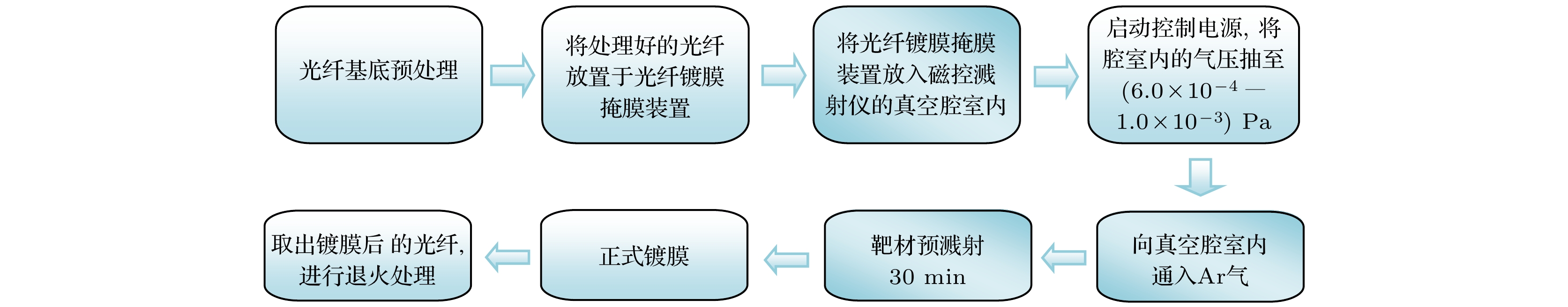
图 1 薄膜制备工艺流程
Figure 1. Preparation process of the thin film.

图 2 光纤基底的清洗工艺
Figure 2. Cleaning process of optical fiber substrate.
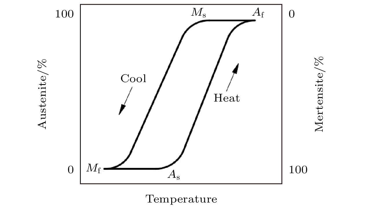
图 3 记忆合金薄膜相变示意图
Figure 3. Schematic diagram of phase transition of memory alloy thin film.
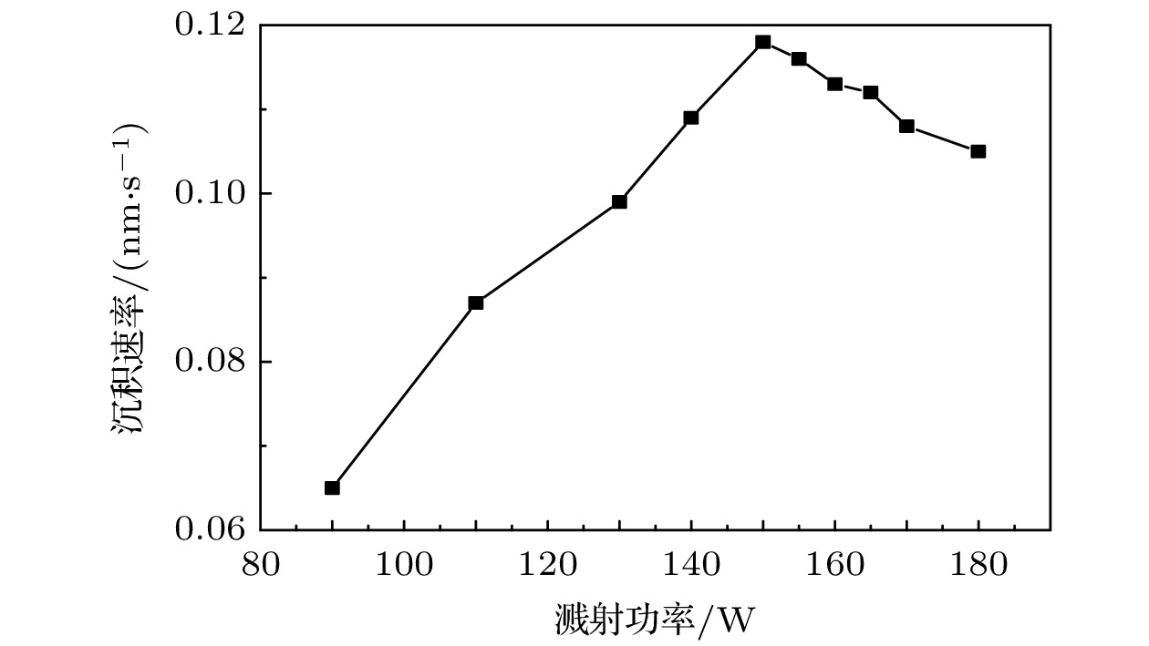
图 4 TiNi薄膜沉积速率与溅射功率的关系曲线
Figure 4. Deposition rate of TiNi thin film against sputtering power.
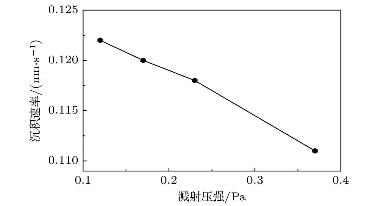
图 5 溅射压强与薄膜沉积速率的关系曲线
Figure 5. Deposition rate of TiNi thin film against sputtering pressure.
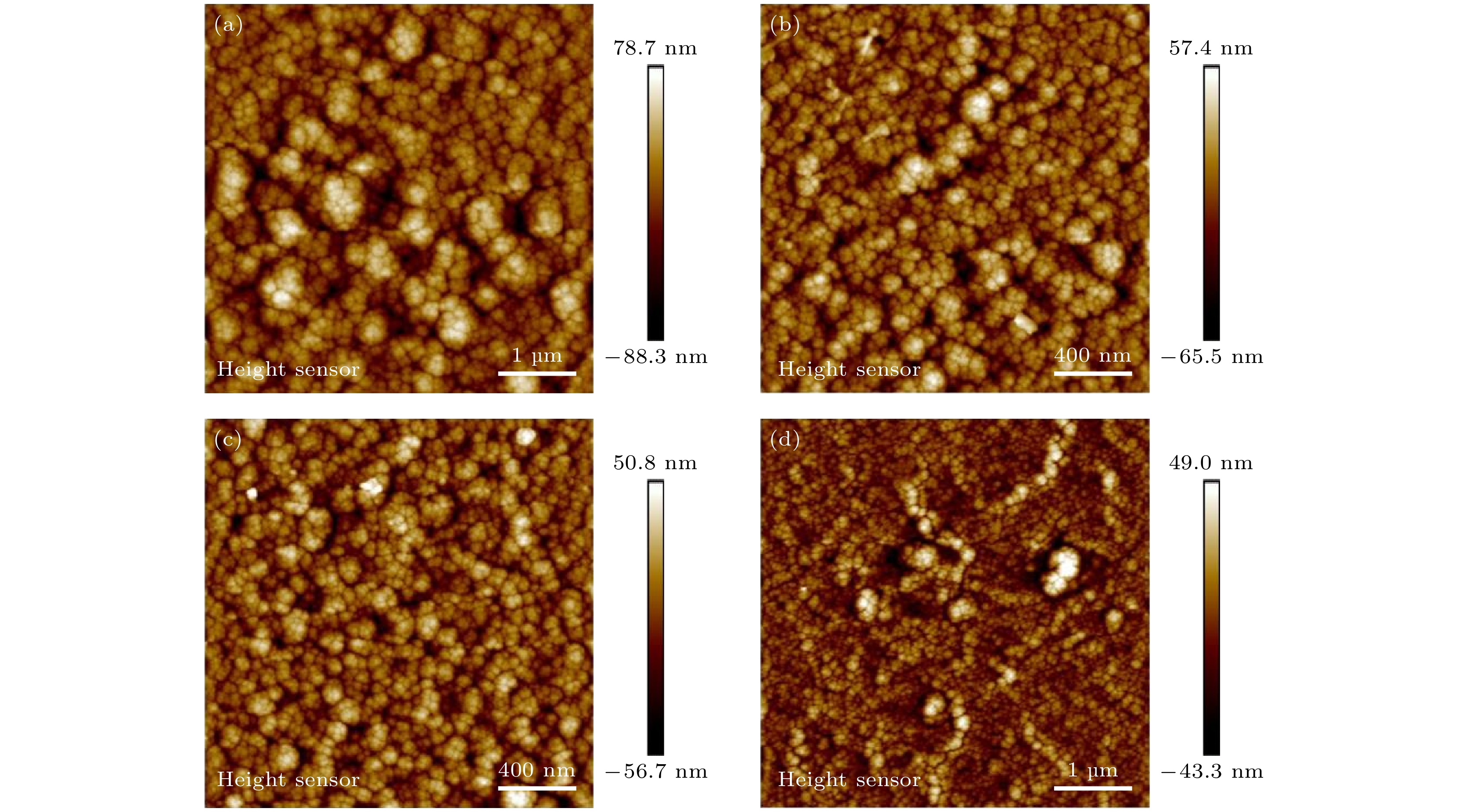
图 6 不同溅射压强下的TiNi薄膜表面二维形貌(溅射功率为150 W) (a) 0.12 Pa; (b) 0.17 Pa; (c) 0.23 Pa; (d) 0.37 Pa
Figure 6. Two-dimensional surface topography of TiNi thin films under different sputtering pressures (the sputtering power is 150 W): (a) 0.12 Pa; (b) 0.17 Pa; (c) 0.23 Pa; (d) 0.37 Pa.

图 7 不同溅射压强下的TiNi薄膜表面三维形貌图(溅射功率为150 W) (a) 0.12 Pa; (b) 0.17 Pa; (c) 0.23 Pa; (d) 0.37 Pa
Figure 7. Three-dimensional surface topography of TiNi thin films under different sputtering pressures (the sputtering power is 150 W): (a) 0.12 Pa; (b) 0.17 Pa; (c) 0.23 Pa; (d) 0.37 Pa.
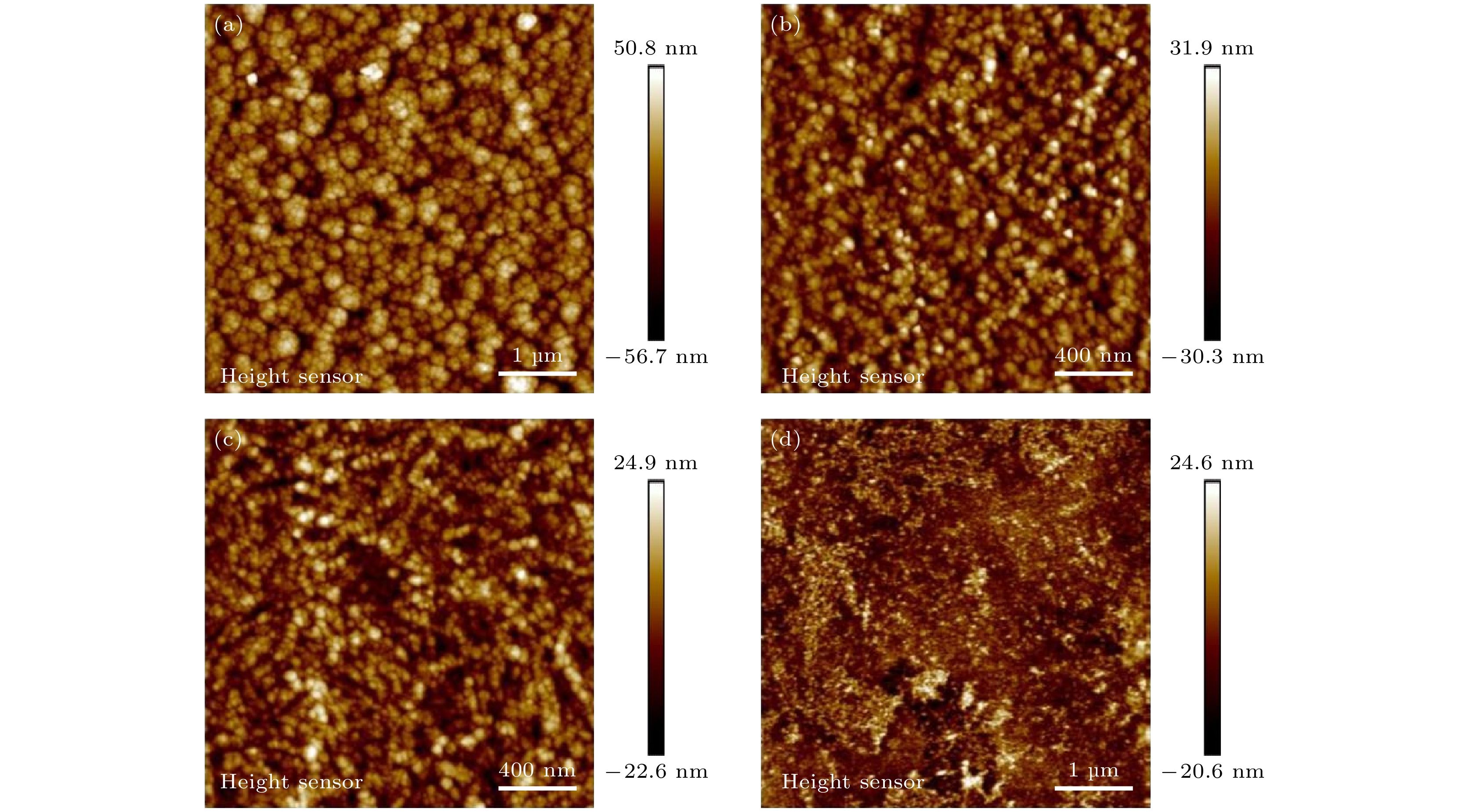
图 8 不同退火温度下TiNi薄膜表面二维形貌图(薄膜的溅射功率为150 W, 溅射压强为0.23 Pa) (a)未退火; (b) 500 ℃; (c) 550 °C; (d) 600 ℃
Figure 8. Surface morphology of TiNi thin films annealed at different temperatures: (a) Unannealed; (b) 500 ℃; (c) 550 ℃; (d) 600 ℃. The films are fabricated under the sputtering power of 150 W and the sputtering pressure of 0.23 Pa.

图 9 不同退火温度下TiNi薄膜表面三维形貌图 (a)未退火; (b) 500 ℃; (c) 550 ℃; (d) 600 ℃
Figure 9. Three-dimensional surface topography of TiNi thin films annealed at different temperatures: (a) Unannealed; (b) 500 ℃; (c) 550 ℃; (d) 600 ℃.
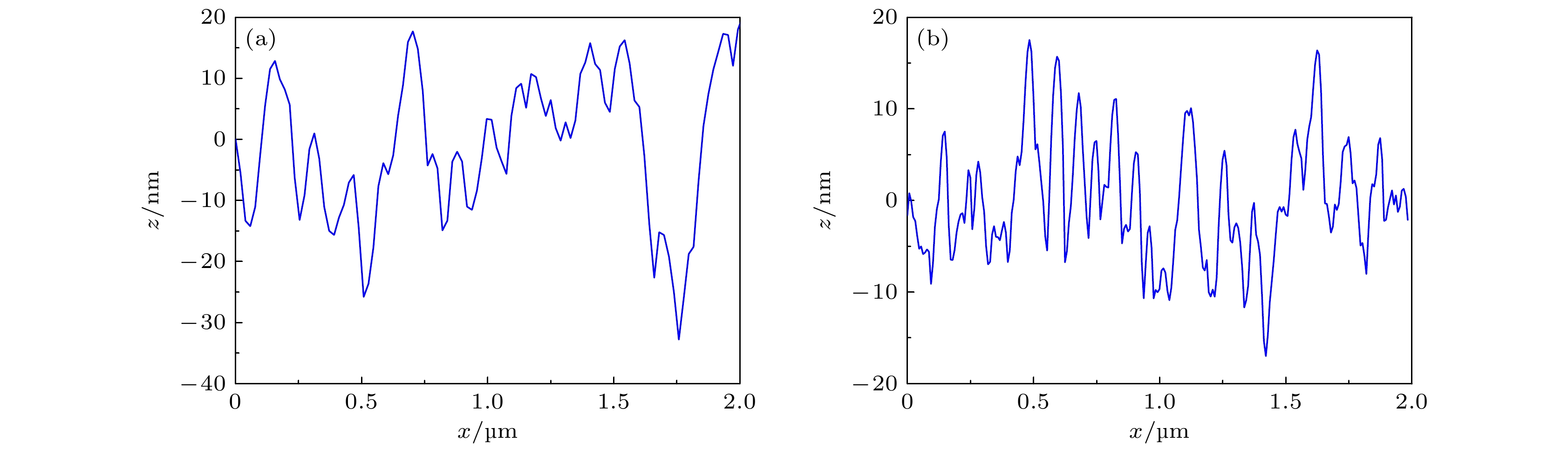
图 10 TiNi薄膜剖面图 (a)退火前; (b) 550 ℃退火后
Figure 10. Surface profile of TiNi thin films: (a) Unannealed; (b) annealed at 550 ℃.
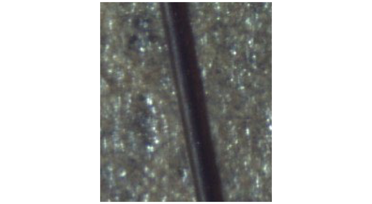
图 11 二氧化硅光纤上制备成的TiNi薄膜, 光纤包层直径为125 μm
Figure 11. TiNi film on the silica fiber, where the cladding diameter of the fiber is 125 μm.
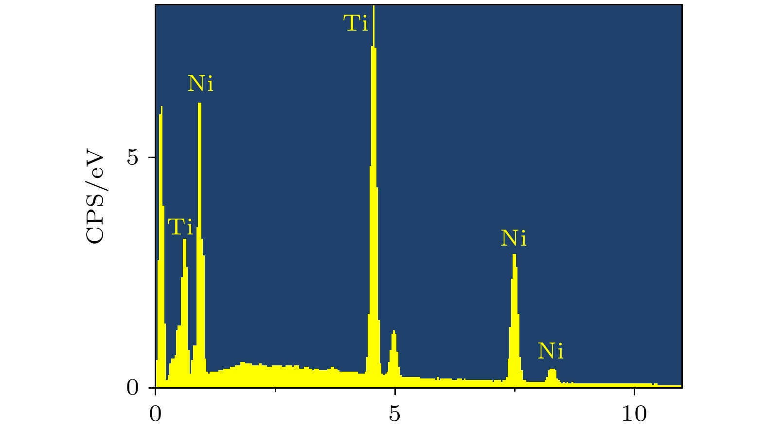
图 12 TiNi薄膜能谱图
Figure 12. Energy spectrum of TiNi thin film.
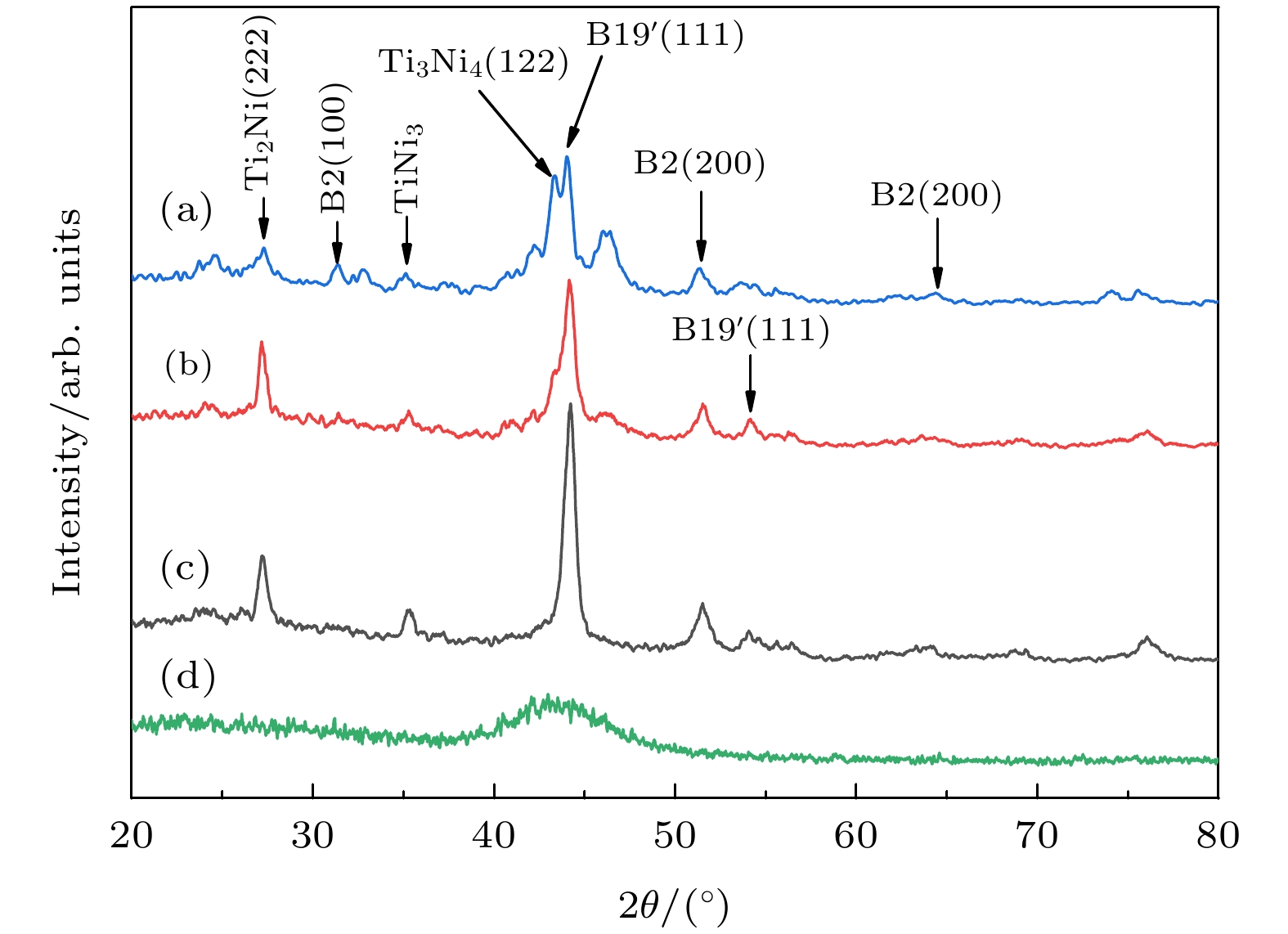
图 13 溅射态与经过不同温度退火处理的Ti49.09Ni50.91薄膜的XRD图谱比较, (a), (b)和(c)的退火温度分别为500, 550, 600 ℃, (d) 为溅射态
Figure 13. Comparison of XRD diffraction patterns of the sputtered Ti49.09Ni50.91 film and of those annealed at different temperatures: (a) Annealed at 500 ℃; (b) annealed at 550 ℃; (c) annealed at 600 ℃; (d) in sputtered state.
表 1 不同溅射功率下的薄膜厚度及沉积速率
Table 1. TiNi film thickness and deposition rate under different sputtering power.
溅射功率/W 90 110 130 140 150 155 160 165 170 180 薄膜厚度/nm 466.7 623.0 711.5 785.4 852.2 832.3 811.5 805.9 776.3 755.8 沉积速率/(nm·s–1) 0.065 0.087 0.099 0.109 0.118 0.116 0.113 0.112 0.108 0.105  DownLoad: CSV
表 2 不同溅射压强下的薄膜厚度及沉积速率
Table 2. TiNi film thickness and deposition rate under different sputtering pressure.
溅射压强/Pa 0.12 0.17 0.23 0.37 薄膜厚度/nm 875.6 864.0 852.2 795.6 沉积速率/(nm·s–1) 0.122 0.120 0.118 0.111
DownLoad: CSV
表 3 不同溅射压强下薄膜表面的均方根粗糙度
Table 3. Root mean square roughness of film surface under different sputtering pressure
溅射压强/Pa 0.12 0.17 0.23 0.37 Rq/nm 22.8 16.8 15.1 11.2
DownLoad: CSV
表 4 不同退火温度下薄膜表面的均方根粗糙度
Table 4. Surface root mean square roughness of thin films annealed at different temperatures.
退火温度/℃ 室温 500 550 600 Rq/nm 15.1 9.74 7.23 6.32
DownLoad: CSV
-
[1] Han S P, Meng Z, Omisore O M, Akinyemi T, Yan Y P 2020 Micromachines 11 1021
Google Scholar
[2] 解甜, 王传礼, 喻曹丰 2019 微电机 52 72
Google Scholar
Xie T, Wang C L, Yu C F 2019 Micromotors 52 72
Google Scholar
[3] 吴建生, 吴晓东, 王征 1997 材料研究学报 5 449
Wu J S, Wu X D, Wang Z 1997 Chin. J. Mater. Res. 5 449
[4] Tan C L, Liu J, Tian X H, Zhu J C, Zhang K 2021 Results Phys. 24 104165
Google Scholar
[5] 曲炳郡, 刘晓鹏 2002 中国机械工程 13 35
Qu B J, Liu X P 2002 China Mechanical Engineering 13 35
[6] Fu Y, Du H, Huang W, Zheng S, Min H 2004 Sens. Actuators, A 112 395
Google Scholar
[7] Anna M, Vijaya T, Sudha J, Anantha P, Vladimir S 2018 Defect Diffus. Forum 4695 169
Google Scholar
[8] Gunther V, Marchenko E, Baigonakova G 2017 Mater. Today 4 4727
Google Scholar
[9] Im Y M, Noh J P, Cho G B, Nam T H 2018 Shape Mem. Superelast. 4 121
Google Scholar
[10] Nagasaki Y, Gholipour B, Ou J Y, Tsuruta M, Plum E, MacDonald K F, Takahara J, Zheludev N I 2018 Appl. Phys. Lett. 113 021105
Google Scholar
[11] Knick C R, Smith G L, Morris C J, Bruck H A 2019 Sens. Actuators, A 291 48
Google Scholar
[12] 吴佩泽, 贺志荣, 李自源, 刘康凯, 王家乐 2017 热加工工艺 46 10
Google Scholar
Wu P Z, He Z R, Li Z Y, Liu K K, Wang J L 2017 Hot Working Technology 46 10
Google Scholar
[13] 蒋建军, 胡毅, 陈星, 等 2018 材料工程 46 1
Google Scholar
Jiang J J, Hu Y, Chen X, et al. 2018 J. Mater. Engineer. 46 1
Google Scholar
[14] 刘兵飞, 刘亚冬, 张亚楠 2021 复合材料学报 38 1177
Google Scholar
Liu B F, Liu Y D, Zhang Y N 2021 Acta Mater. Compos. Sin. 38 1177
Google Scholar
[15] Zhu J N, Zeng Q F, Fu T 2019 Corros. Rev. 37 539
Google Scholar
[16] 崔俊龙, 江秀娟 2020 CN111349886A
Cui J L, Jiang X J 2020 CN111349886A (in Chinese)
[17] Kim D, Lee H, Bae J, Hyomin C, Byeongkeun N, Taehyun N 2018 J. Nanosci. Nanotechnol. 18 6201
Google Scholar
[18] 邱清泉, 励庆孚, 苏静静, Jim F 2009 真空科学与技术学报 29 46
Google Scholar
Qiu Q Q, Li Q F, Su J J, Jim F 2009 Chin. J. Vacuum Sci. Technol. 29 46
Google Scholar
[19] 窦军 2013 硕士学位论文 (长春: 吉林大学)
Dou J 2013 M. S. Thesis (Changchun: Jilin University) (in Chinese)
[20] 王利民 2008 硕士学位论文 (哈尔滨: 哈尔滨工程大学)
Wang L M 2008 M. S. Thesis (Harbin: Harbin Engineering University) (in Chinese)
[21] Otsuka K, Ren X 1999 Intermetallics 7 511
Google Scholar
[22] 刘晓鹏 2002 博士学位论文 (大连: 大连理工大学)
Liu X P 2002 Ph. D. Dissertation (Dalian: Dalian University of Technology) (in Chinese)
[23] Fu Y Q, Du H J, Zhang S, Gu Y W 2005 Surf. Coat. Tech. 198 389
Google Scholar
[24] 李艳锋, 米绪军, 尹向前, 高宝东 2011 材料热处理学报 32 11
Google Scholar
Li Y F, Mi X J, Yi X Q, Gao B D 2011 T. Mater. Heat Treat. 32 11
Google Scholar
[25] 于孟, 薛飒, 贾兵然, 毛江虹, 牛中杰 2016 稀有金属 40 877
Google Scholar
Yu M, Xue S, Jia B R, Mao J H, Niu Z J 2016 Chin. J. Rare Metals 40 877
Google Scholar
[26] Zhang L, Xie C, Wu J 2007 Mater. Charact. 58 471
Google Scholar
[27] 踪敬珍 2017 硕士学位论文 (上海: 上海交通大学)
Zong J Z 2017 M. S. Thesis (Shanghai: Shanghai Jiao Tong University) (in Chinese)
[28] 林福柱 2012 硕士学位论文 (长春: 吉林大学)
Lin F Z 2012 M. S. Thesis (Changchun: Jilin University) (in Chinese)
[29] Zhang L, Xie C J, Wu J S 2007 J. Alloys Compd. 427 238
Google Scholar
[30] Sanjabi S, Sadrnezhaad S K, Yates K A, Barber Z H 2005 Thin Solid Films 419 190
Google Scholar
[31] 徐娇, 寇生中, 赵燕春, 袁小鹏, 李春燕 2014 稀有金属 38 641
Google Scholar
Xu J, Kou S Z, Zhao Y C, Yuan X P, Li C Y 2014 Chin. J. Rare Metals 38 641
Google Scholar
[32] Otsuka K, Ren X 2005 Prog. Mater. Sci. 50 511
Google Scholar
[33] Entemeyer D, Patoor E, Eberhardt A, Berveiller M 2000 Int. J. Plasticity 16 1269
Google Scholar
[34] Kumar A, Kannan M D, Jayakumar S, Rajam K S, Raju V S 2006 Surf. Coat. Tech. 201 3253
Google Scholar

 DownLoad:
Catalog
Metrics
- Abstract views: 3345
- PDF Downloads: 86
- Cited By: 0
