


-
The strong piezoelectric field in InGaN/GaN heterostructure quantum wells severely reduces the light emission efficiency of multiple quantum well (MQW) structures. To address this issue, a strain modulation interlayer is commonly used to mitigate the piezoelectric polarization field and improve the luminescence performance of the devices. To investigate the influence and mechanism of strain modulation in the InGaN/GaN superlattice (SL), epitaxial wafers with an n-type InGaN/GaN SL interlayer sample, and their corresponding control samples are prepared. The measured temperature-dependent photoluminescence (PL) spectra of the epitaxial wafers, show that the introduction of an SL interlayer leads to a shorter-wavelength emission and enhancement of internal quantum efficiency. As the temperature increases, a blue shift of the PL peak is observed. However, for the sample with an SL interlayer, the blue shift of the PL peak with temperature increasing is relatively small. Electroluminescence (EL) experiments indicate that the introduction of an SL interlayer significantly increases the integrated intensity of the EL peak and reduces its full width at half maximum. These phenomena collectively indicate that the incorporation of a superlattice interlayer can partly suppress the quantum-confined Stark effect (QCSE) that affects the light emission efficiency. Theoretical calculations show that the introduction of a superlattice strain layer before growing an active multiple quantum well can weaken the polarization-induced built-in electric field in the active quantum well, reduce the tilt of the energy band in the multiple quantum well active region, increase the overlap of electron and hole wave functions, enhance the emission probability, shorten the radiative recombination lifetime, and promote competition between radiative recombination and non-radiative recombination, thereby achieving higher recombination efficiency and improving light emission intensity. This study provides experimental and theoretical evidence that the strain modulation SL interlayer can effectively improve the device performance and offer guidance for optimizing the structural design of devices.
-
Keywords:
- GaN /
- multiple quantum well /
- superlattice /
- strain modulation
[1] Han D, Kim J, Shin D, Shim J 2023 Opt. Express 31 15779
 Google Scholar
[2] Jeong H, Jeong H, Oh H, Hong C, Suh E, Lerondel G, Jeong M 2015 Sci. Rep. 5 9373
Google Scholar
[3] Zhou S, Wan Z, Lei Y, Tang B, Tao G, Du P, Zhao X 2022 Opt. Lett. 47 1291
Google Scholar
[4] Wu Y, Xiao Y, Navid I, Sun K, Malhotra Y, Wang P, Wang D, Xu Y, Pandey A, Reddeppa M, Shin W, Liu J, Min J, Mi Z 2022 Light Sci. Appl. 11 294
Google Scholar
[5] Das S, Lenka T, Talukdar F, Sadaf S, Velpula R, Nguyen H 2022 Appl. Opt. 61 8951
Google Scholar
[6] Cho L, Lee B, Lee K, Kim J, Ryu M 2021 J. Nanosci. Nanotechnol. 21 5648
Google Scholar
[7] Hu H, Zhou S, Wan H, Liu X, Li N, Xu H 2019 Sci. Rep. 9 3447
Google Scholar
[8] Li X, Liu J, Su X, Huang S, Tian A, Zhou W, Jiang L, Ikeda M, Yang H 2021 Materials (Basel, Switzerland) 14 1877
Google Scholar
[9] Cai J X, Sun H Q, Zheng H, Zhang P J, Guo Z Y 2014 Chin. Phys. B 23 58502
Google Scholar
[10] 邢艳辉, 邓军, 韩军, 李建军, 沈光池 2009 物理学报 58 590
Google Scholar
Xing Y H, Deng J, Han J, Li J J, Shen G C 2009 Acta Phys. Sin. 58 590
Google Scholar
[11] Shi J L, Shin Y C, Kim K C, Kim E H, Yun M S, Moon Y, Hwang S M, Kim T G 2008 J. Cryst. Growth 311 103
Google Scholar
[12] 齐维靖, 张萌, 潘拴, 王小兰, 张建立, 江风益 2016 物理学报 65 077801
Google Scholar
Qi W J, Zhang M, Pan S, Wang X L, Zhang J L, Jiang F Y 2016 Acta Phys. Sin. 65 077801
Google Scholar
[13] Cui S, Tao G, Gong L, Zhao X, Zhou S 2022 Materials (Basel, Switzerland) 15 8649
Google Scholar
[14] Liu L, Wang L, Li D, Liu N Y, Li L, Cao W Y, Yang W, Wan C H, Chen W H, Du W M, Hu X D, Feng Z C 2011 J. Appl. Phys. 109 073106
Google Scholar
[15] Chen C, Hsieh C, Liao C, Chung W, Chen H, Cao W, Chang W, Chen H, Yao Y, Ting S, Kiang Y, Yang C, Hu X 2012 Opt. Express 20 11321
Google Scholar
[16] Kuroda T, Tackeuchi A, Sota T 2000 Appl. Phys. Lett. 76 3753
Google Scholar
[17] Akasaka T, Gotoh H, Saito T, Makimoto T 2004 Appl. Phys. Lett. 85 3089
Google Scholar
[18] Kumano H, Hoshi K, Tanaka S, Suemune I, Shen X Q, Riblet P, Ramvall P, Aoyagi Y 1999 Appl. Phys. Lett. 75 2879
Google Scholar
[19] Ridley B K, Schaff W J, Eastman L F 2003 J. Appl. Phys. 94 3972
Google Scholar
[20] Sze S M, Ng K K 1981 Physics of Semiconductor Devices (New York: Wiley) p45
[21] Hsu L, Walukiewicz W 1998 Appl. Phys. Lett. 73 339
Google Scholar
[22] Fiorentini V, Bernardini F, Ambacher O 2002 Appl. Phys. Lett. 80 1204
Google Scholar
[23] Chuang S L 1995 Physics of Optoelectronic Devices (New York: Wiley) p560
[24] Zhang H, Miller E J, Yu E T, Poblenz C, Speck J S 2004 Appl. Phys. Lett. 84 4644
Google Scholar
[25] Renner F, Kiesel P, Döhler G H, Kneissl M, Van de Walle C G, Johnson N M 2002 Appl. Phys. Lett. 81 490
Google Scholar
[26] Braun W, Dowd P, Guo C Z, Chen S L, Ryu C M, Koelle U, Johnson S R, Zhang Y H, Tomm J W, Elsässer T, Smith D J 2000 J. Appl. Phys. 88 3004
Google Scholar
-
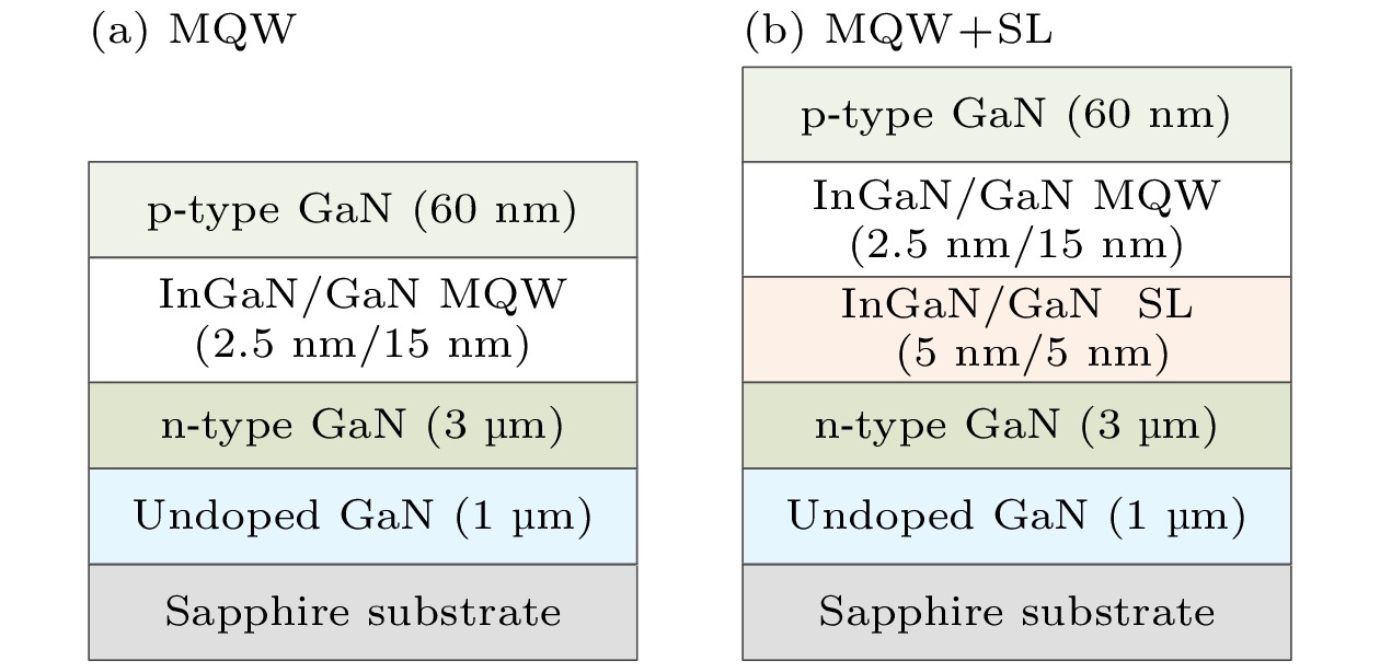
图 1 器件外延结构示意图 (a) 传统MQW结构; (b) 超晶格应变层MQW结构
Figure 1. Schematic diagram of the device epitaxial structure: (a) Traditional MQW structure; (b) MQW structure with a superlattice interlayer.
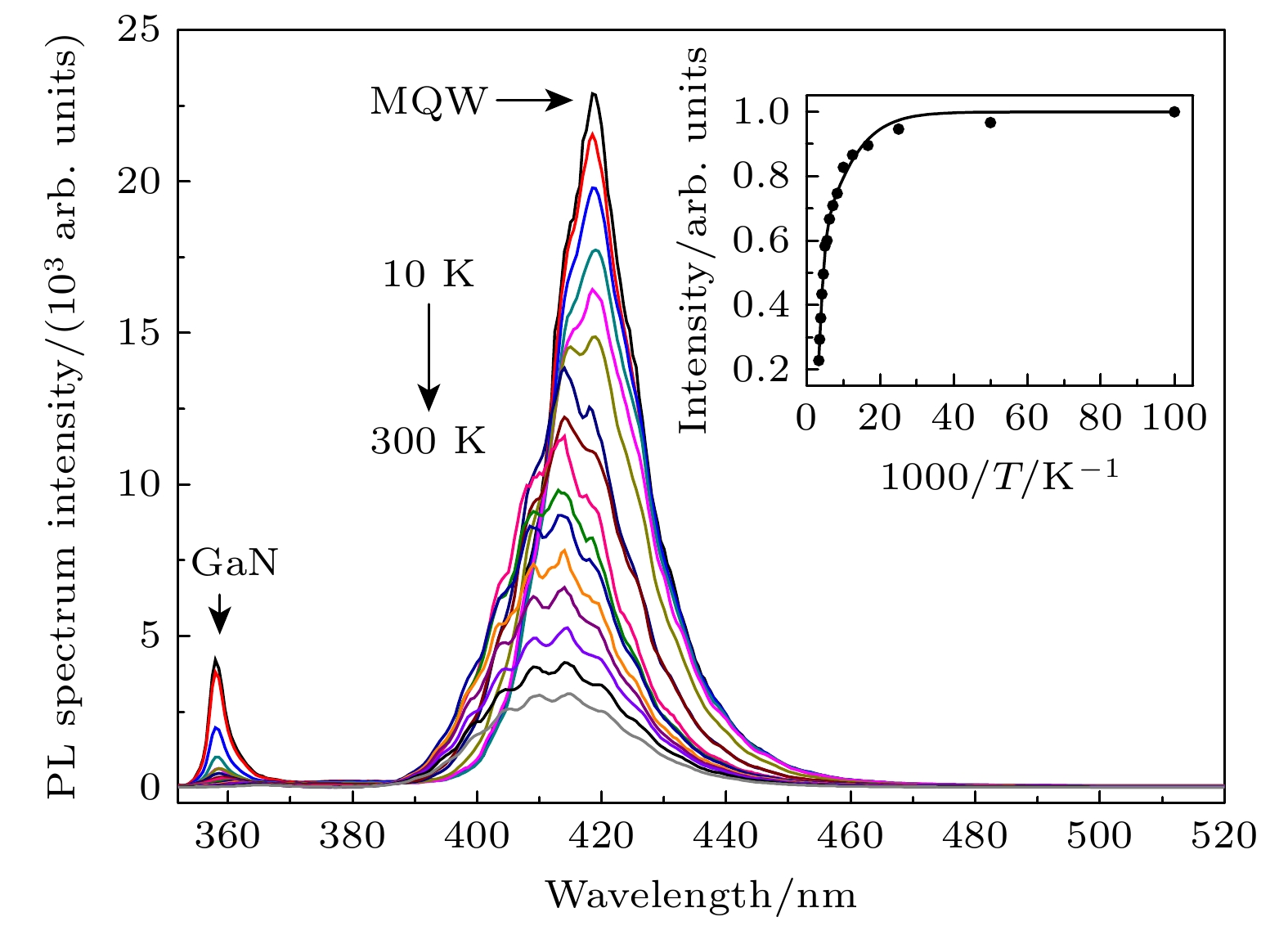
图 2 传统MQW结构在不同温度下的光致发光谱. 插图为PL谱积分强度随温度的变化及Arrhenius拟合曲线
Figure 2. PL spectra of the traditional MQW structure at different temperatures. The inset shows the temperature dependence of the integrated PL intensity with the best fitting of the Arrhenius plot.

图 3 超晶格应变层MQW结构在不同温度下的光致发光谱. 插图为PL谱积分强度随温度的变化及Arrhenius拟合曲线
Figure 3. PL spectra of the MQW structure with a SL interlayer at different temperatures. The inset shows the temperature dependence of the integrated PL intensity with the best fitting of the Arrhenius plot.

图 4 两种MQW结构PL谱峰值能量随温度的变化
Figure 4. Temperature-dependent variations of PL spectral peak energy for two MQW structures.

图 5 注入电流为100 mA时两种MQW结构的电致发光谱
Figure 5. EL spectra of two MQW structures at injection current of 100 mA.

图 6 注入电流为100 mA时两种样品的能带结构
Figure 6. Energy band diagrams of two samples at injection current of 100 mA.

图 7 注入电流为100 mA时, MQW结构(a)和超晶格应变层MQW结构(b)五个量子阱中电子空穴波函数空间分布和交叠
Figure 7. Electron and hole wave function distributions and overlaps in the five quantum wells of the MQW structure (a) and MQW structure with a SL interlayer (b) at 100 mA.
表 1 拟合参数α, β, EA1, EA2及内量子效率
Table 1. Fitting Parameters of α, β, EA1, and EA2 together with the internal quantum efficiency.
Sample IQE/% $ \alpha $ $ \beta $ $ {E_{{\text{A1}}}}{\text{/meV}} $ $ {E_{{\text{A2}}}}{\text{/meV}} $ MQW 22 0.33 9.28 5.36 47.80 MQW+SL 26 0.34 8.23 2.05 33.37  DownLoad: CSV
表 2 量子阱中电场强度和波函数交叠积分模拟结果
Table 2. Simulation results of the electric field and wave function overlaps in each quantum well.
MQW Electric field E1/(kV⋅cm–1) Overlap/% MQW+SL Electric field E2/(kV⋅cm–1) Overlap/% QW1 442.5 83.9 QW1 396.7 89.1 QW2 467.1 82.7 QW2 410.0 88.7 QW3 473.0 82.6 QW3 414.3 88.7 QW4 475.8 82.5 QW4 418.1 88.6 QW5 484.2 81.2 QW5 425.6 87.8
DownLoad: CSV
-
[1] Han D, Kim J, Shin D, Shim J 2023 Opt. Express 31 15779
Google Scholar
[2] Jeong H, Jeong H, Oh H, Hong C, Suh E, Lerondel G, Jeong M 2015 Sci. Rep. 5 9373
Google Scholar
[3] Zhou S, Wan Z, Lei Y, Tang B, Tao G, Du P, Zhao X 2022 Opt. Lett. 47 1291
Google Scholar
[4] Wu Y, Xiao Y, Navid I, Sun K, Malhotra Y, Wang P, Wang D, Xu Y, Pandey A, Reddeppa M, Shin W, Liu J, Min J, Mi Z 2022 Light Sci. Appl. 11 294
Google Scholar
[5] Das S, Lenka T, Talukdar F, Sadaf S, Velpula R, Nguyen H 2022 Appl. Opt. 61 8951
Google Scholar
[6] Cho L, Lee B, Lee K, Kim J, Ryu M 2021 J. Nanosci. Nanotechnol. 21 5648
Google Scholar
[7] Hu H, Zhou S, Wan H, Liu X, Li N, Xu H 2019 Sci. Rep. 9 3447
Google Scholar
[8] Li X, Liu J, Su X, Huang S, Tian A, Zhou W, Jiang L, Ikeda M, Yang H 2021 Materials (Basel, Switzerland) 14 1877
Google Scholar
[9] Cai J X, Sun H Q, Zheng H, Zhang P J, Guo Z Y 2014 Chin. Phys. B 23 58502
Google Scholar
[10] 邢艳辉, 邓军, 韩军, 李建军, 沈光池 2009 物理学报 58 590
Google Scholar
Xing Y H, Deng J, Han J, Li J J, Shen G C 2009 Acta Phys. Sin. 58 590
Google Scholar
[11] Shi J L, Shin Y C, Kim K C, Kim E H, Yun M S, Moon Y, Hwang S M, Kim T G 2008 J. Cryst. Growth 311 103
Google Scholar
[12] 齐维靖, 张萌, 潘拴, 王小兰, 张建立, 江风益 2016 物理学报 65 077801
Google Scholar
Qi W J, Zhang M, Pan S, Wang X L, Zhang J L, Jiang F Y 2016 Acta Phys. Sin. 65 077801
Google Scholar
[13] Cui S, Tao G, Gong L, Zhao X, Zhou S 2022 Materials (Basel, Switzerland) 15 8649
Google Scholar
[14] Liu L, Wang L, Li D, Liu N Y, Li L, Cao W Y, Yang W, Wan C H, Chen W H, Du W M, Hu X D, Feng Z C 2011 J. Appl. Phys. 109 073106
Google Scholar
[15] Chen C, Hsieh C, Liao C, Chung W, Chen H, Cao W, Chang W, Chen H, Yao Y, Ting S, Kiang Y, Yang C, Hu X 2012 Opt. Express 20 11321
Google Scholar
[16] Kuroda T, Tackeuchi A, Sota T 2000 Appl. Phys. Lett. 76 3753
Google Scholar
[17] Akasaka T, Gotoh H, Saito T, Makimoto T 2004 Appl. Phys. Lett. 85 3089
Google Scholar
[18] Kumano H, Hoshi K, Tanaka S, Suemune I, Shen X Q, Riblet P, Ramvall P, Aoyagi Y 1999 Appl. Phys. Lett. 75 2879
Google Scholar
[19] Ridley B K, Schaff W J, Eastman L F 2003 J. Appl. Phys. 94 3972
Google Scholar
[20] Sze S M, Ng K K 1981 Physics of Semiconductor Devices (New York: Wiley) p45
[21] Hsu L, Walukiewicz W 1998 Appl. Phys. Lett. 73 339
Google Scholar
[22] Fiorentini V, Bernardini F, Ambacher O 2002 Appl. Phys. Lett. 80 1204
Google Scholar
[23] Chuang S L 1995 Physics of Optoelectronic Devices (New York: Wiley) p560
[24] Zhang H, Miller E J, Yu E T, Poblenz C, Speck J S 2004 Appl. Phys. Lett. 84 4644
Google Scholar
[25] Renner F, Kiesel P, Döhler G H, Kneissl M, Van de Walle C G, Johnson N M 2002 Appl. Phys. Lett. 81 490
Google Scholar
[26] Braun W, Dowd P, Guo C Z, Chen S L, Ryu C M, Koelle U, Johnson S R, Zhang Y H, Tomm J W, Elsässer T, Smith D J 2000 J. Appl. Phys. 88 3004
Google Scholar

 DownLoad:
Catalog
Metrics
- Abstract views: 471
- PDF Downloads: 21
- Cited By: 0
