-
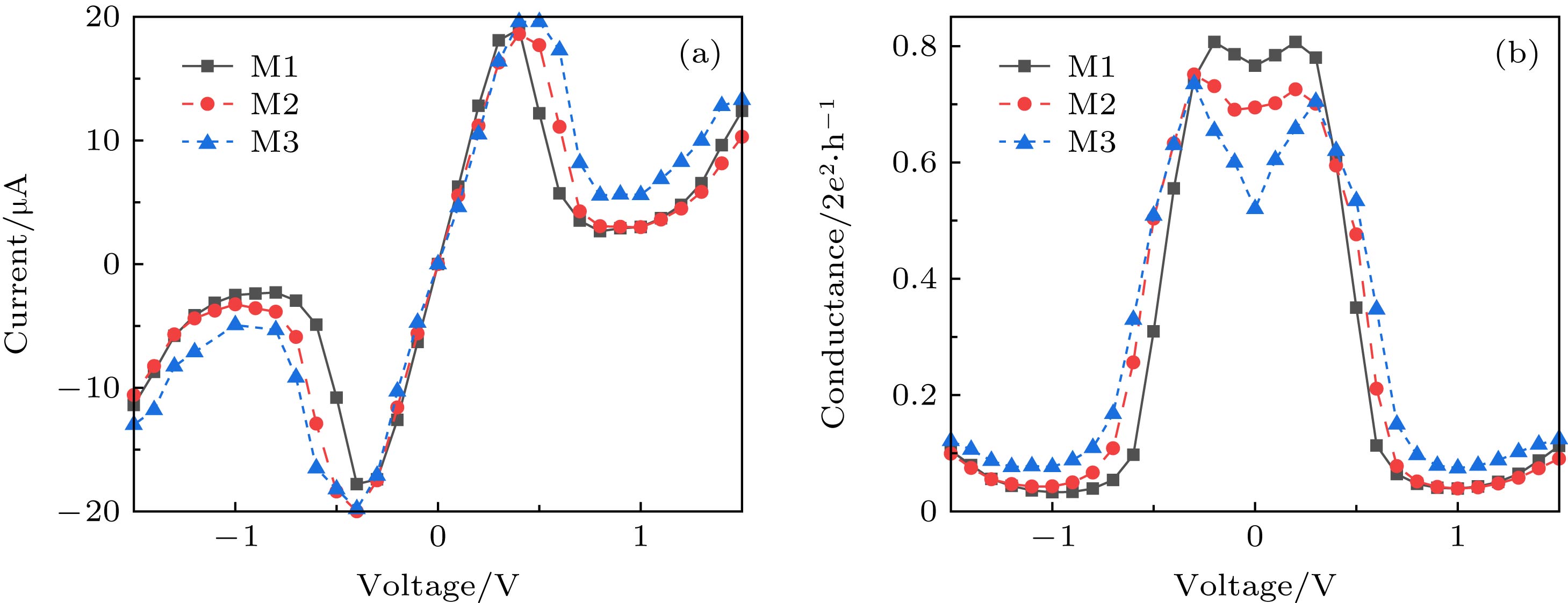
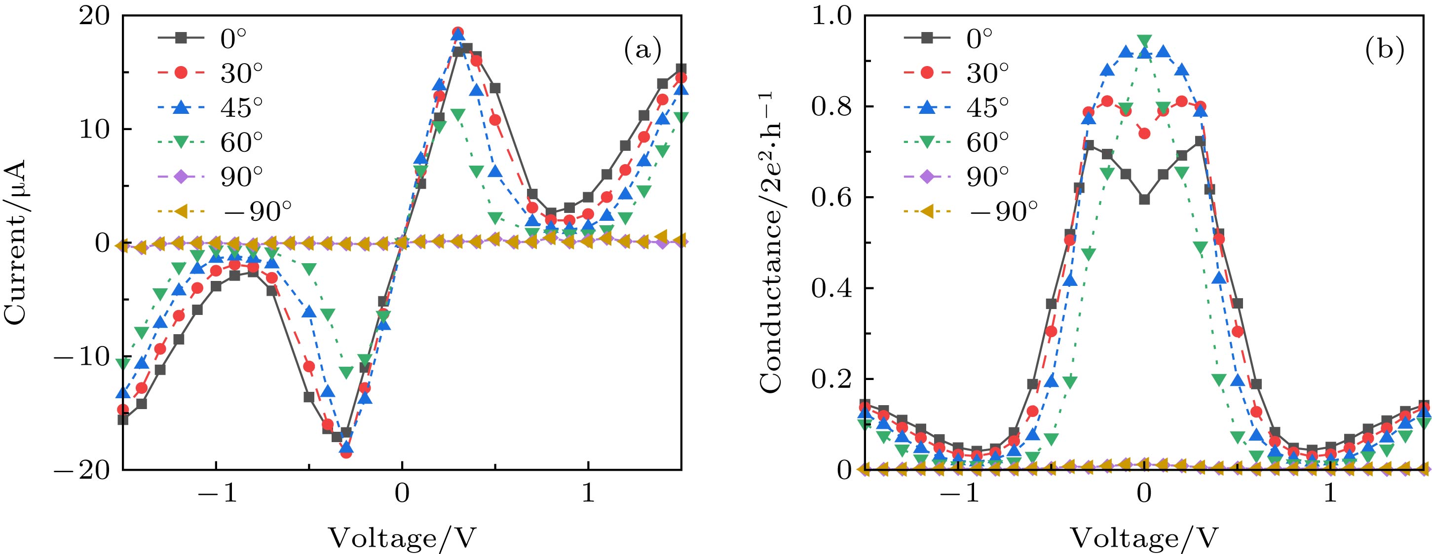
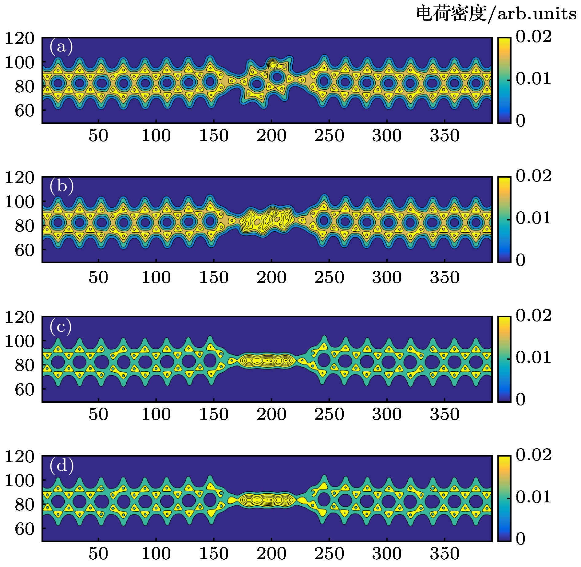
基于密度泛函理论与非平衡格林函数相结合的第一性原理计算方法, 系统地研究了通过碳原子(C)连接的同分异构喹啉分子(C9H5N)嵌于石墨烯纳米带电极间的分子电子器件输运性质. 研究结果表明: 器件电流在偏压[–0.3 V, +0.3 V]范围内呈线性变化, 电流在[–0.4 V, –0.9 V]和[+0.5 V, +0.8 V]范围内随着偏压的增大而减小, 呈现显著的负微分电阻效应; 当喹啉分子平面与石墨烯纳米带电极间存在一定夹角时, 器件电流呈现明显的负微分电阻效应且与喹啉分子平面旋转方向无关, 当喹啉分子平面与石墨烯纳米带电极垂直时, 器件电流截止. 以上研究结果得到偏压窗内透射系数积分以及零偏压下实空间电荷密度分布等的有力印证, 可为设计制作基于同分异构喹啉分子电子开关和负微分电阻器件提供理论依据.Since graphene was successfully obtained in the end of 2004, the research on graphene and relevant devices has attracted extensive attention. The armchair- and zigzag-edge graphene nanoribbons, as the building blocks, are often used to design the graphene-based molecular electronic devices. Quinoline, an important intermediate between metallurgical dyes and polymers, is an organic conjugated small molecule which is simple in structure and easy to synthesize and modify the chemical structure, and quinoline has become one of the research focuses in the field of molecular electronic devices in recent years. From the physical point of view, the transport properties of the isomeric quinoline molecular electronic devices connected with graphene nanoribbon electrodes can provide a theoretical basis for designing and manufacturing molecular electronic devices with excellent performance. Based on the first-principles calculation method combining the density functional theory and non-equilibrium Green's function, this paper systematically investigates the transport properties of the carbon-linked isomeric quinoline molecule electronic devices sandwiched between the graphene nanoribbon electrodes. The obtained results show that the device current presents a linear change in a bias voltage range [–0.3 V, +0.3 V], the current decreases with the increase of the absolute bias voltage, separately, in a range of [+0.5 V, +0.8 V] and [–0.4 V, –0.9 V], demonstrating a strong negative differential resistance effect. On the other hand, the interesting negative differential resistance effect is remained when there is an angle between the quinoline molecular plane and the graphene nanoribbon electrode; the current of the device is found to be independent of the rotation direction of quinoline molecule in the central region; the current of the device should be forbidden when the quinoline molecule plane is rotated to a direction vertical to the graphene nanoribbon electrodes. The obtained results can provide a theoretical basis for designing and manufacturing the molecular switches and negative differential resistance devices based on isomeric quinoline molecular electronic devices.
-
Keywords:
- isomeric quinoline molecule /
- graphene nanoribbon /
- first-principles calculation /
- electron transport
[1] Gimzewski J K, Joachim C 1999 Science 283 1683
 Google Scholar
[2] Aviram A 1989 Angew. Chem. 101 536
 Google Scholar
[3] Zhao P, Fang C, Xia C, Wang Y, Liu D, Xie S 2008 Appl. Phys. Lett. 93 013113
 Google Scholar
[4] Fu Q, Yang J, Luo Y 2009 Appl. Phys. Lett. 95 182103
 Google Scholar
[5] An Y P, Yang Z, Ratner M A 2011 J. Chem. Phys. 135 044706
 Google Scholar
[6] Fan Z Q, Zhang Z H, Deng X Q, Tang G P, Chen K Q 2012 Org. Electron. 13 2954
 Google Scholar
[7] Pan J, Zhang Z, Deng X, Qiu M, Guo C 2010 Appl. Phys. Lett. 97 203104
 Google Scholar
[8] Zeng J, Chen K Q, He J, Fan Z Q, Zhang X J 2011 J. Appl. Phys. 109 124502
 Google Scholar
[9] Wu Q H, Zhao P, Liu D S 2014 Acta Phys. Chim. Sin. 30 53
[10] Ren H, Li Q X, Luo Y, Yang J 2009 Appl. Phys. Lett. 94 173110
 Google Scholar
[11] Geng H, Hu Y, Shuai Z, Xia K, Gao H, Chen K 2007 J. Phys. Chem. C 111 19098
 Google Scholar
[12] Zhang J J, Zhang Z H, Guo C, Li J, Deng X Q 2012 Acta Phys. Chim. Sin. 28 1701
[13] Zhang X, Chen K, Long M, He J, Gao Y 2015 Mod. Phys. Lett. B 29 1550106
 Google Scholar
[14] Ozaki T, Nishio K, Weng H, Kino H 2010 Phys. Rev. B 81 075422
 Google Scholar
[15] Zhang D, Long M, Zhang X, Ouyang F, Li M, Xu H 2015 J. Appl. Phys. 117 014311
 Google Scholar
[16] Cui L L, Long M Q, Zhang X J, Li X M, Zhang D, Yang B C 2016 Phys. Lett. A 380 730
 Google Scholar
[17] Jia C, Migliore A, Xin N, Huang S, Wang J, Yang Q, Wang S, Chen H, Wang D, Feng B 2016 Science 352 1443
 Google Scholar
[18] Wen H M, Yang Y, Zhou X S, Liu J Y, Zhang D B, Chen Z B, Wang J Y, Chen Z N, Tian Z Q 2013 Chem. Sci. 4 2471
 Google Scholar
[19] Metzger R M 2003 Chem. Rev. 103 3803
 Google Scholar
[20] Chung A, Deen J, Lee J S, Meyyappan M 2010 Nanotechnology 21 412001
 Google Scholar
[21] Chen J, Reed M, Rawlett A, Tour J 1999 Science 286 1550
 Google Scholar
[22] Joachim C, Gimzewski J K, Schlittler R R, Chavy C 1995 Phys. Rev. Lett. 74 2102
 Google Scholar
[23] Wan H, Zhou B, Chen X, Sun C Q, Zhou G 2012 J. Phys. Chem. C 116 2570
 Google Scholar
[24] Danilov A V, Hedegård P, Golubev D S, Bjørnholm T, Kubatkin S E 2008 Nano Lett. 8 2393
 Google Scholar
[25] Bumm L, Arnold J, Cygan M, Dunbar T, Burgin T, Jones L, Allara D L, Tour J M, Weiss P 1996 Science 271 1705
 Google Scholar
[26] Reed M A, Zhou C, Muller C, Burgin T, Tour J 1997 Science 278 252
 Google Scholar
[27] Chen J, Wang W, Reed M, Rawlett A, Price D, Tour J 2000 Appl. Phys. Lett. 77 1224
 Google Scholar
[28] Venkataraman L, Klare J E, Nuckolls C, Hybertsen M S, Steigerwald M L 2006 Nature 442 904
 Google Scholar
[29] Quinn J R, Foss Jr F W, Venkataraman L, Hybertsen M S, Breslow R 2007 J. Am. Chem. Soc. 129 6714
 Google Scholar
[30] Fu W, Xu Z, Bai X, Gu C, Wang E 2009 Nano Lett. 9 921
 Google Scholar
[31] Wang J, Zhu M, Outlaw R, Zhao X, Manos D, Holloway B, Mammana V 2004 Appl. Phys. Lett. 85 1265
 Google Scholar
[32] Lin Z, Jun W 2014 Chin. Phys. B 23 087202
 Google Scholar
[33] Novoselov K S, Geim A K, Morozov S V, Jiang D, Zhang Y, Dubonos S V, Grigorieva I V, Firsov A A 2004 Science 306 666
 Google Scholar
[34] 王雪梅, 刘红 2011 物理学报 60 047102
 Google Scholar
Wang X M, Liu H 2011 Acta Phys. Sin. 60 047102
 Google Scholar
[35] Li X, Wang X, Zhang L, Lee S, Dai H 2008 Science 319 1229
 Google Scholar
[36] Son Y W, Cohen M L, Louie S G 2006 Nature 444 347
 Google Scholar
[37] Wen B, Cao M S, Lu M M, Cao W Q, Shi H G, Liu J, Wang X X, Jin H B, Fang X Y, Wang W Z 2014 Adv. Mater. 26 3484
 Google Scholar
[38] Cao M S, Shu J C, Wang X X, Wang X, Zhang M, Yang H J, Fang X Y, Yuan J 2019 Annalen Der Physik 531 1800390
 Google Scholar
[39] Cao M S, Wang X X, Zhang M, Shu J C, Cao W Q, Yang H J, Fang X Y, Yuan J 2019 Adv. Funct. Mater. 29 1807398
 Google Scholar
[40] Zhang M, Wang X X, Cao W Q, Yuan J, Cao M S 2019 Adv. Opt. Mater. 4 1900689
[41] Fang X Y, Yu X X, Zheng H M, Jin H B, Wang L, Cao M S 2015 Phys. Lett. A 379 2245
 Google Scholar
[42] Cao M S, Wang X X, Cao W Q, Fang X Y, Wen B, Yuan J 2018 Small 14 1800987
 Google Scholar
[43] Cao W Q, Wang X X, Yuan J, Wang W Z, Cao M S 2015 J. Mater. Chem. C 3 10017
 Google Scholar
[44] Wen B, Cao M S, Hou Z L, Song W L, Zhang L, Lu M M, Jin H B, Fang X Y, Wang W Z, Yuan J 2013 Carbon 65 124
 Google Scholar
[45] Taylor J, Guo H, Wang J 2001 Phys. Rev. B 63 245407
 Google Scholar
[46] Taylor J, Guo H, Wang J 2001 Phys. Rev. B 63 121104
 Google Scholar
[47] Waldron D, Haney P, Larade B, MacDonald A, Guo H 2006 Phys. Rev. Lett. 96 166804
 Google Scholar
[48] Waldron D, Timoshevskii V, Hu Y, Xia K, Guo H 2006 Phys. Rev. Lett. 97 226802
 Google Scholar
[49] Perdew J P, Zunger A 1981 Phys. Rev. B 23 5048
 Google Scholar
[50] Copple A, Ralston N, Peng X 2012 Appl. Phys. Lett. 100 193108
 Google Scholar
[51] Brandbyge M, Mozos J L, Ordejón P, Taylor J, Stokbro K 2002 Phys. Rev. B 65 165401
 Google Scholar
[52] Lee C, Yang W, Parr R G 1988 Phys. Rev. B 37 785
 Google Scholar
[53] Perdew J P, Burke K, Ernzerhof M 1996 Phys. Rev. Lett. 77 3865
 Google Scholar
[54] Hammer B, Hansen L, Nørskov J 1999 Phys. Rev. B 59 7413
 Google Scholar
[55] Guo B, Liu Q, Chen E, Zhu H, Fang L, Gong J R 2010 Nano Lett. 10 4975
 Google Scholar
[56] Datta S 1997 Electronic Transport in Mesoscopic Systems (2nd ed.) (The United Kingdom: Cambridge University Press) pp102−112
-
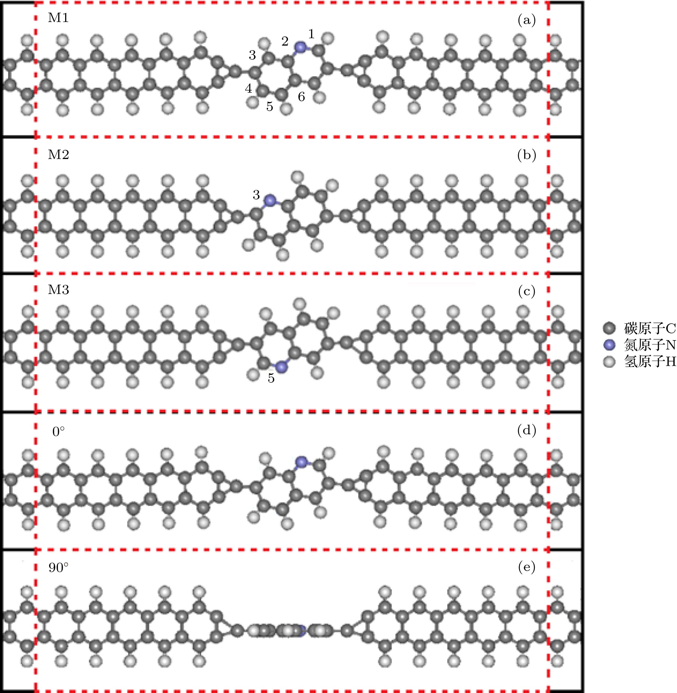
图 1 由半无限长锯齿型石墨烯纳米带左电极/中心散射区/半无限长锯齿型石墨烯纳米带右电极组成的ZGNR/C9H5N/ZGNR分子电子器件结构示意图, 红色方框区域表示中心散射区 (a)—(c)分别对应喹啉C9H5N分子中氮原子N处于编号2, 3和5处; (d)和(e)给出喹啉C9H5N分子平面与石墨烯纳米带电极平面成0°和90°时的模型
Fig. 1. ZGNR/C9H5N/ZGNR molecular electronic device schematic diagram consisted of a semi-infinite ZGNR left electrode/a central scattering region/a semi-infinite right ZGNR electrode, the red dashed line area represents the central scattering region. (a)−(c) denotes the marked 2nd, 3rd and 5th N atom of the C9H5N molecular; (d) and (e) illustrates the model of the 0° and 90° angle between the C9H5N molecule and graphene nanoribbon electrodes, respectively.
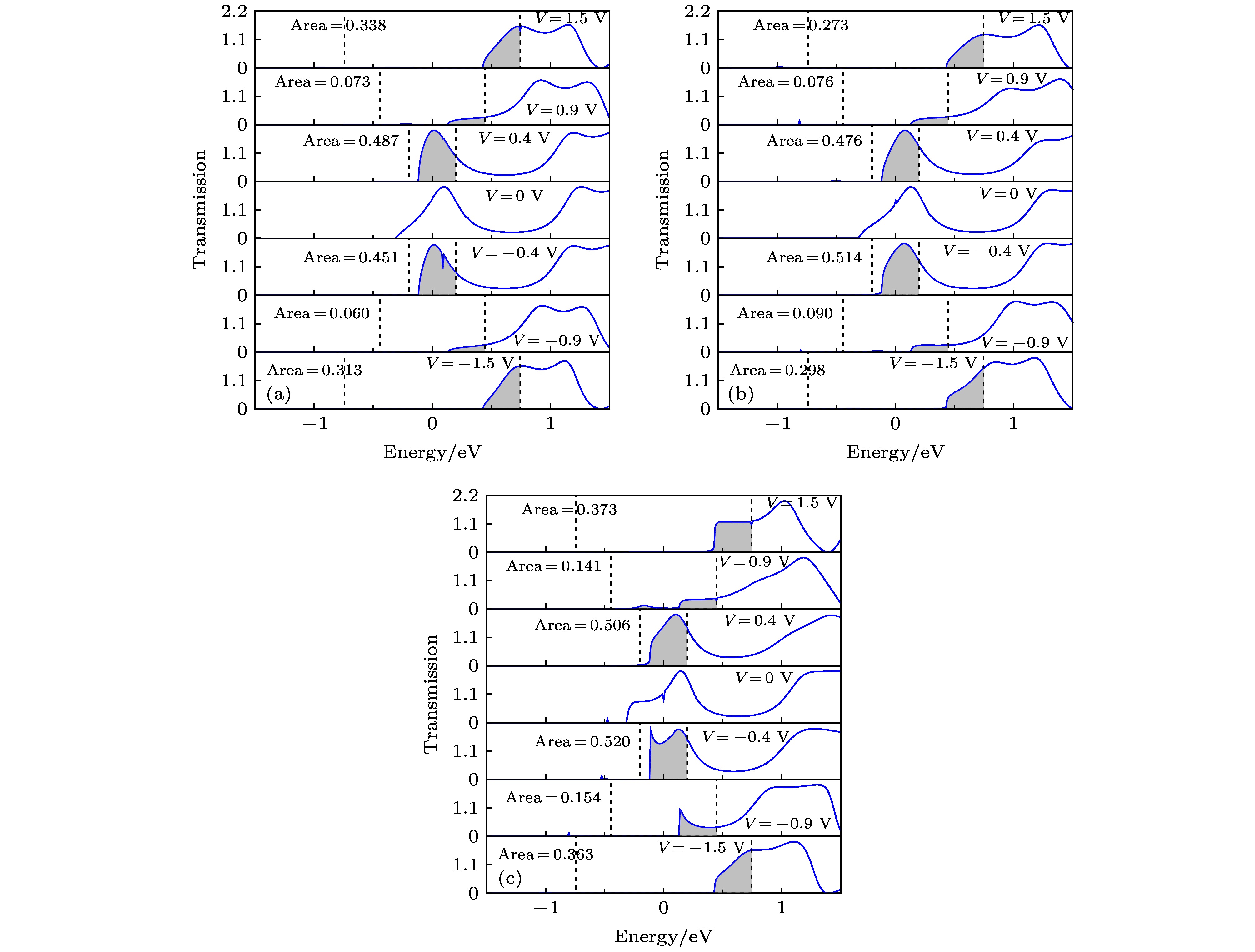
图 3 器件(a) M1、(b) M2和(c) M3在0, ±0.4 V, ±0.9 V以及±1.5 V偏压下的透射谱, 图中的黑色虚线和阴影部分面积分别表示偏压窗和偏压窗内的透射系数积分面积
Fig. 3. The transmission spectrum of the device (a) M1, (b) M2 and (c) M3 under the bias voltage of 0, ±0.4 V, ±0.9 V and ±1.5 V, where the (black) dashed lines and shaded area denote the bias window and the integrated area of the transmission coefficient in the bias window, respectively.
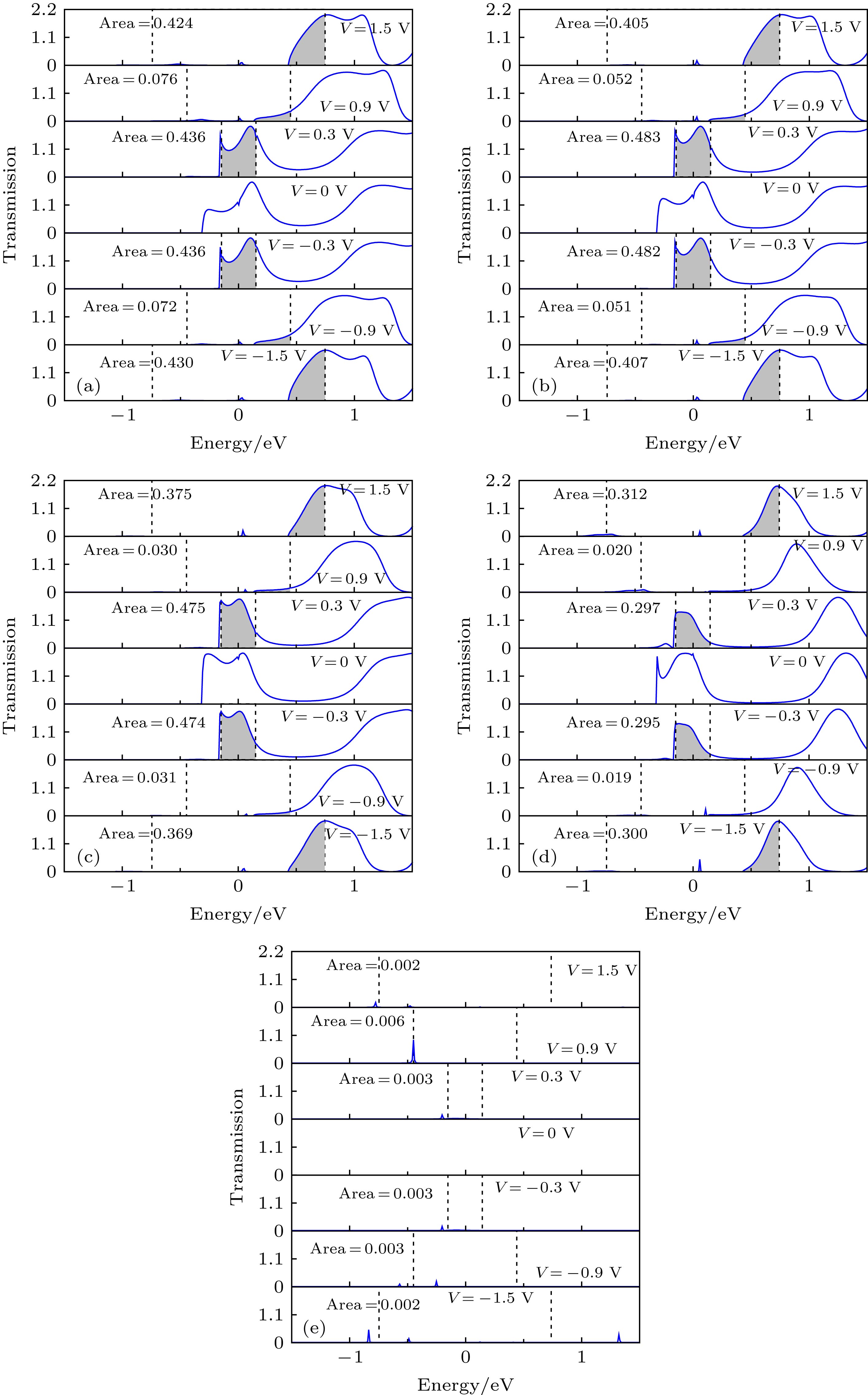
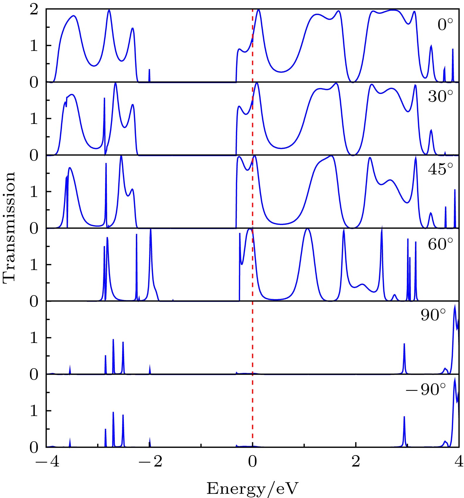
图 5 偏压0, ± 0.3 V, ± 0.9 V以及 ± 1.5 V下喹啉C9H5N分子平面与石墨烯纳米带电极分别成 (a) 0°, (b) 30°, (c) 45°, (d) 60°和(e) 90°时的透射谱, 图中的黑色虚线和阴影部分面积分别表示偏压窗和偏压窗内透射系数积分面积
Fig. 5. The transmission spectra for the angle between the C9H5N molecules and graphene nanoribbon electrodes is (a) 0°, (b) 30°, (c) 45°, (d) 60° and (e) 90°, respectively, under the bias voltage of 0, ± 0.3 V, ± 0.9 V and ± 1.5 V, where the (black) dashed lines and shaded area denote the bias window and the integrated area of the transmission coefficient in the bias window, respectively.
-
[1] Gimzewski J K, Joachim C 1999 Science 283 1683
 Google Scholar
[2] Aviram A 1989 Angew. Chem. 101 536
 Google Scholar
[3] Zhao P, Fang C, Xia C, Wang Y, Liu D, Xie S 2008 Appl. Phys. Lett. 93 013113
 Google Scholar
[4] Fu Q, Yang J, Luo Y 2009 Appl. Phys. Lett. 95 182103
 Google Scholar
[5] An Y P, Yang Z, Ratner M A 2011 J. Chem. Phys. 135 044706
 Google Scholar
[6] Fan Z Q, Zhang Z H, Deng X Q, Tang G P, Chen K Q 2012 Org. Electron. 13 2954
 Google Scholar
[7] Pan J, Zhang Z, Deng X, Qiu M, Guo C 2010 Appl. Phys. Lett. 97 203104
 Google Scholar
[8] Zeng J, Chen K Q, He J, Fan Z Q, Zhang X J 2011 J. Appl. Phys. 109 124502
 Google Scholar
[9] Wu Q H, Zhao P, Liu D S 2014 Acta Phys. Chim. Sin. 30 53
[10] Ren H, Li Q X, Luo Y, Yang J 2009 Appl. Phys. Lett. 94 173110
 Google Scholar
[11] Geng H, Hu Y, Shuai Z, Xia K, Gao H, Chen K 2007 J. Phys. Chem. C 111 19098
 Google Scholar
[12] Zhang J J, Zhang Z H, Guo C, Li J, Deng X Q 2012 Acta Phys. Chim. Sin. 28 1701
[13] Zhang X, Chen K, Long M, He J, Gao Y 2015 Mod. Phys. Lett. B 29 1550106
 Google Scholar
[14] Ozaki T, Nishio K, Weng H, Kino H 2010 Phys. Rev. B 81 075422
 Google Scholar
[15] Zhang D, Long M, Zhang X, Ouyang F, Li M, Xu H 2015 J. Appl. Phys. 117 014311
 Google Scholar
[16] Cui L L, Long M Q, Zhang X J, Li X M, Zhang D, Yang B C 2016 Phys. Lett. A 380 730
 Google Scholar
[17] Jia C, Migliore A, Xin N, Huang S, Wang J, Yang Q, Wang S, Chen H, Wang D, Feng B 2016 Science 352 1443
 Google Scholar
[18] Wen H M, Yang Y, Zhou X S, Liu J Y, Zhang D B, Chen Z B, Wang J Y, Chen Z N, Tian Z Q 2013 Chem. Sci. 4 2471
 Google Scholar
[19] Metzger R M 2003 Chem. Rev. 103 3803
 Google Scholar
[20] Chung A, Deen J, Lee J S, Meyyappan M 2010 Nanotechnology 21 412001
 Google Scholar
[21] Chen J, Reed M, Rawlett A, Tour J 1999 Science 286 1550
 Google Scholar
[22] Joachim C, Gimzewski J K, Schlittler R R, Chavy C 1995 Phys. Rev. Lett. 74 2102
 Google Scholar
[23] Wan H, Zhou B, Chen X, Sun C Q, Zhou G 2012 J. Phys. Chem. C 116 2570
 Google Scholar
[24] Danilov A V, Hedegård P, Golubev D S, Bjørnholm T, Kubatkin S E 2008 Nano Lett. 8 2393
 Google Scholar
[25] Bumm L, Arnold J, Cygan M, Dunbar T, Burgin T, Jones L, Allara D L, Tour J M, Weiss P 1996 Science 271 1705
 Google Scholar
[26] Reed M A, Zhou C, Muller C, Burgin T, Tour J 1997 Science 278 252
 Google Scholar
[27] Chen J, Wang W, Reed M, Rawlett A, Price D, Tour J 2000 Appl. Phys. Lett. 77 1224
 Google Scholar
[28] Venkataraman L, Klare J E, Nuckolls C, Hybertsen M S, Steigerwald M L 2006 Nature 442 904
 Google Scholar
[29] Quinn J R, Foss Jr F W, Venkataraman L, Hybertsen M S, Breslow R 2007 J. Am. Chem. Soc. 129 6714
 Google Scholar
[30] Fu W, Xu Z, Bai X, Gu C, Wang E 2009 Nano Lett. 9 921
 Google Scholar
[31] Wang J, Zhu M, Outlaw R, Zhao X, Manos D, Holloway B, Mammana V 2004 Appl. Phys. Lett. 85 1265
 Google Scholar
[32] Lin Z, Jun W 2014 Chin. Phys. B 23 087202
 Google Scholar
[33] Novoselov K S, Geim A K, Morozov S V, Jiang D, Zhang Y, Dubonos S V, Grigorieva I V, Firsov A A 2004 Science 306 666
 Google Scholar
[34] 王雪梅, 刘红 2011 物理学报 60 047102
 Google Scholar
Wang X M, Liu H 2011 Acta Phys. Sin. 60 047102
 Google Scholar
[35] Li X, Wang X, Zhang L, Lee S, Dai H 2008 Science 319 1229
 Google Scholar
[36] Son Y W, Cohen M L, Louie S G 2006 Nature 444 347
 Google Scholar
[37] Wen B, Cao M S, Lu M M, Cao W Q, Shi H G, Liu J, Wang X X, Jin H B, Fang X Y, Wang W Z 2014 Adv. Mater. 26 3484
 Google Scholar
[38] Cao M S, Shu J C, Wang X X, Wang X, Zhang M, Yang H J, Fang X Y, Yuan J 2019 Annalen Der Physik 531 1800390
 Google Scholar
[39] Cao M S, Wang X X, Zhang M, Shu J C, Cao W Q, Yang H J, Fang X Y, Yuan J 2019 Adv. Funct. Mater. 29 1807398
 Google Scholar
[40] Zhang M, Wang X X, Cao W Q, Yuan J, Cao M S 2019 Adv. Opt. Mater. 4 1900689
[41] Fang X Y, Yu X X, Zheng H M, Jin H B, Wang L, Cao M S 2015 Phys. Lett. A 379 2245
 Google Scholar
[42] Cao M S, Wang X X, Cao W Q, Fang X Y, Wen B, Yuan J 2018 Small 14 1800987
 Google Scholar
[43] Cao W Q, Wang X X, Yuan J, Wang W Z, Cao M S 2015 J. Mater. Chem. C 3 10017
 Google Scholar
[44] Wen B, Cao M S, Hou Z L, Song W L, Zhang L, Lu M M, Jin H B, Fang X Y, Wang W Z, Yuan J 2013 Carbon 65 124
 Google Scholar
[45] Taylor J, Guo H, Wang J 2001 Phys. Rev. B 63 245407
 Google Scholar
[46] Taylor J, Guo H, Wang J 2001 Phys. Rev. B 63 121104
 Google Scholar
[47] Waldron D, Haney P, Larade B, MacDonald A, Guo H 2006 Phys. Rev. Lett. 96 166804
 Google Scholar
[48] Waldron D, Timoshevskii V, Hu Y, Xia K, Guo H 2006 Phys. Rev. Lett. 97 226802
 Google Scholar
[49] Perdew J P, Zunger A 1981 Phys. Rev. B 23 5048
 Google Scholar
[50] Copple A, Ralston N, Peng X 2012 Appl. Phys. Lett. 100 193108
 Google Scholar
[51] Brandbyge M, Mozos J L, Ordejón P, Taylor J, Stokbro K 2002 Phys. Rev. B 65 165401
 Google Scholar
[52] Lee C, Yang W, Parr R G 1988 Phys. Rev. B 37 785
 Google Scholar
[53] Perdew J P, Burke K, Ernzerhof M 1996 Phys. Rev. Lett. 77 3865
 Google Scholar
[54] Hammer B, Hansen L, Nørskov J 1999 Phys. Rev. B 59 7413
 Google Scholar
[55] Guo B, Liu Q, Chen E, Zhu H, Fang L, Gong J R 2010 Nano Lett. 10 4975
 Google Scholar
[56] Datta S 1997 Electronic Transport in Mesoscopic Systems (2nd ed.) (The United Kingdom: Cambridge University Press) pp102−112
计量
- 文章访问数: 10793
- PDF下载量: 124
- 被引次数: 0


 下载:
下载:
