


-
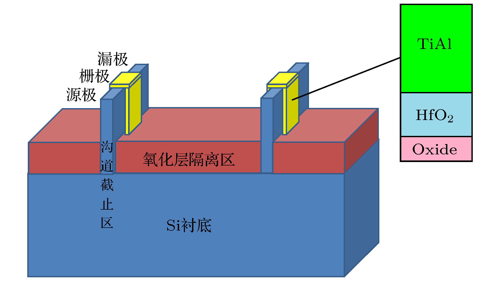
体硅鳍形场效应晶体管(FinFET)是晶体管尺寸缩小到30 nm以下应用最多的结构, 其单粒子瞬态产生机理值得关注. 利用脉冲激光单粒子效应模拟平台开展了栅长为30, 40, 60, 100 nm FinFET器件的单粒子瞬态实验, 研究FinFET器件单粒子瞬态电流脉冲波形随栅长变化情况; 利用计算机辅助设计(technology computer-aided design, TCAD)软件仿真比较电流脉冲产生过程中器件内部电子浓度和电势变化, 研究漏电流脉冲波形产生的物理机理. 研究表明, 不同栅长FinFET器件瞬态电流脉冲尾部都存在明显的平台区, 且平台区电流值随着栅长变短而增大; 入射激光在器件沟道区下方体区产生高浓度电子将源漏导通产生导通电流, 而源漏导通升高了体区电势, 抑制体区高浓度电子扩散, 使得导通状态维持时间长, 形成平台区电流; 尾部平台区由于持续时间长, 收集电荷量大, 会严重影响器件工作状态和性能. 研究结论为纳米FinFET器件抗辐射加固提供理论支撑.Fin field effect transistor (FinFET) is a most widely used structure when the field effect transistor is scaled down to 30 nm or less. And there are few studies on single-event transient of FinFET devices with gate length below 30 nm. The single-event-transient on FinFET with gate length below 30 nm is worth studying. The single-event-transient responses of bulk FinFETs with 30 nm, 40 nm, 60 nm and 100 nm gate length are examined by using the pulsed laser and technology computer-aided design (TCAD) simulation in this article. First, we use the pulsed laser to ionize the gate of the FinFET device and detect the transient drain current of the FinFET device. The experimental results show that there are obvious platforms for the transient drain current tails of FinFETs with different gate lengths, and the platform current increases as the gate length of FinFET becomes shorter. The charges collected in the platform of FinFET devices with gate lengths of 100, 60, 40, and 30 nm are 34%, 40%, 51%, and 65% of the total charge collected in transient drain current, respectively. Therefore, when the FinFET device with the gate length below 100 nm, the platform current will seriously affect the device performance. Second, we use TCAD to simulate the heavy ion single-event effect of FinFET device and study the generation mechanism of platform region in transient drain current. The TCAD simulation explains this mechanism. Laser or heavy ions ionize high concentration electron-hole pairs in the device. The holes are quickly collected and the high concentration electrons are left under the FinFET channel. High concentration electrons conduct source and drain, generating the source-to-drain current at the tail of the transient drain current. Moreover the source-drain conduction enhances the electrostatic potential below the FinFET channel and suppresses high-concentration electron diffusion, making source-to-drain current decrease slowly and form the platform. The transient drain current tail has a long duration and a large quantity of collected charges, which seriously affects FinFET performance. This is a problem that needs studying in the single-event effect of FinFET device. It is also a problem difficult to solve when the FinFET devices are applied to spacecraft. And the generation mechanism of the transient drain current plateau region of FinFET device can provide theoretical guidance for solving these problems.
-
Keywords:
- single-event transient /
- source-drain conduction /
- platform current
[1] Colinge J P 2008 FinFETs and Other Multi-Gate Transistors (New York: Springer) pp257–258
[2] Herman C H J, Michiel S M, van AHM Arthur R 2011 Analog Circuit Design-Robust Design, Sigma Delta Converters, RFID (New York: Springer) pp69–87
[3] Nsengiyumva P, Ball D R, Kauppila J S, Tam N, McCurdy M, Holman W T, Alles M L, Bhuva B L, Massengill L W 2016 IEEE Trans. Nucl. Sci. 63 266
 Google Scholar
[4] Nsengiyumva P, Massengill L W, Alles M L, Bhuva B L, Ball D R, Kauppila J S, Haeffner T D, Holman W T, Reed R A 2017 IEEE Trans. Nucl. Sci. 64 441
Google Scholar
[5] Zhang H F, Jiang H, Assis T R, et al. 2017 IEEE Trans. Nucl. Sci. 64 457
Google Scholar
[6] Nsengiyumva P, Massengill L W, Kauppila J S, Maharrey J A, Harrington R C, Haeffner T D, Ball D R, Alles M L, Bhuva B L, Holman W T, Zhang E X, Rowe J D, Sternberg A L 2018 IEEE Trans. Nucl. Sci. 65 223
Google Scholar
[7] Narasimham B, Hatami S, Anvar A, Harris D M, Lin A, Wang J K, Chatterjee I, Ni K, Bhuva B L, Schrimpf R D, Reed R A, McCurdy M W 2015 IEEE Trans. Nucl. Sci. 62 2578
Google Scholar
[8] Harrington R C, Maharrey J A, Kauppila J S, Nsengiyumva P, Ball D R, Haeffner T D, Zhang E X, Bhuva B L, Massengill L W 2018 IEEE Trans. Nucl. Sci. 65 1807
Google Scholar
[9] Karp J, Hart M J, Maillard P, Hellings G, Linten D 2018 IEEE Trans. Nucl. Sci. 65 217
Google Scholar
[10] Gong H Q, Ni K, Zhang E X, Sternberg A L, Kozub J A, Ryder K L, Keller R F, Ryder L D, Weiss S M, Weller R A, Alles M L, Reed R A, Fleetwood D M, Schrimpf R D, Vardi A, Jesús A 2018 IEEE Trans. Nucl. Sci. 65 296
Google Scholar
[11] Gong H Q, Ni K, Zhang E X, Sternberg A L, Kozub J A, Alles M L, Reed R A, Fleetwood D M, Schrimpf R D, Waldron N, Kunert B, Linten D 2019 IEEE Trans. Nucl. Sci. 66 376
Google Scholar
[12] Ni K, Sternberg A L, Zhang E X, Kozub J A, Rong J, Schrimpf R D, Reed R A, Fleetwood D M, Alles M L, McMorrow D, Lin J Q, Vardi A, Jesús A 2017 IEEE Trans. Nucl. Sci. 64 2069
Google Scholar
[13] El-Mamouni F, Zhang E X, Pate N D, Hooten N, Schrimpf R D, Reed R A, Galloway K F, McMorrow D, Warner J, Simoen E, Claeys C, Griffoni A, Linten D, Vizkelethy G 2011 IEEE Trans. Nucl. Sci. 58 2563
Google Scholar
[14] El-Mamouni F, Zhang E X, Ball D R, Sierawski B, King M P, Schrimpf R D, Reed R A, Alles M L, Fleetwood D M, Linten D, Simoen E, Vizkelethy G 2012 IEEE Trans. Nucl. Sci. 59 2674
Google Scholar
[15] 于俊庭 2017 博士学位论文 (长沙: 国防科技大学)
Yu J T 2017 Ph. D. Dissertation (Changsha: National University of Defense Technology) (in Chinese)
[16] Yu J T, Chen S M, Chen J J, Huang P C, Song R Q 2016 Chin. Phys. B 25 049401
Google Scholar
[17] Yu J T, Chen S M, Chen J J, Huang P C 2015 Chin. Phys. B 24 119401
Google Scholar
[18] Wu Z Y, Zhu B N, Yi T Y, Li C, Liu Y, Yang Y T 2018 J. Comput. Electron. 17 1608
Google Scholar
[19] Li G S, An X, Ren Z X, Wang J N, Huang R 2018 IEEE International Conference on Solid-State and Integrated Circuit Technology (ICSICT) Qingdao, China, Oct. 31–Nov. 3, 2018 p1
[20] 田恺, 曹洲, 薛玉雄, 杨世宇 2010 原子能科学技术 44 489
Tian K, Cao Z, Xue Y X, Yang S Y 2010 At. Energ. Sci. Technol. 44 489
[21] 黄建国, 韩建伟 2004 中国科学G辑: 物理学 力学 天文学 34 601
Haung J G, Han J W 2004 Science in China Series G: Physics, Mechanics & Astronomy 34 601
[22] Adams J H 1983 IEEE Trans. Nucl. Sci. 30 4475
Google Scholar
[23] 卓青青, 刘红侠, 郝跃 2012 物理学报 61 218501
Google Scholar
Zhuo Q Q, Liu H X, Hao Y 2012 Acta Phys. Sin. 61 218501
Google Scholar
-

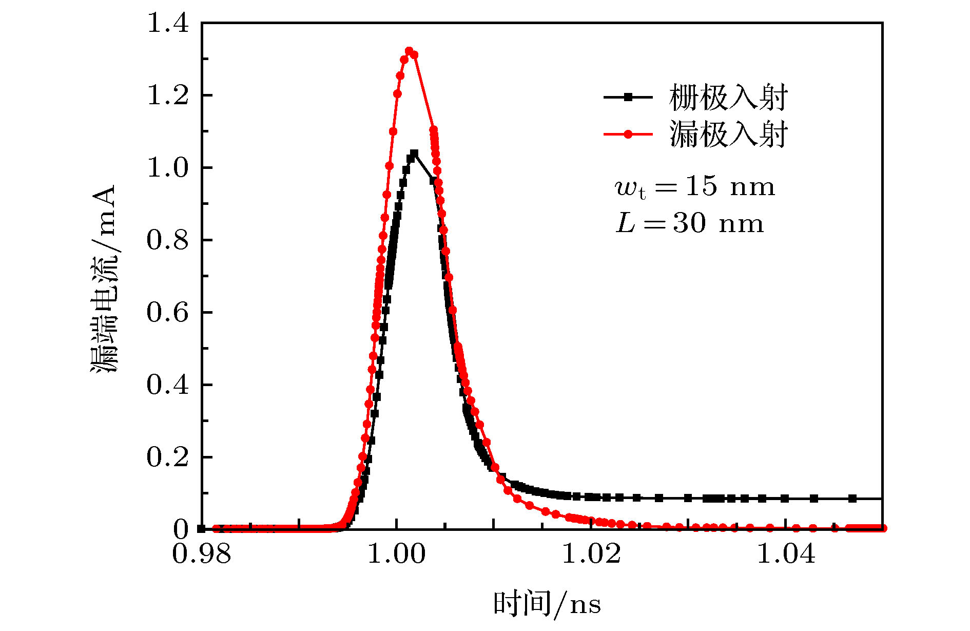
图 3 4鳍不同栅长FinFET器件在5 nJ激光照射下的漏电流脉冲
Fig. 3. Drain current transients for 4 fin FinFET of different gate length during the 5 nJ laser testing.
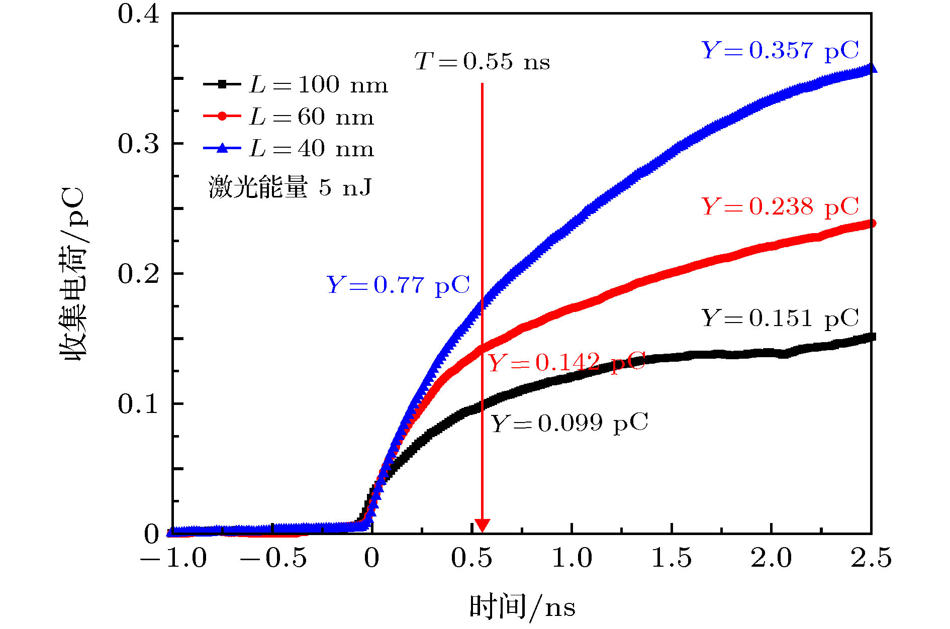
图 4 4鳍不同栅长器件在5 nJ激光入射下漏端收集电荷与时间关系
Fig. 4. Drain charge collected for 4 fin FinFET of different gate length during the 5 nJ laser testing as a function of time.
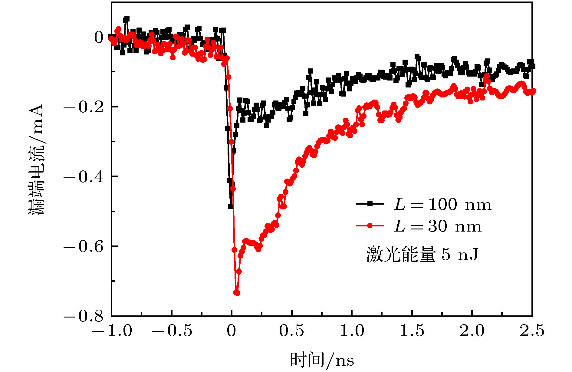
图 5 双鳍 100和30 nm栅长器件在5 nJ激光入射下漏电流脉冲
Fig. 5. Drain current transients for 2 fin FinFET of different gate length during the 5 nJ laser testing.
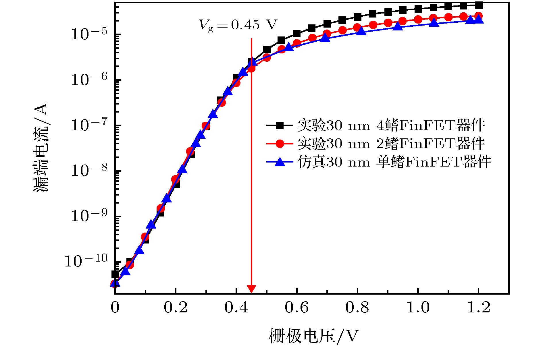
图 6 单鳍FinFET仿真器件和2鳍、4鳍FinFET实验器件
$ I_{\rm d}\text{-}V_{\rm g} $ 曲线Fig. 6.
$ I_{\rm d}\text{-}V_{\rm g} $ for simulation single-fin FinFET and experimental 2 and 4 fins FinFET.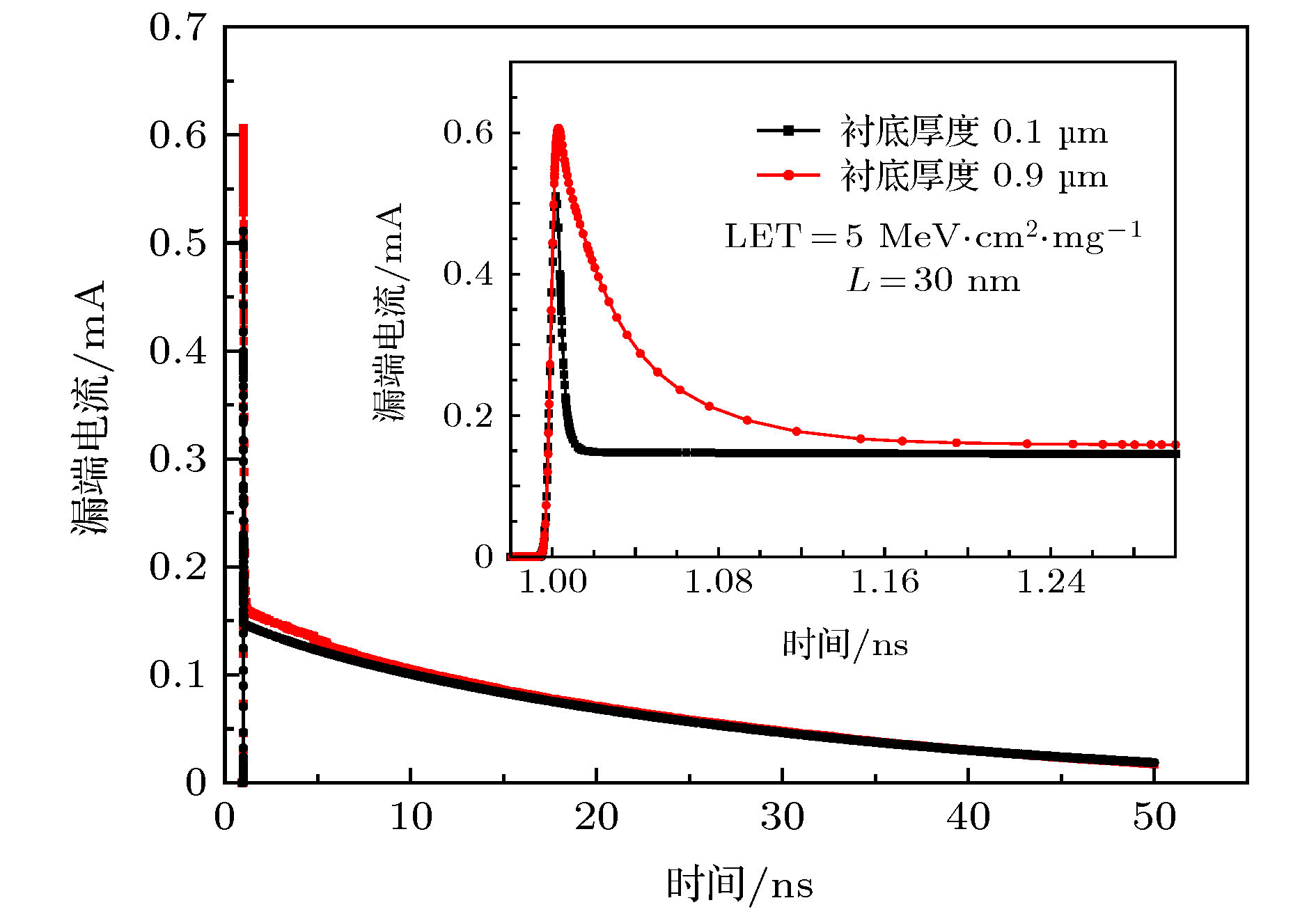
图 7 TCAD模拟下衬底厚度为0.1和0.9 μm, 栅长为30 nm FinFET器件漏电流脉冲
Fig. 7. Drain current transients for FinFET of different substrate thickness from TCAD simulation.
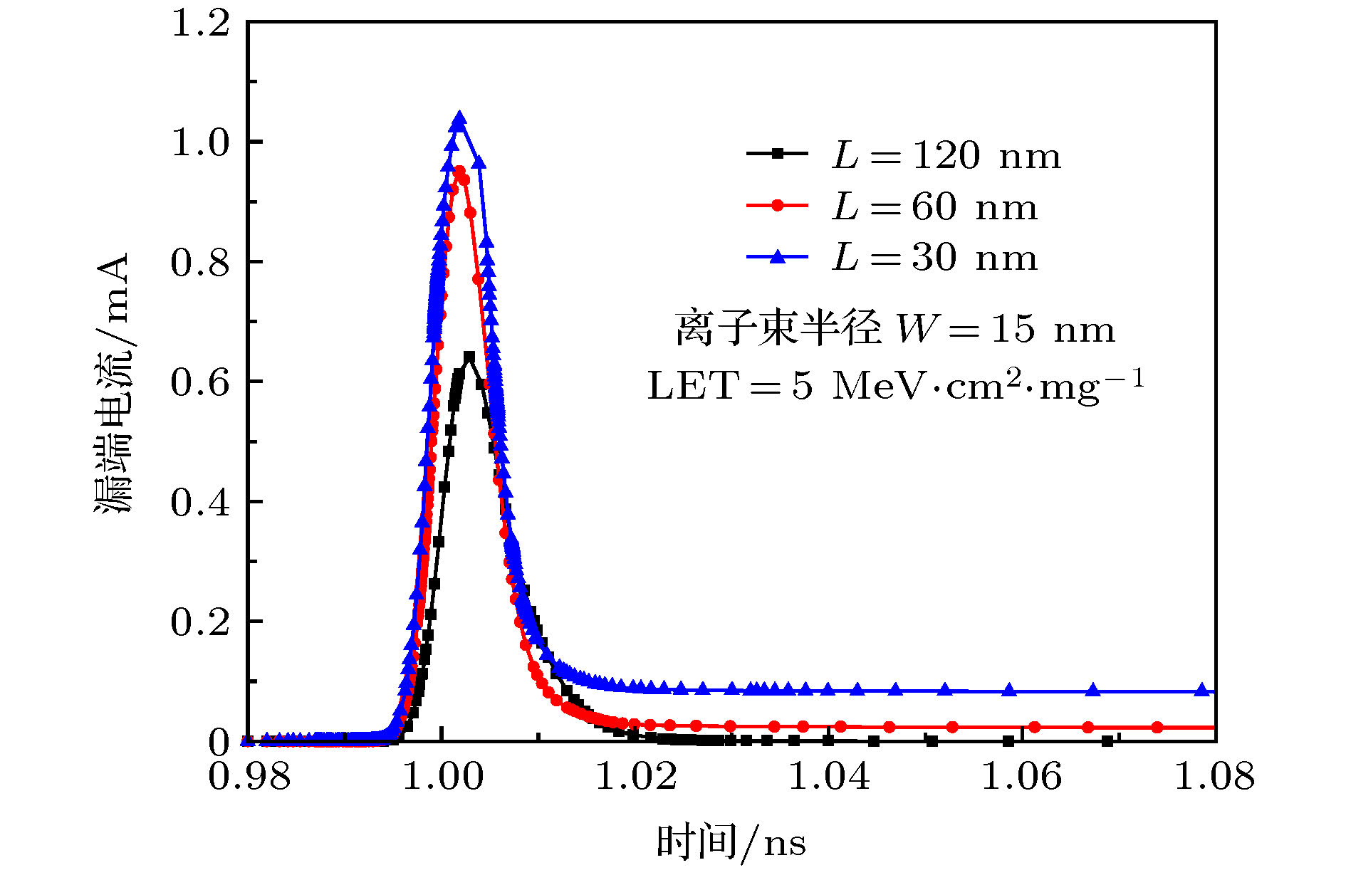
图 8 TCAD模拟下不同栅长FinFET器件漏电流脉冲
Fig. 8. Drain current transients for FinFET of different gate length from TCAD simulation.
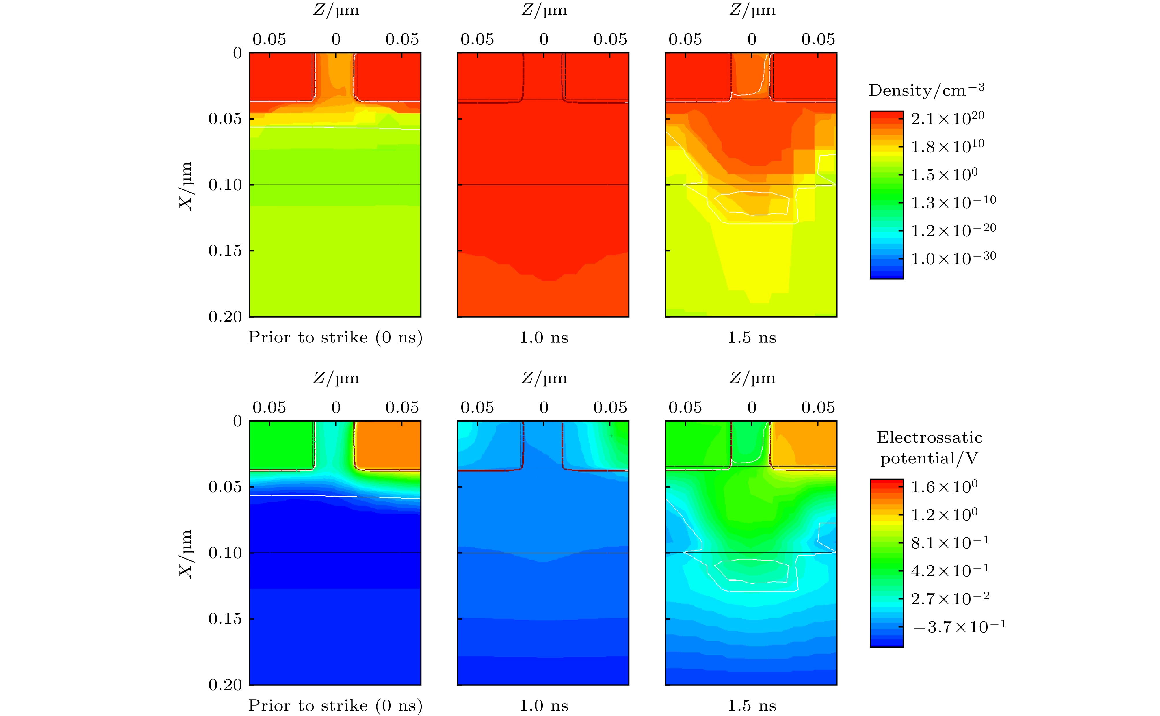
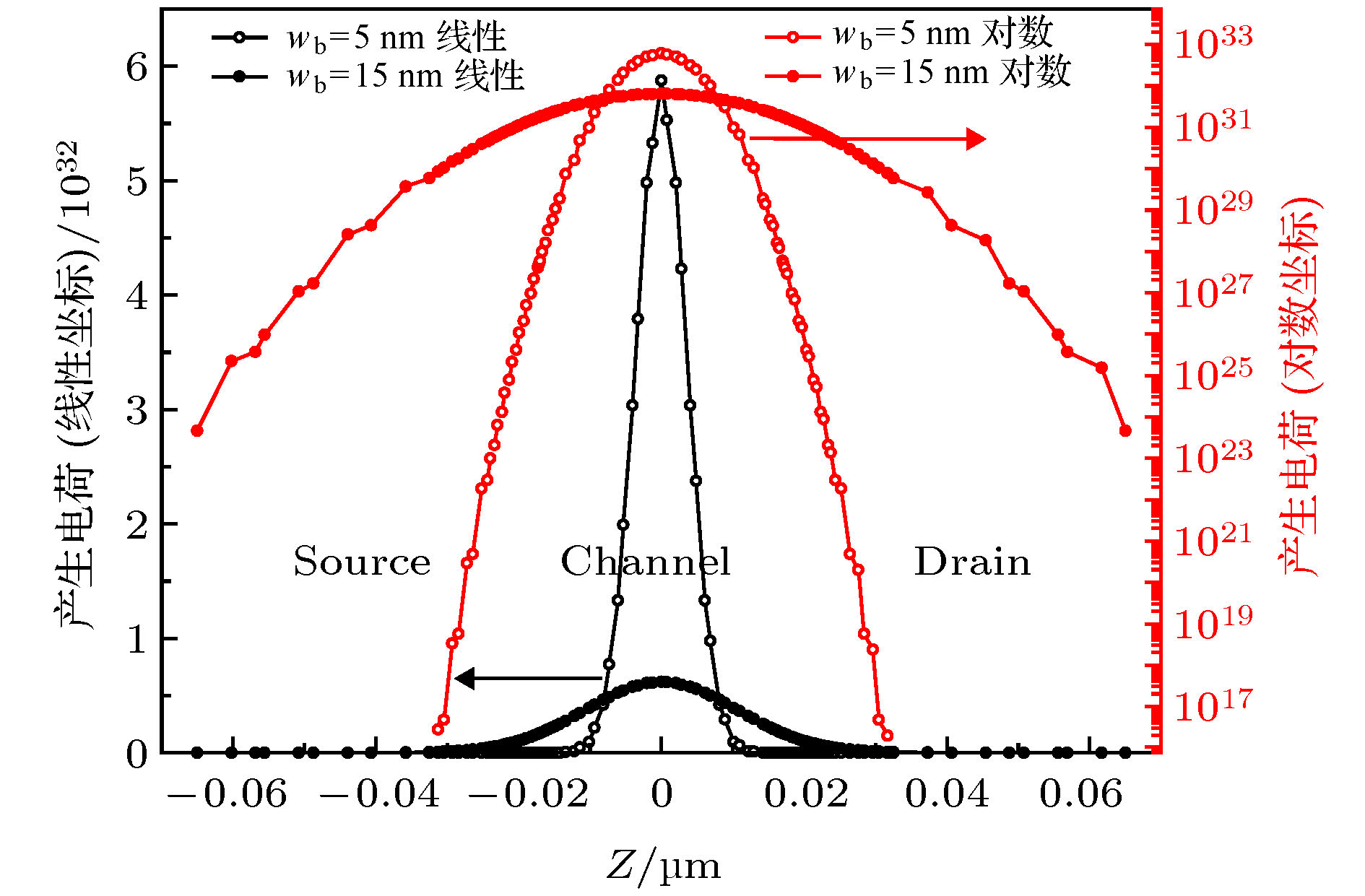
图 10 重离子入射前、入射中和入射后30 nm FinFET器件内部电子浓度和电势分布
Fig. 10. Temporary evolution of electronic density and electrostatic potential for a 30 nm FinFET.
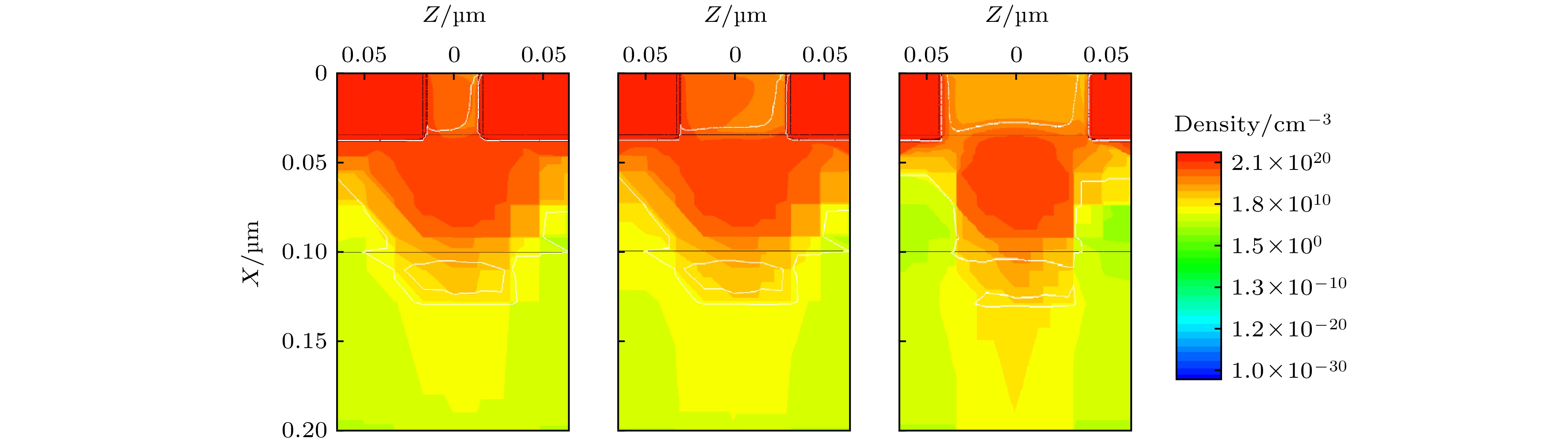
图 11 不同栅长FinFET器件在1.5 ns时的电子浓度
Fig. 11. Electronic density for FinFET of different gate length at 1.5 ns.
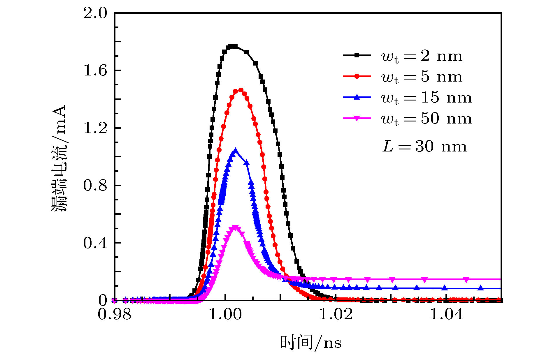
图 12 30 nm器件在不同特征半径重离子入射下漏电流脉冲
Fig. 12. Drain current transient for 30 nm FinFET when heavy ion incident device with different radius.
-
[1] Colinge J P 2008 FinFETs and Other Multi-Gate Transistors (New York: Springer) pp257–258
[2] Herman C H J, Michiel S M, van AHM Arthur R 2011 Analog Circuit Design-Robust Design, Sigma Delta Converters, RFID (New York: Springer) pp69–87
[3] Nsengiyumva P, Ball D R, Kauppila J S, Tam N, McCurdy M, Holman W T, Alles M L, Bhuva B L, Massengill L W 2016 IEEE Trans. Nucl. Sci. 63 266
Google Scholar
[4] Nsengiyumva P, Massengill L W, Alles M L, Bhuva B L, Ball D R, Kauppila J S, Haeffner T D, Holman W T, Reed R A 2017 IEEE Trans. Nucl. Sci. 64 441
Google Scholar
[5] Zhang H F, Jiang H, Assis T R, et al. 2017 IEEE Trans. Nucl. Sci. 64 457
Google Scholar
[6] Nsengiyumva P, Massengill L W, Kauppila J S, Maharrey J A, Harrington R C, Haeffner T D, Ball D R, Alles M L, Bhuva B L, Holman W T, Zhang E X, Rowe J D, Sternberg A L 2018 IEEE Trans. Nucl. Sci. 65 223
Google Scholar
[7] Narasimham B, Hatami S, Anvar A, Harris D M, Lin A, Wang J K, Chatterjee I, Ni K, Bhuva B L, Schrimpf R D, Reed R A, McCurdy M W 2015 IEEE Trans. Nucl. Sci. 62 2578
Google Scholar
[8] Harrington R C, Maharrey J A, Kauppila J S, Nsengiyumva P, Ball D R, Haeffner T D, Zhang E X, Bhuva B L, Massengill L W 2018 IEEE Trans. Nucl. Sci. 65 1807
Google Scholar
[9] Karp J, Hart M J, Maillard P, Hellings G, Linten D 2018 IEEE Trans. Nucl. Sci. 65 217
Google Scholar
[10] Gong H Q, Ni K, Zhang E X, Sternberg A L, Kozub J A, Ryder K L, Keller R F, Ryder L D, Weiss S M, Weller R A, Alles M L, Reed R A, Fleetwood D M, Schrimpf R D, Vardi A, Jesús A 2018 IEEE Trans. Nucl. Sci. 65 296
Google Scholar
[11] Gong H Q, Ni K, Zhang E X, Sternberg A L, Kozub J A, Alles M L, Reed R A, Fleetwood D M, Schrimpf R D, Waldron N, Kunert B, Linten D 2019 IEEE Trans. Nucl. Sci. 66 376
Google Scholar
[12] Ni K, Sternberg A L, Zhang E X, Kozub J A, Rong J, Schrimpf R D, Reed R A, Fleetwood D M, Alles M L, McMorrow D, Lin J Q, Vardi A, Jesús A 2017 IEEE Trans. Nucl. Sci. 64 2069
Google Scholar
[13] El-Mamouni F, Zhang E X, Pate N D, Hooten N, Schrimpf R D, Reed R A, Galloway K F, McMorrow D, Warner J, Simoen E, Claeys C, Griffoni A, Linten D, Vizkelethy G 2011 IEEE Trans. Nucl. Sci. 58 2563
Google Scholar
[14] El-Mamouni F, Zhang E X, Ball D R, Sierawski B, King M P, Schrimpf R D, Reed R A, Alles M L, Fleetwood D M, Linten D, Simoen E, Vizkelethy G 2012 IEEE Trans. Nucl. Sci. 59 2674
Google Scholar
[15] 于俊庭 2017 博士学位论文 (长沙: 国防科技大学)
Yu J T 2017 Ph. D. Dissertation (Changsha: National University of Defense Technology) (in Chinese)
[16] Yu J T, Chen S M, Chen J J, Huang P C, Song R Q 2016 Chin. Phys. B 25 049401
Google Scholar
[17] Yu J T, Chen S M, Chen J J, Huang P C 2015 Chin. Phys. B 24 119401
Google Scholar
[18] Wu Z Y, Zhu B N, Yi T Y, Li C, Liu Y, Yang Y T 2018 J. Comput. Electron. 17 1608
Google Scholar
[19] Li G S, An X, Ren Z X, Wang J N, Huang R 2018 IEEE International Conference on Solid-State and Integrated Circuit Technology (ICSICT) Qingdao, China, Oct. 31–Nov. 3, 2018 p1
[20] 田恺, 曹洲, 薛玉雄, 杨世宇 2010 原子能科学技术 44 489
Tian K, Cao Z, Xue Y X, Yang S Y 2010 At. Energ. Sci. Technol. 44 489
[21] 黄建国, 韩建伟 2004 中国科学G辑: 物理学 力学 天文学 34 601
Haung J G, Han J W 2004 Science in China Series G: Physics, Mechanics & Astronomy 34 601
[22] Adams J H 1983 IEEE Trans. Nucl. Sci. 30 4475
Google Scholar
[23] 卓青青, 刘红侠, 郝跃 2012 物理学报 61 218501
Google Scholar
Zhuo Q Q, Liu H X, Hao Y 2012 Acta Phys. Sin. 61 218501
Google Scholar

 下载:
下载:


计量
- 文章访问数: 13091
- PDF下载量: 104
- 被引次数: 0
