


-
为了使具备光和电注入AlGaAs/GaAs 负电子亲和势(NEA)阵列阴极获得较高的发射电流效率, 基于变带隙发射阵列中电子输运的二维连续性方程, 利用有限体积法进行数值求解和仿真, 得到发射电流和发射电流效率. 通过仿真得到既适合光注入又合适电注入的各层最佳参数范围. 结果表明, 选择占空比为2/3的阵列微纳米柱, 获得光注入阴极的最佳入射光角度范围为10°—30°; 光注入(电注入)情况下P型变带隙AlGaAs层阵列微纳米柱高度范围为0.3—0.6 μm (0.1—0.3 μm), N型变带隙AlGaAs层、N型AlGaAs层以及P型AlGaAs层最佳厚度范围分别为0.5—2.5 μm (2—3 μm), 0.5—1.0 μm (0.8—1.2 μm)和0.2—0.5 μm (0.1—0.3 μm); P型AlGaAs层和N型AlGaAs层最佳掺杂浓度范围分别为5×10¹⁸—1×1019 cm–3 (1×10¹⁸—5×1018 cm–3)和1×10¹⁸—5×1018 cm–3 (5×10¹⁷—1×1018 cm–3). 光注入下发射电流效率最大为35.04%, 单位长度最大发射电流为10.3 nA/μm; 电注入下发射电流效率最大为31.23%, 单位长度最大发射电流105.5 μA/μm.In order to obtain high emission current efficiency of the AlGaAs/GaAs NEA array cathode, this array cathode has two ways to form electron emission, i.e. optical injection and electrical injection. The two-dimensional continuity equation of electronic transport in the variable bandgap emission array is solved numerically by using the finite volume method thereby obtaining the emission current and emission current efficiency. Simulation obtains the optimal parameter range for each layer of the AlGaAs/GaAs NEA array cathode under both optical injection and electrical injection. The results show that the optimal angle of incident light for the array cathode under light injection is 10°–30° for selecting an array micro-nano column with a duty cycle of 2/3. Under the condition of light injection, the P-type variable bandgap AlGaAs layer array micro-nano column height ranges from 0.3–0.6 μm. Under the condition of electrical injection, the height of the micro-nano column of the P-type variable bandgap AlGaAs layer array is 0.1–0.3 μm. The optimal thickness range of N-type variable bandgap AlGaAs layer, N-type AlGaAs layer, and P-type AlGaAs layer under light injection are 0.5–2.5 μm, 0.5–1.0 μm and 0.2–0.5 μm, respectively. The optimal thickness range of N-type variable bandgap AlGaAs layer, N-type AlGaAs layer, and P-type AlGaAs layer under electrical injection conditions are 2–3 μm, 0.8–1.2 μm and 0.1–0.3 μm, respectively. The optimal doping concentration of P-type AlGaAs layer and N-type AlGaAs layer under light injection are range from 5×10¹⁸ to 1×1019 cm–3 and from 1×10¹⁸ to 5×1018 cm–3, respectively. The optimal doping concentration of the P-type AlGaAs layer and the N-type AlGaAs layer under electrical injection range from 1×10¹⁸ to 5×1018 cm–3 and from 5×10¹⁷ to 1×1018 cm–3, respectively. The maximum efficiency of the emission current under the light injection is 35.04%, and the maximum emission current per unit length is 10.3 nA/μm. The maximum efficiency of the emission current under electrical injection is 31.23%, and the maximum emission current per unit length is 105.5 μA/μm. Electric injection cathode does not need expensive and complex drive laser system, and the light injection control mode is simple, so light injection or electrical injection control mode can be chosen as needed. The research of array cathode, which integrates the advantages of many advanced technologies, is of great significance for enriching the cathode array cathode emission theory and expanding its application field.
-
Keywords:
- light injection /
- electric injection /
- arrays cathode /
- emission current efficiency
[1] Tsentalovich E, Barkhuff D, Chen J, Dodson G, Farkhondeh M, Franklin W, Ihloff E, Kaertner F, Tschalaer C, Yang B, Zwart T 2007 Nucl. Instrum. Methods Phys. Res., Sect. A 582 413
 Google Scholar
[2] Benson S V, Douglas D, Neil G R, Shinn M D 2011 J. Phys. Conf. Ser. 299 012014
Google Scholar
[3] Liu W, Chen Y Q, Lu W T, Moy A, Poelker M, Stutzman M, Zhang S K 2016 Appl. Phys. Lett. 109 252104
Google Scholar
[4] Yamamoto N, Yamamoto M, Kuwahara M, Sakai R, Morino T, Tamagaki K, Mano A, Utsu A, Okumi S, Nakanishi T, Kuriki M, Bo C, Ujihara T, Takeda Y 2007 J. Appl. Phys. 102 024904
Google Scholar
[5] Pierce D T, Meier F 1976 Phys. Rev. B 13 5484
Google Scholar
[6] 滕利华, 牟丽君 2017 物理学报 66 046802
Google Scholar
Teng L H, Mu L J 2017 Acta Phys. Sin. 66 046802
Google Scholar
[7] Su C Y, Spicer W E, Lindau I 1983 J. Appl. Phys. 54 1413
Google Scholar
[8] Cultrera L, Galdi A, Bae J K, Ikponmwen F, Maxson J, Bazarov I 2020 Phys. Rev. Accel. Beams 23 023401
Google Scholar
[9] Machuca F, Liu Z, Sun Y, Pianetta P, Spicer W E, Pease R F W 2003 J. Vac. Sci. Technol. B 21 1863
Google Scholar
[10] Maruyama T, Brachmann A, Clendenin J E, Desikan T, Garwin E L, Kirby R E, Luh D A, Turner J, Prepost R 2002 Nucl. Instrum. Methods Phys. Res. Sect. A 492 199
Google Scholar
[11] 李晓峰 2001 博士学位论文 (西安: 中国科学院西安光学精密机械研究所)
Li X F 2001 Ph. D. Dissertation (Xi’an: Xi’an Institute of Optical and Precision Mechanics, Chinese Academy of Sciences) (in Chinese)
[12] Zhang Q, Bai X F, Cheng H C, Jiao G C, Li Z K, Han K, Li Q 2022 Acta Photonica Sin. 51 0304005
Google Scholar
[13] Liu L, Lu F F, Tian J, Zhangyang X Y, Lv Z S 2020 J. Mater. Sci. Technol. 58 86
Google Scholar
[14] 邓文娟, 彭新村, 邹继军, 江少涛, 郭栋, 张益军, 常本康 2014 物理学报 63 167902
Google Scholar
Deng W J, Peng X C, Zou J J, Jiang S T, Guo D, Zhang Y J, Chang B K 2014 Acta Phys. Sin. 63 167902
Google Scholar
[15] 邹继军, 高频, 杨智, 常本康 2008 光子学报 37 1112
Zou J J, Gao P, Yang Z, Chang B K 2008 Acta Photonica Sin. 37 1112
[16] Xia S, Liu L, Kong Y K 2016 Opt. Quantum Electron. 48 306
Google Scholar
[17] 张涛 2018 电子世界 15 65
Zhang T 2018 Electron. World 15 65
[18] 曾梦丝, 彭新村 2018 光学仪器 40 67
Zeng M S, Peng X C 2018 Opt. Instrum. 40 67
[19] 邹继军, 张益军, 杨智, 常本康 2011 物理学报 60 017902
Google Scholar
Zou J J, Zhang Y J, Yang Z, Chang B K 2011 Acta Phys. Sin. 60 017902
Google Scholar
[20] Xia J Y, Zou J J, Peng X C, Deng W J, Zhang Y J 2020 Ultramicroscopy 219 113121
Google Scholar
[21] Ding X J, Ge X W, Zou J J, Zhang Y J, Peng X C, Deng W J, Chen Z P, Zhao W J, Chang B K 2016 Opt. Commun. 367 149
Google Scholar
-

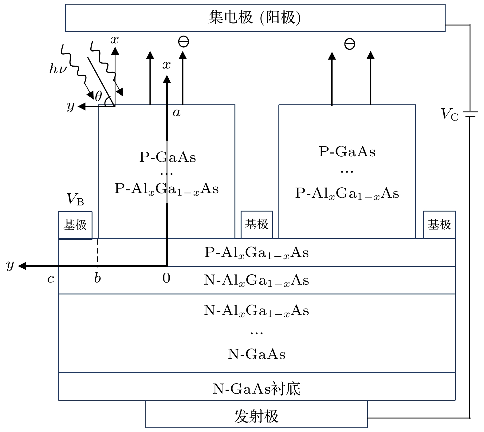
图 2 光和电注入NEA阵列阴极光电发射过程和能带结构图
Fig. 2. Photoelectric emission process and band structure diagram of the light and electrical injection NEA array cathode.
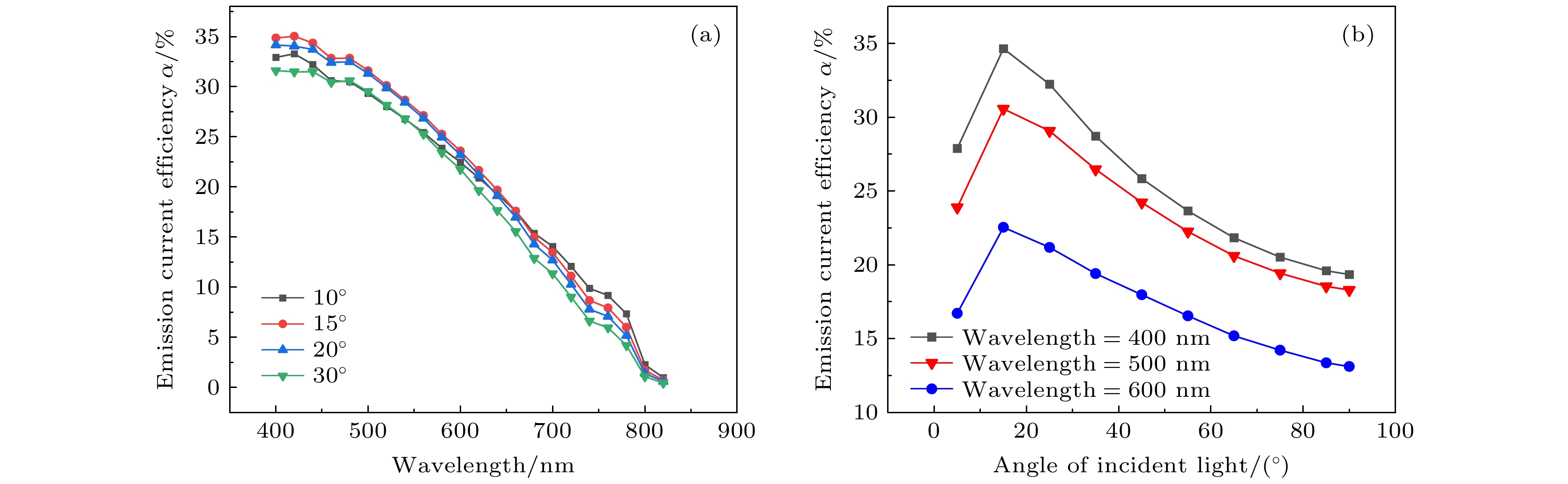
图 3 (a) 发射电流效率α随入射光波长变化曲线; (b) 发射电流效率α随入射光角度变化曲线, 其中阵列阴极Na, Nd, Tcp, Tp, Tn和Tcn分别为5×1018 cm–3, 1×1018 cm–3, 0.2 μm, 0.1 μm, 0.3 μm和1.0 μm
Fig. 3. (a) Emission current efficiency α versus incident wavelength; (b) emission current efficiency αversus incident light angle, where Na, Nd, Tcp, Tp, Tn and Tcn of the array cathode are 5×1018 cm–3, 1×1018 cm–3, 0.2 μm, 0.1 μm, 0.3 μm and 1.0 μm, respectively.
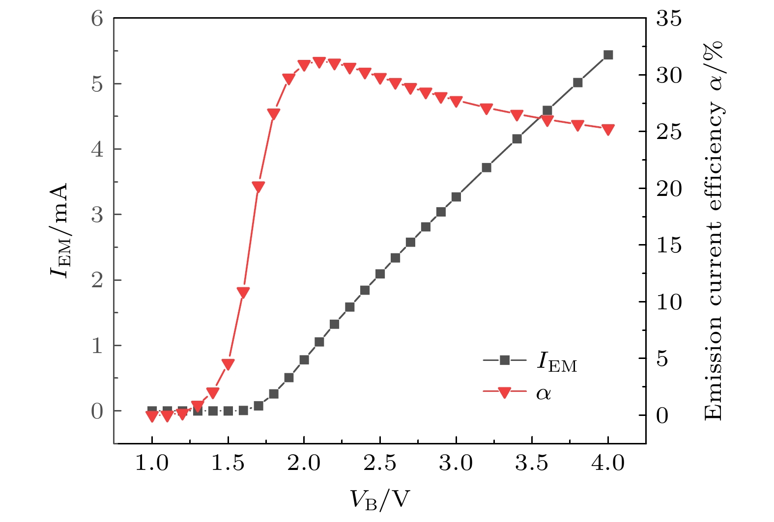
图 4 电注入阵列阴极发射电流和发射电流效率随电压变化曲线. 其中阵列阴极Na, Nd, Tcp, Tp, Tn和Tcn分别为5×1018 cm–3, 1×1018 cm–3, 0.1 μm, 0.1 μm, 0.3 μm和1.0 μm
Fig. 4. The cathodic emission current and emission current efficiency of the electrically implanted array vary with voltage. The array cathode Na, Nd, Tcp, Tp, Tn and Tcn are 5×1018 cm–3, 1×1018 cm–3, 0.1 μm, 0.1 μm, 0.3 μm, 1.0 μm, respectively.
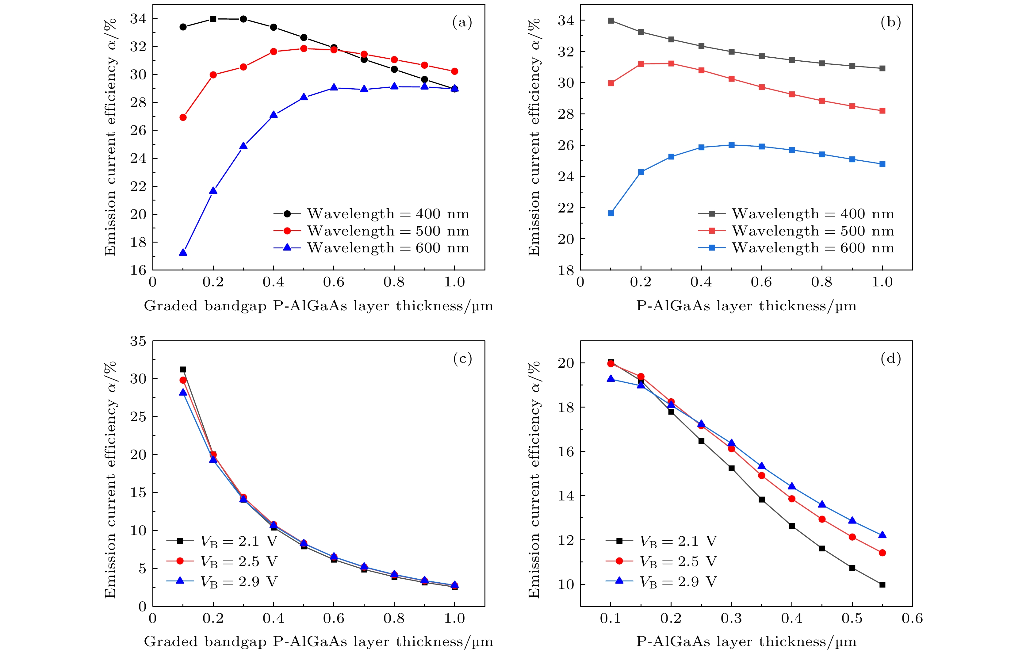
图 5 (a) 光注入时P型变带隙AlGaAs层厚度变化(a)和P型AlGaAs层厚度变化(b)对阵列阴极发射电流效率α的影响; 电注入时P型变带隙AlGaAs层厚度变化(c)和P型AlGaAs层厚度变化(d)对阵列阴极发射电流效率的影响. 其中光注入入射光角度为20°. (a)和(c)中Tp = 0.1 μm, (b)和(d)中Tcp = 0.2 μm, (a), (b), (c), (d)中阵列阴极Na, Nd, Tn和Tcn分别为5×1018 cm–3, 1×1018 cm–3, 0.3 μm和1.0 μm
Fig. 5. (a) The effect of the thickness change of P-band gap AlGaAs layer on the emission current efficiency of array cathode during optical injection; (b) the effect of thickness variation of P-type AlGaAs layer on emission current efficiency of array cathode during optical injection; (c) the effect of p-gap AlGaAs layer thickness variation on emission current efficiency of array cathode during electric injection; (d) the effect of thickness variation of P-type AlGaAs layer on emission current efficiency of array cathode during electric injection. The light injection angle is 20°. Tp is 0.1 μm in Figure (a) and Figure (c), Tcp is 0.2 μm in Figure (b) and Figure (d), and array cathode Na, Nd, Tn and Tcn are 5×1018 cm–3, 1×1018 cm–3, 0.3 μm and 1.0 μm in Figure (a), (b), (c) and (d), respectively.
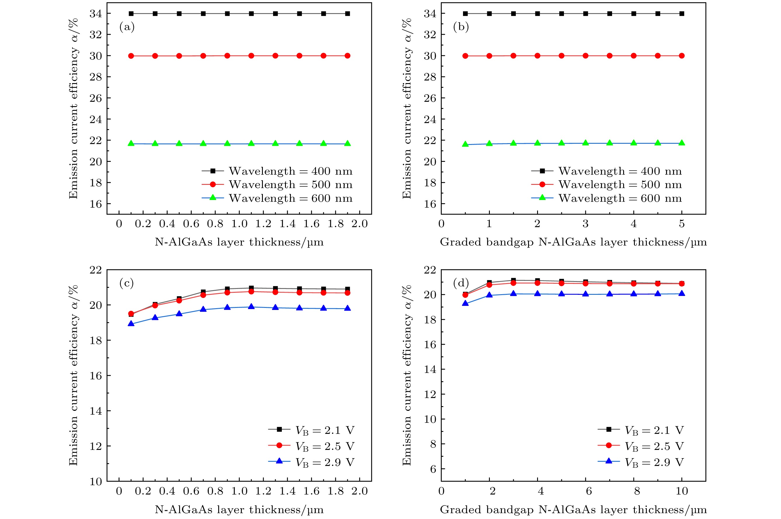
图 6 光注入时N型AlGaAs层厚度的变化对阵列阴极发射电流效率(a)和阵列阴极发射电流效率(b)的影响; 电注入时N型AlGaAs层厚度的变化对阵列阴极发射电流效率(c)和阵列阴极发射电流效率(d)的影响. 其中光注入入射光角度为20°, (a)和(c)中Tcn = 1 μm, (b)和(d)中Tcp = 0.3 μm, (a), (b), (c)和(d)中阵列阴极Na, Nd, Tcp和Tp分别为5×1018 cm–3, 1×1018 cm–3, 0.2 μm和0.1 μm
Fig. 6. (a) The effect of thickness variation of N-type AlGaAs layer on emission current efficiency of array cathode during optical injection; (b) effect of the thickness of N-type variable band gap AlGaAs layer on the emission current efficiency of array cathode during optical injection; (c) the effect of thickness variation of N-type AlGaAs layer on emission current efficiency of array cathode during electric injection; (d) the effect of the thickness of N-type variable band gap AlGaAs layer on the emission current efficiency of array cathode during electric injection. The light injection angle is 20°, Tcn is 1 μm in Figure (a) and Figure (c), Tcp is 0.3 μm in Figure (b) and Figure (d), and array cathode Na, Nd, Tcp and Tp are 5×1018 cm–3, 1×1018 cm–3, 0.2 μm and 0.1 μm in Figure (a), (b), (c) and (d), respectively.

图 7 (a) 光注入时P型AlGaAs层和P型变带隙AlGaAs层掺杂浓度Na变化对阵列阴极发射电流效率的影响; (b) 电注入时P型AlGaAs层和P型变带隙AlGaAs层掺杂浓度Na的变化对阵列阴极发射电流效率的影响. 其中光注入入射光角度为20º, 阵列阴极Nd, Tcp, Tp, Tn和Tcn分别为1 × 1018 cm–3, 0.2 μm, 0.1 μm, 0.3 μm和1.0 μm
Fig. 7. (a) The effect of doping concentration Na of P-type AlGaAs layer and P-type bandgap AlGaAs layer on emission current efficiency of array cathode during optical injection; (b) the effect of doping concentration Na of P-type AlGaAs layer and P-type bandgap AlGaAs layer on emission current efficiency of array cathode during electric injection. Incidence angle of optical injection is 20°, and the array cathode Nd, Tcp, Tp, Tn and Tcn are 1 × 1018 cm–3, 0.2 μm, 0.1 μm, 0.3 μm and 1.0 μm, respectively.
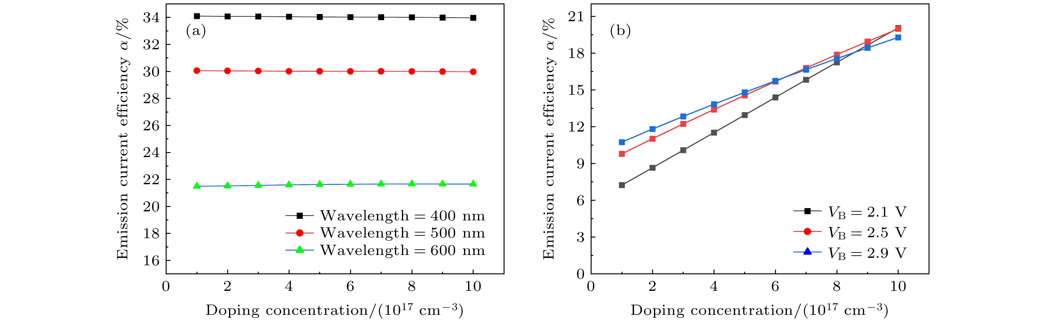
图 8 (a) 光注入时N型变带隙AlGaAs层和N-AlGaAs层掺杂浓度Nd变化对阵列阴极发射电流效率的影响; (b) 电注入时N型变带隙AlGaAs层和N-AlGaAs层掺杂浓度Nd的变化对阵列阴极发射电流效率的影响. 光注入入射光角度为20°, 阵列阴极Na, Tcp, Tp, Tn和Tcn分别为5 × 1018 cm–3, 0.2 μm, 0.1 μm, 0.3 μm和1.0 μm
Fig. 8. (a) Effect of doping concentration Nd variation of N-type bandgap AlGaAs layer and N-AlGaAs layer on emission current efficiency of array cathode during optical injection; (b) the effect of doping concentration Nd of N-type variable band gap AlGaAs layer and N-AlGaAs layer on emission current efficiency of array cathode during electric injection. Incidence angle of optical injection is 20°, and the array cathode Na, Tcp, Tp, Tn and Tcn are 5 × 1018 cm–3, 0.2 μm, 0.1 μm, 0.3 μm and 1.0 μm, respectively.
-
[1] Tsentalovich E, Barkhuff D, Chen J, Dodson G, Farkhondeh M, Franklin W, Ihloff E, Kaertner F, Tschalaer C, Yang B, Zwart T 2007 Nucl. Instrum. Methods Phys. Res., Sect. A 582 413
Google Scholar
[2] Benson S V, Douglas D, Neil G R, Shinn M D 2011 J. Phys. Conf. Ser. 299 012014
Google Scholar
[3] Liu W, Chen Y Q, Lu W T, Moy A, Poelker M, Stutzman M, Zhang S K 2016 Appl. Phys. Lett. 109 252104
Google Scholar
[4] Yamamoto N, Yamamoto M, Kuwahara M, Sakai R, Morino T, Tamagaki K, Mano A, Utsu A, Okumi S, Nakanishi T, Kuriki M, Bo C, Ujihara T, Takeda Y 2007 J. Appl. Phys. 102 024904
Google Scholar
[5] Pierce D T, Meier F 1976 Phys. Rev. B 13 5484
Google Scholar
[6] 滕利华, 牟丽君 2017 物理学报 66 046802
Google Scholar
Teng L H, Mu L J 2017 Acta Phys. Sin. 66 046802
Google Scholar
[7] Su C Y, Spicer W E, Lindau I 1983 J. Appl. Phys. 54 1413
Google Scholar
[8] Cultrera L, Galdi A, Bae J K, Ikponmwen F, Maxson J, Bazarov I 2020 Phys. Rev. Accel. Beams 23 023401
Google Scholar
[9] Machuca F, Liu Z, Sun Y, Pianetta P, Spicer W E, Pease R F W 2003 J. Vac. Sci. Technol. B 21 1863
Google Scholar
[10] Maruyama T, Brachmann A, Clendenin J E, Desikan T, Garwin E L, Kirby R E, Luh D A, Turner J, Prepost R 2002 Nucl. Instrum. Methods Phys. Res. Sect. A 492 199
Google Scholar
[11] 李晓峰 2001 博士学位论文 (西安: 中国科学院西安光学精密机械研究所)
Li X F 2001 Ph. D. Dissertation (Xi’an: Xi’an Institute of Optical and Precision Mechanics, Chinese Academy of Sciences) (in Chinese)
[12] Zhang Q, Bai X F, Cheng H C, Jiao G C, Li Z K, Han K, Li Q 2022 Acta Photonica Sin. 51 0304005
Google Scholar
[13] Liu L, Lu F F, Tian J, Zhangyang X Y, Lv Z S 2020 J. Mater. Sci. Technol. 58 86
Google Scholar
[14] 邓文娟, 彭新村, 邹继军, 江少涛, 郭栋, 张益军, 常本康 2014 物理学报 63 167902
Google Scholar
Deng W J, Peng X C, Zou J J, Jiang S T, Guo D, Zhang Y J, Chang B K 2014 Acta Phys. Sin. 63 167902
Google Scholar
[15] 邹继军, 高频, 杨智, 常本康 2008 光子学报 37 1112
Zou J J, Gao P, Yang Z, Chang B K 2008 Acta Photonica Sin. 37 1112
[16] Xia S, Liu L, Kong Y K 2016 Opt. Quantum Electron. 48 306
Google Scholar
[17] 张涛 2018 电子世界 15 65
Zhang T 2018 Electron. World 15 65
[18] 曾梦丝, 彭新村 2018 光学仪器 40 67
Zeng M S, Peng X C 2018 Opt. Instrum. 40 67
[19] 邹继军, 张益军, 杨智, 常本康 2011 物理学报 60 017902
Google Scholar
Zou J J, Zhang Y J, Yang Z, Chang B K 2011 Acta Phys. Sin. 60 017902
Google Scholar
[20] Xia J Y, Zou J J, Peng X C, Deng W J, Zhang Y J 2020 Ultramicroscopy 219 113121
Google Scholar
[21] Ding X J, Ge X W, Zou J J, Zhang Y J, Peng X C, Deng W J, Chen Z P, Zhao W J, Chang B K 2016 Opt. Commun. 367 149
Google Scholar

 下载:
下载:
计量
- 文章访问数: 5981
- PDF下载量: 62
- 被引次数: 0
