Search

Article

x
Special topic

更多 
Topics
Article Type

SPECIAL TOPIC—Toward making functional devices at an atomic scale: Fundamentals and frontiers

“原子制造:基础研究与前沿探索”专题编者按 

特邀编辑: 高鸿钧 中国科学院物理研究所   

DOI: 10.7498/aps.70.020101 

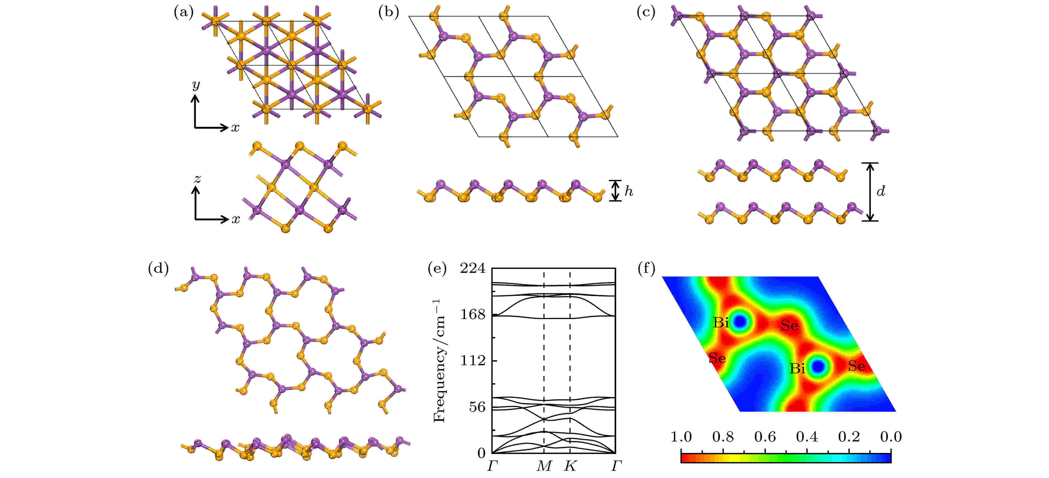
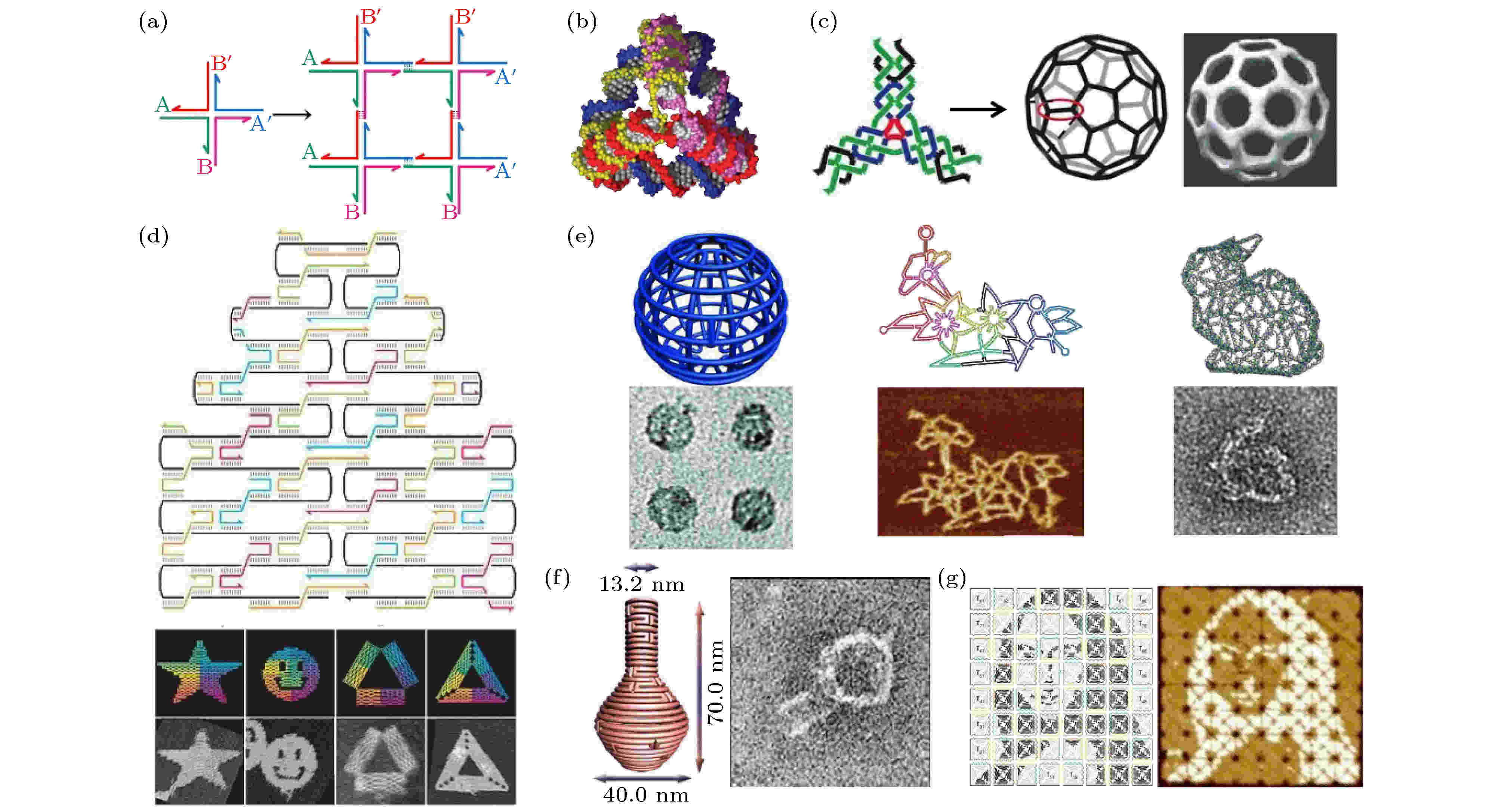
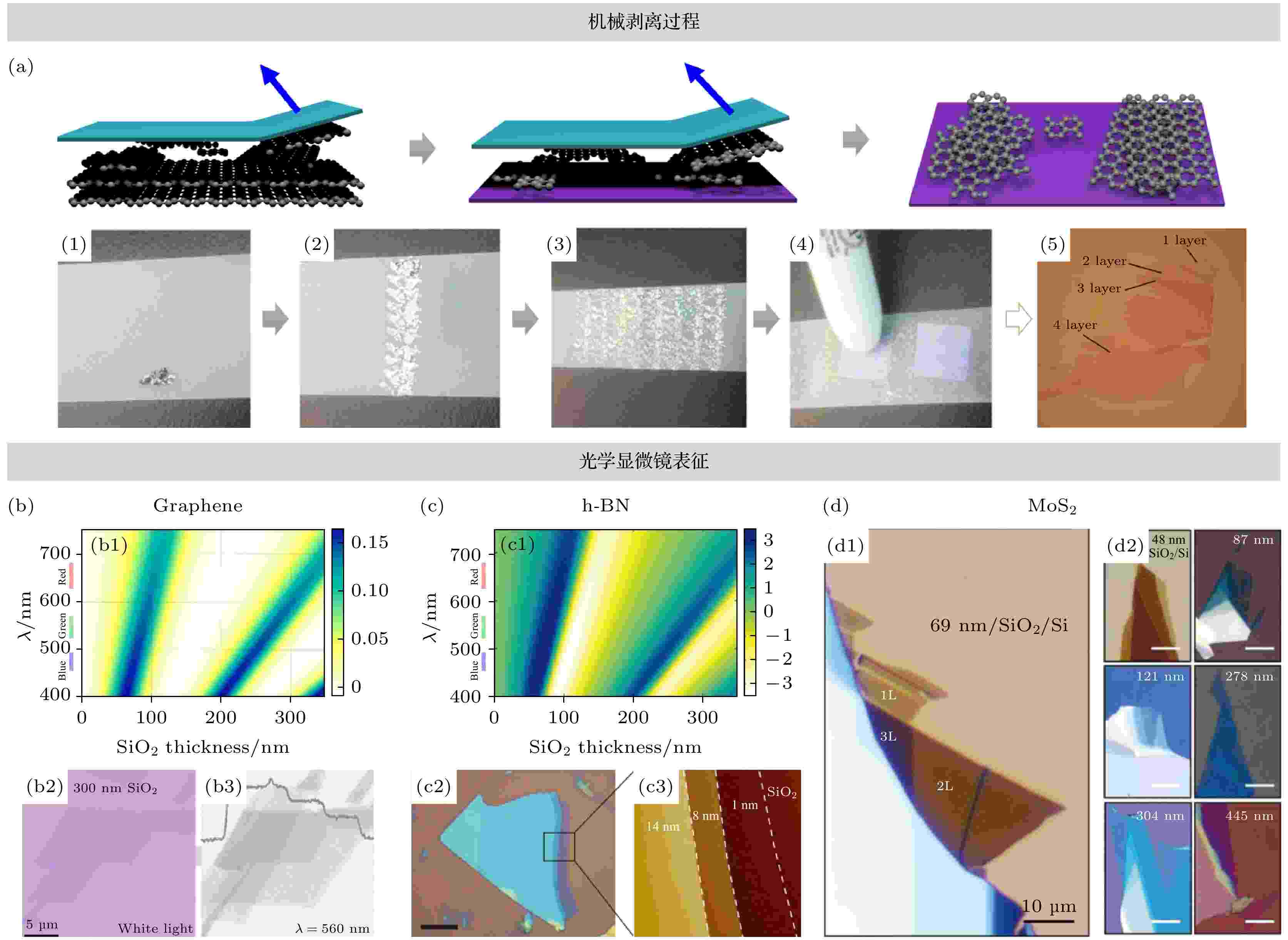
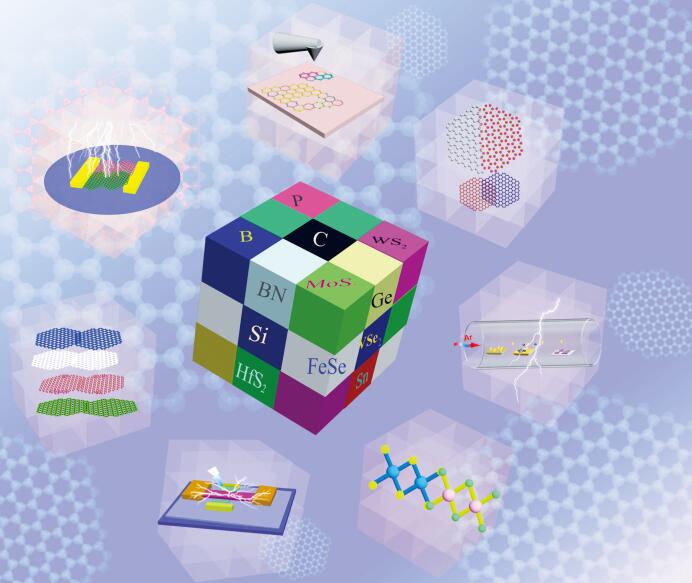
          制造技术的不断迭代发展带来了器件性能的飞跃, 也推动着人类技术的进步. 伴随着器件特征尺寸的不断缩小, 制造技术先后经历了宏观制造、介观制造、微观制造和纳米制造等多个阶段, 当前最具代表性的半导体工艺, 已经从微米尺度走到最前沿的3 nm 左右, 并进一步向更小的尺度迈进.因此, 制造技术进入到原子尺度已不再是遥不可及的梦想, 而成为现在科技界研究前沿的现实对象.然而, 在原子尺度下, 常规制造技术在材料、结构和器件的制造过程中遇到了原理性和系统性的瓶颈和壁垒, 这种制造精度的提升将不再是线性微缩, 而是从经典行为到量子行为的跨越, 势必孕育出颠覆性的新材料、新器件和新原理. 例如, 有限原子数的小团簇会呈现与块体截然不同的结构和物理性质, 甚至产生类似高温超导的“能隙”; 超导基底上的铁磁原子线会形成马约拉纳费米子器件,是拓扑量子计算的载体; 二维原子晶体材料家族中, 石墨烯的费米速度比块材石墨高上千倍, 扭角石墨烯则可以形成奇特的莫特绝缘体态, 单层的二硫化钼具有比块材高10 万倍的二阶非线性光学系数; 原子精确操控的晶体管有可能形成相干的高质量量子点阵列, 也有可能成为具有选择性的极限单分子灵敏度的气体传感器, 等等. 因此, 单原子层次上的功能器件设计与制造—原子制造, 迅速成为当前科学、技术和产业界共同关注的前沿研究热点. 原子制造是采用“自下而上”的变革性技术路线, 在原子水平的高效制造工艺, 是精细制造技术发展的必然趋势, 也是物质科学的终极梦想之一. 我们希望从原子这一常规物质世界的底层, 通过对单原子的精细操控, 制备新型原子材料, 构筑新器件, 并制作出新系统, 为解决“未来制造”提供一条从基础研究出发的新路线. 

       正是在这种科学梦想的感召及各级部门的关心和鼎力支持下, 国内快速形成了一支有影响力的学术队伍, 出现了一批优秀的工作, 使得我们出版一个以原子制造为主题的专辑成为可能. 同时, 为了帮助读者系统了解原子制造—单原子层次上功能器件制造—的前沿研究与最新进展, 推动原子制造技术及相关研究的进一步发展, 本刊特邀请部分活跃在本领域前沿各研究方向的专家, 围绕原子制造主题, 从材料、物理、化学、力学、模拟、实验和理论等诸方面, 以不同的视角介绍最新进展、问题、现状和展望. 专题内容包括: 1) 原子尺度的制造与检测工艺; 2) 二维原子材料与器件的研究; 3) 其他原子水平的材料与器件研究.我相信并希望“原子制造: 基础研究与前沿探索”专辑能对相关研究提供有价值的参考, 推动该领域的发展, 为国家科技发展做出重要贡献.

客座编辑:杜世萱 中国科学院物理研究所; 宋凤麒 南京大学; 戴庆 国家纳米科学中心
Acta Physica Sinica. 2021, 70(2).
Electronic structures, chemical bonds, and stabilities of ${\rm{Ta}}_4{\rm{C}}_n^{-/0} $ (n = 0–4) clusters: Anion photoelectron spectroscopy and theoretical calculations
Zhang Chao-Jiang, Xu Hong-Guang, Xu Xi-Ling, Zheng Wei-Jun
2021, 70 (2): 023601. doi: 10.7498/aps.70.20201351
Abstract +
The electronic structures, chemical bonds and stabilities of ${\rm{Ta}}_4{\rm{C}}_n^{-/0} $ (n = 0–4) clusters are investigated by combining anion photoelectron spectroscopy with theoretical calculations. The vertical detachment energy values of ${\rm{Ta}}_4{\rm{C}}_n^{-} $ (n = 0–4) anions are measured to be (1.16 ± 0.08), (1.35 ± 0.08), (1.51 ± 0.08), (1.30 ± 0.08), and (1.86 ± 0.08) eV, and the electron affinities of neutral Ta4Cn (n = 0–4) are estimated to be (1.10 ± 0.08), (1.31 ± 0.08), (1.44 ± 0.08), (1.21 ± 0.08), and (1.80 ± 0.08) eV, respectively. It is found that the geometry structure of ${\rm{Ta}}_4^- $cluster is a tetrahedron, and the most stable structure of ${\rm{Ta}}_4{\rm{C}}_1^{-} $ has a carbon atom capping one face of the ${\rm{Ta}}_4^- $ tetrahedron, while in the ground state structure of ${\rm{Ta}}_4{\rm{C}}_2^{-} $ cluster, two carbon atoms cap two faces of the${\rm{Ta}}_4^- $ tetrahedron, respectively. The lowest-lying isomer of ${\rm{Ta}}_4{\rm{C}}_3^{-} $ cluster holds a cube-cutting-angle structure. The ground state structure of ${\rm{Ta}}_4{\rm{C}}_4^{-} $ is a 2 × 2 × 2 cube. The neutral Ta4Cn (n = 0–4) clusters have similar structures to their anionic counterparts and the neutral Ta4C4 cluster can be considered as the smallest cell for α-TaC face-centered cube crystal. The analyses of molecular orbitals reveal that the SOMO of ${\rm{Ta}}_4{\rm{C}}_3^{-} $ is mainly localized on one tantalum atom, inducing a low VDE. Our results show that the Ta-Ta metal bonds are replaced by Ta-C covalent bonds gradually as the number of carbon atoms increases in ${\rm{Ta}}_4{\rm{C}}_n^{-/0} $ (n = 0–4) clusters. The per-atom binding energy values of ${\rm{Ta}}_4{\rm{C}}_n^{-/0} $ (n = 0–4) clusters are higher than those of ${\rm{Ta}}_{4+n}^{-/0} $ (n = 0–4) clusters, indicating that the formation of Ta-C covalent bonds may raise the melting point. The per-atom binding energy of neutral Ta4C4 is about 7.13 eV, which is quite high, which may contribute to the high melting point of α-TaC as an ultra-high temperature ceramic material.
Investigation of artificial quantum structures constructed by atom manipulation
Li Yu-Ang, Wu Di, Wang Dong-Li, Hu Hao, Pan Yi
2021, 70 (2): 020701. doi: 10.7498/aps.70.20201501
Abstract +
The atom manipulation technique based on scanning tunneling microscope refers to a method of relocating single atoms or molecules on a certain surface at atomic accuracy by using an atomically sharp tip, which is a unique and powerful tool for studying the quantum physics and prototype quantum devices on a nanometer scale. This technique allows us to build artificial structure atom-by-atom, thus some desired interesting quantum structures which are difficult to grow or fabricate by conventional methods could be realized, and unique quantum states, spin order, band structure could be created by the fine tuning of the structural parameters like lattice constant, symmetry, periodicity, etc. Combined with nanosecond scale time domain electric measurement and autonomous control technique, the atom manipulation would be useful in exploring the atomic precision prototype quantum devices, and providing some valuable knowledge for future electronics. In this review, we introduce the atom manipulation technique and related milestone research achievements and latest progress of artificial quantum structures, including electronic lattices with exotic quantum states on Cu(111), quantum dots on III-V semiconductors, magnetic structures with tunable spin order, structures for quantum information storage and processing, prototype Boolean logic devices and single atom devices. The STM lithography and autonomous atom manipulation are discussed as well. With such improvements, this technique would play more important roles in developing the functional quantum devices in future.
Nucleic acid-metal complex and its application in atomic-scale manufacturing
Li Sheng-Kai, Hao Qing, Peng Tian-Huan, Chen Zhuo, Tan Wei-Hong
2021, 70 (2): 028102. doi: 10.7498/aps.70.20201430
Abstract +
Atomic-scale and close-to-atomic scale manufacturing, a frontier hot issue in international academic research, is a cutting-edge manufacturing technique in which atoms are directly used as the manipulation object and atomic-scale structures with specific functions are established to meet the requirements for mass productions. This review focuses on precise atomic-scale manufacturing technology of nucleic acid materials. Firstly, the basic structures and functions of nucleic acid materials are introduced, and the basic principles of the interaction between DNA and metal atoms are discussed. Then the development process and breakthrough progress of nucleic acid materials-mediated precise atomic-scale manufacturing are introduced from the aspects of natural nucleic acid materials, artificial base “molecular elements”, and nucleic acid nanostructures. Finally, the challenges and opportunities in this field are systematically summarized and some suggestions for future development are given.
First-principle study of new phase of layered Bi2Se3
Guo Yu, Zhou Si, Zhao Ji-Jun
2021, 70 (2): 027102. doi: 10.7498/aps.70.20201434
Abstract +
Recently, the boom of graphene has aroused great interest in searching for other two-dimensional (2D) compound materials, which possess many intriguing physical and chemical properties. Interestingly, 2D allotropes of differing atomic structures show even more diverse properties. The Bi2Se3 has attracted much attention due to its unique physical properties, while its allotrope has not been investigated. Based on first-principle calculations, here in this work we predict a new phase of Bi2Se3 monolayer with outstanding dynamic and thermal stabilities, named as β-Bi2Se3. Notably, the β-Bi2Se3 monolayer is a semiconductor with a modest direct band gap of 2.40 eV and small effective mass down to 0.52m0, large absorption coefficient of 105 cm–1 in the visible-light spectrum, suitable band edge positions for photocatalysis of water splitting. Moreover, the breaking of mirror symmetry in β-Bi2Se3 along the out-of-plane direction induces vertical dipolar polarization, yielding a remarkable out-of-plane piezoelectric coefficient of 0.58 pm/V. These exceptional physical properties render the layered Bi2Se3 a promising candidate for future high-speed electronics and optoelectronics.
Recent progress of frame nucleic acids studies towards atomic fabrications
Yang Bei, Li Qian, Liu Hua-Jie, Fan Chun-Hai
2021, 70 (2): 026201. doi: 10.7498/aps.70.20201437
Abstract +
In recent years, the technology of traditional integrated circuit fabrication is facing a huge challenge. As the top-down lithography gradually approaches to its size limit, the development of atomic-scale precise fabrication for functional devices has already become a major scientific issue at present and might become a breakthrough in the development of information technology in the future. With the reference of the bottom-up self-assembly, which is the basic principle of constructing various advanced structures in living systems, the integrated assembly of atoms can be gradually constructed through a series of operations such as capturing, positioning, and moving atoms. The advent of framework nucleic acids (FNAs) happens to provide a new platform for manipulating single atom or integrating multiple atoms. As is well known, the nucleic acids are not only the carriers of genetic information, but also biological building blocks for constructing novel microscopic and macroscopic materials. The FNAs represent a new type of framework with special properties and features, constructed by nucleic acids’ bottom-up self-assembly. With the improvement of chemical synthesis and modification method of nucleic acids, various molecules and materials, such as fluorophores, nanoparticles, proteins, and lipids, can be spatially organized on FNAs with atomic precision, and these functionalized FNAs have been widely explored in the fields of biosensing, biocomputing, nano-imaging, information storage, nanodevices, etc. Based on the features of precise addressability, superior programmability and tailorable functionality, FNAs can be used for implementing the artificial self-assembly of objects with atomic precision to realize the precise arrangement in spatial and functional integration of basic assembly units, and even prompt the development of device fabrication from atomic scale to macroscopic scale. This review focuses on the intersection of FNAs and atomic fabrication, giving a systematically description of the feasibility and advantages of precisely atomic fabrication with FNAs from three aspects. First, the DNA/RNA nanoarchitectures from static state to dynamic state and general strategies for programmable functionalization of FNAs are briefly introduced. Then the applications of FNAs in device fabrication are highlighted, including single molecule reactors, single molecule sensors, nanodevices for cargo loading and transporting, nanophotonics, nanoelectronics and information processing devices. Finally, an outlook of the future development of atomic fabrication with FNAs is given as well.
Evolution from dip-pen nanolithography to mechanochemical printing
Yu Yi-Fei, Cao Yi
2021, 70 (2): 024202. doi: 10.7498/aps.70.20201537
Abstract +
As a unique nanomanipulation and nanofabrication tool, dip-pen nanolithography (DPN) has enjoyed great success in the past two decades. The DPN can be used to create molecular patterns with nanoscale precision on a variety of substrates with different chemistry properties. Since its advent, the DPN has been steadily improved in the sense of applicable inks, fabrication throughput, and new printing chemistry. Among these developments, mechanical force induced mechanochemistry is of special interest.In this review, we introduce the physical principles behind the DPN technique. We highlight the development of DPN for writing with various types of “inks”, including small molecules, viscous polymer solutions, lipids, and biomolecules, especially, the development of thermal-DPN allowing printing with inks that are usually in solid phase at room temperature. Next, we introduce the parallel-DPN and polymer pen nanolithography. These techniques greatly speed up the fabrication speed without sacrificing the precision. We also summarize the advances in chemical reaction based DPN technologies, including electrochemical DPN, metal tip-induced catalytical DPN, and mechanochemical DPN (or mechanochemical printing). To further elaborate the mechanism behind the mechanochemical printing, we briefly review the development of mechanochemistry, including the reaction mechanism, various experimental approaches to realizing mechanochemistry, and recent development in this field. We highlight the advantages of using atomic force microscopy to study mechanochemistry at a single molecule level and indicate the potential of combining this technique with DPN to realize mechanochemical printing. We envision that with the further discovery of novel mechanophores that are suitable for mechanochemical printing, this technique can be broadly applied to nanotechnology and atomic fabrication.
Controllable preparation and photoelectric applications of two-dimensional in-plane and van der Waals heterostructures
Yao Wen-Qian, Sun Jian-Zhe, Chen Jian-Yi, Guo Yun-Long, Wu Bin, Liu Yun-Qi
2021, 70 (2): 027901. doi: 10.7498/aps.70.20201419
Abstract +
Since the discovery of graphene, two-dimensional (2D) materials have received continuous attention and carried out in-depth exploration and development due to their excellent properties. With the exploration of the preparation of new 2D materials, one began to consider the synergistic effects produced by the in-plane junction and interlayer stacking to compensate for the defects of a single material and obtain some new properties. Matching the lattice structure to achieve specific functionalization, or using van der Waals force to achieve stacking, helps to introduce a new degree of freedom by combining different 2D materials, and open a new window for the research and practical application of 2D materials.From the perspective of atomic manufacturing, in this article we introduce the controllable preparation and optoelectronic applications of 2D planar and van der Waals heterojunction materials. First, we briefly introduce the common 2D materials such as graphene, hexagonal boron nitride, transition metal dichalcogenides and black phosphorus used in the preparation of heterojunctions and related concepts of heterojunctions. Second, we review, in principle, the commonly used characterization methods including scanning probe-based techniques, spectrum-based, electron-based imaging techniques and others. Third, we summarize the preparation methods of planar and vertical heterojunctions. Basically, mechanical transfer method such as wet or dry method can be used to produce various vertical heterostructures of 2D materials, but usually lack the scalability. On the other hand, chemical vapor deposition method provides a scalable route to producing the planar heterostructure and vertical structure of 2D materials. Several strategies have been developed to produce various heterostructures. In addition, the recent development of twist-angle and quasi-crystalline bi-layer graphene is briefly reviewed. Fourth, the properties and applications of 2D van der Waals heterostructures such as field-effect transistor, light emitting diode, solar cell, flexible optoelectronic devices and plasmonic applications are introduced. Finally, the problems in the field are discussed, and the outlook is provided.
Optical properties of two-dimensional black phosphorus
Huang Shen-Yang, Zhang Guo-Wei, Wang Fan-Jie, Lei Yu-Chen, Yan Hu-Gen
2021, 70 (2): 027802. doi: 10.7498/aps.70.20201497
Abstract +
Recently, black phosphorus (BP), an emerging layered two-dimensional (2D) material, has aroused much research interest. Distinguished from most of other 2D materials, BP is always a direct bandgap semiconductor regardless of the thickness, with the bandgap ranging from 0.3 eV (bulk) to 1.7 eV (monolayer), which is just fill the gap in the bandgap between graphene and transition metal dichalcogenides (TMDCs) in this frequency range. Besides, the BP exhibits many intriguing properties, such as high carrier mobility, highly tunable and anisotropic physical properties, which render the BP another star 2D material following graphene and TMDCs. In this review, we mainly focus on the advances in the optical properties of 2D BP, with the content covering the intrinsic optical properties and external perturbation effects on optical properties. Regarding the intrinsic optical properties, we introduce the anisotropic and layer-dependent optical absorption from interband transitions, the layer-dependent exciton binding energy and exciton absorption, visible-to-infrared photoluminescence, and stability of absorption and photoluminescence. As for external perturbation effects on optical properties, we introduce in-plane uniaxial and biaxial strain effects, gate-induced quantum confined Franz-Keldysh effect and Burstein-Moss effect. And finally we give a brief summary and outlook, pointing out some several interesting and important issues of BP, which need further studying urgently such as hyperbolic plasmons, intersubband transitions, optical properties in heterostructures and twist angle moiré superlattice and so on. This review gives an overview of the optical properties of BP and is expected to arouse the interest in further studying the BP.
Fundamental principles, key enabling technologies, and research progress of atom chips
Li Mo, Chen Fei-Liang, Luo Xiao-Jia, Yang Li-Jun, Zhang Jian
2021, 70 (2): 023701. doi: 10.7498/aps.70.20201561
Abstract +
The laser cooling, trapping and manipulating of neutral atoms has become a valuable tool for scientists, providing innovative ways to probe the nature of reality and giving rise to transformative devices in the fields of precise measurement and quantum information processing. Unlike traditional complex and bulky atomic experimental facilities, atom chips, through the design, fabrication of surface-patterned microstructures, and the integration of devices on the substrates, can precisely control the magnetic, electric or optical fields on a micro-nano scale with low power consumption. It can realize strong trapping as well as coherent atomic manipulation. Since atom chip was first proposed twenty years ago, it has built a robust quantum platform for miniaturizing and integrating quantum optics and atomic physics tools on a chip. In this paper, first, we briefly review the development history of atom chips, then introduce the basic knowledge of micro potential traps and micro guides based on on-chip current-carrying wires. Afterwards, the key technologies about the chip material, design, fabrication, characterization and integration of atom chips are discussed in detail. We not only focus on the currently most active and successful areas - current carrying wires, but also look at more visionary approaches such as to the manipulation of atoms with real nano structures, say, carbon nano tubes. The design and fabrication principles of ideal atom chips are discussed as well. In the forth part, the worldwide plans and research projects involving with atom chip technologies are summarized, showing that many countries see this as an important foundational technology. Following that, the major developments in the application fields including atom clocks, atom interferometer gyroscope, cold atom gravimeter, etc are described. Finally, the challenges faced by atom chips towards practical application are pointed out and the prospects for their subsequent development are depicted.
Methods of transferring two-dimensional materials
Liao Jun-Yi, Wu Juan-Xia, Dang Chun-He, Xie Li-Ming
2021, 70 (2): 028201. doi: 10.7498/aps.70.20201425
Abstract +
The advent of two-dimensional (2D) materials, a family of materials with atomic thickness and van der Waals (vdWs) interlayer interactions, offers a new opportunity for developing electronics and optoelectronics. For example, semiconducting 2D materials are promising candidates for extending the Moore's Law. Typical 2D materials, such as graphene, hexagonal boron nitride (h-BN), black phosphorus (BP), transition metal dichalcogenides (TMDs), and their heterostrcutures present unique properties, arousing worldwide interest. In this review the current progress of the state-of-the-art transfer methods for 2D materials and their heterostructures is summarized. The reported dry and wet transfer methods, with hydrophilic or hydrophobic polymer film assistance, are commonly used for physical stacking to prepare atomically sharp vdWs heterostructure with clear interfaces. Compared with the bottom-up synthesis of 2D heterostructures using molecular beam epitaxy (MBE) or chemical vapor deposition (CVD), the construction of 2D heterostructures by transfer methods can be implemented into a curved or uneven substrate which is suitable for pressure sensing, piezoelectric conversion as well as other physical properties’ research. Moreover, the transfer of 2D materials with inert gas protected or in vacuum operation can protect moisture-sensitive and oxygen-sensitive 2D materials from degerating and also yield interfaces with no impurities. The efficient and non-destructive large-area transfer technology provides a powerful technical guarantee for constructing the 2D heterostructures and exploring the intrinsic physical and chemical characteristics of materials. Further development of transfer technology can greatly facilitate the applications of 2D materials in high-temperature superconductors, topological insulators, low-energy devices, spin-valley polarization, twistronics, memristors, and other fields.
Valleytronic properties and devices based on two-dimensional atomic layer materials
Sun Zhen-Hao, Guan Hong-Ming, Fu Lei, Shen Bo, Tang Ning
2021, 70 (2): 027302. doi: 10.7498/aps.70.20201415
Abstract +
Artificial manipulation of electronic degrees of freedom is the key point to realize modern electronic devices. Both charge and spin of electron have been widely studied and applied to logic circuits and information storage devices. Valley, the unique degree of freedom of crystal electrons, has also attracted great attention of the researchers in the past decade. The valleytronics progress benefits from the tremendous improvements of the two-dimensional atomic layer material growth technologies and in-depth explorations of valley properties. Valleytronic materials, represented by two-dimensional transition metal dichalcogenides, have become an excellent platform for the research and design of new electronic devices due to their special optical responses and distinctive electronic transport properties. The valley devices have the advantages of fast operation, low energy consumption, less information loss, high integration and long transmission distance.In this review, we first introduce the basic concepts and properties of the energy valley, such as the valley Hall effect and the valley circular dichroism. Second, we describe the crystal structures and energy band diagrams of the two-dimensional transition metal dichalcogenides. Third, the progress in artificial manipulation of the valley effects is summarized. Some approaches which can break the inversion symmetry and therefore induce the valley degree of freedom are introduced. Fourth, we discuss the methods of realizing valley polarization. Fifth, the developments of valleytronic devices in recent years are reviewed. Finally, a summary and an outlook are given.
Development and application of vapor deposition technology in atomic manufacturing
Guo Qin-Min, Qin Zhi-Hui
2021, 70 (2): 028101. doi: 10.7498/aps.70.20201436
Abstract +
With the development of future information devices towards smaller size, lower power consumption and higher performance, the size of materials used to build devices will be further reduced. Traditional “top-down” technology has encountered a bottleneck in the development of information devices on a nanoscale, while the vapor deposition technology has attracted great attention due to its ability to construct nanostructures on an atomic scale, and is considered to have the most potential to break through the existing manufacturing limits and build nano-structures directly with atoms as a “bottom-up” method. During molecular beam epitaxy, atoms and molecules of materials are deposited on the surface in an “atomic spray painting” way. By such a method, some graphene-like two-dimensional materials (e.g., silicene, germanene, stanene, borophene) have been fabricated with high quality and show many novel electronic properties, and the ultrathin films (several atomic layers) of other materials have been grown to achieve certain purposes, such as NaCl ultrathin layers for decoupling the interaction of metal substrate with the adsorbate. In an atomic layer deposition process, which can be regarded as a special modification of chemical vapor deposition, the film growth takes place in a cyclic manner. The self- limited chemical reactions are employed to insure that only one monolayer of precursor (A) molecules is adsorbed on the surface, and the subsequent self- limited reaction with the other precursor (B) allows only one monolayer of AB materials to be built. And the self- assembled monolayers composed of usually long- chain molecules can be introduced as the active or inactive layer for area- selective atomic layer deposition growth, which is very useful in fabricating nano- patterned structures. As the reverse process of atomic layer deposition, atomic-layer etching processes can remove certain materials in atomic precision. In this paper we briefly introduce the principles of the related technologies and their applications in the field of nano- electronic device processing and manufacturing, and find how to realize the precise control of the thickness and microstructure of functional materials on an atomic scale.
Chemical vapor deposition growth of large-areas two dimensional materials: Approaches and mechanisms
Wang Shuo, Wang Wen-Hui, Lü Jun-Peng, Ni Zhen-Hua
2021, 70 (2): 026802. doi: 10.7498/aps.70.20201398
Abstract +
Two-dimensional (2D) layered materials have attracted increasing attention in recent years because of their abundant material categories and superior physical/chemical properties. In order to satisfy the requirements for highly integrated devices in the post-Moore era, substantial efforts have been devoted to producing atomically thin 2D materials with large lateral dimensions and high crystalline quality. The controllable synthesis is the precondition of the implementation of large mass producing 2D material in industry. Chemical vapor deposition (CVD) is a powerful method widely used in the synthesis of 2D materials and their hybrid structures. However, it is still challengeable to flexibly and easily grow any 2D materials into large area. Therefore, a systematic understanding of the requirements for controllable growth of different 2D materials are desired. In this review article, we provide a comprehensive discussion on the influencing factors, material transport, nucleation and growth rate in the CVD growth process. Finally, the strategies to further improve the size and quality of 2D materials are prospected.
Electronic properties of two-dimensional Janus atomic crystal
Wang Pan, Zong Yi-Xin, Wen Hong-Yu, Xia Jian-Bai, Wei Zhong-Ming
2021, 70 (2): 026801. doi: 10.7498/aps.70.20201406
Abstract +
Since the advent of graphene, two-dimensional materials with various novel properties have received more and more attention in the fields of optoelectronic devices, spintronics and valley electronic devices. Among them, the excellent properties that appear in graphene with various molecular groups for asymmetric functionalization have led to the research of other Janus two-dimensional materials with asymmetric surface characteristics. As an important derivative of two-dimensional materials, Janus two-dimensional materials (especially Janus transition metal chalcogenides) have become a research hotspot in recent years. Both experiment and theory have confirmed that this kind of material has mirror asymmetry and novel characteristics, such as strong Rashba effect and out-of-plane piezoelectric polarization, and thus showing a great prospect for its applications in sensors, actuators, and other electromechanical devices. In this review we introduce the recent research progress of emerging Janus two-dimensional materials (including Janus graphene, various Janus two-dimensional materials and Janus two-dimensional van der Waals heterojunction), and summarize the unique electronic properties and potential applications of Janus two-dimensional materials. Finally, we draw some conclusions and depict a prospect of further exploration of Janus two-dimensional materials.
First principles calculation of two-dimensional materials at an atomic scale
Liu Zi-Yuan, Pan Jin-Bo, Zhang Yu-Yang, Du Shi-Xuan
2021, 70 (2): 027301. doi: 10.7498/aps.70.20201636
Abstract +
With the continuous development of information and technology, core components are developing rapidly toward faster running speed, lower energy consumption, and smaller size. Due to the quantum confinement effect, the continuous reduction of size makes materials and devices exhibit many exotic properties that are different from the properties of traditional three-dimensional materials. At an atomic scale level, structure and physical properties, accurately synthesizing, characterizing of materials, property regulation, and manufacturing of electronic devices with good performance all play important roles in developing the electronic devices and relevant applications in the future. Theoretical calculation can efficiently predict the geometric structure, physical properties and interface effects with low consumption but high accuracy. It is an indispensable research means of atomic level manufacturing technology. In this paper, we review the recent progress of two-dimensional materials from the theoretical perspective. This review is divided into three parts, i.e. two-dimensional layered materials, two-dimensional non-layered materials, and two-dimensional heterostructures. Finally, we draw some conclusions and suggest some areas for future investigation.
Terahertz measurement based on Rydberg atomic antenna
Chen Zhi-Wen, She Zhen-Yue, Liao Kai-Yu, Huang Wei, Yan Hui, Zhu Shi-Liang
2021, 70 (6): 060702. doi: 10.7498/aps.70.20201870
Abstract +
Rydberg atoms have large electric dipole moments in the microwave and terahertz frequency band. The detection of electromagnetic field intensity in this frequency band can be achieved by using quantum interference effects. Theoretically, this detection method can have a sensitivity much higher than the traditional detection methods. Therefore, electromagnetic field detection and precision measurement technology based on Rydberg atomic quantum effects has great application prospects in terahertz field strength and power measurement, terahertz communication and imaging. In this paper, we review the basic theory and experimental methods to realize the self-calibration and traceability measurement of electromagnetic field based on Rydberg atomic quantum effects. The principle and technical scheme of high-sensitivity terahertz field strength measurement, terahertz near-field high-speed imaging and terahertz digital communication based on Rydberg atom are introduced in detail. Finally, the processing terahertz detection work based on Rydberg atom by our research team is also mentioned briefly.
High-sensitive microwave sensor and communication based on Rydberg atoms
Fan Jia-Bei, Hao Li-Ping, Bai Jing-Xu, Jiao Yue-Chun, Zhao Jian-Ming, Jia Suo-Tang
2021, 70 (6): 063201. doi: 10.7498/aps.70.20201401
Abstract +
We present a high-sensitivity weak microwave measurement and communication technology by employing the Rydberg beat technique. The Rydberg cascade three-level system is composed of a cesium ground state $6{\rm{S}}_{1/2}$, an excited state $6{\rm{P}}_{3/2}$, and a Rydberg state $n{\rm{D}}_{5/2}$ in a room-temperature cesium cell. A two-photon resonant Rydberg electromagnetic induced transparency (EIT) is used to optically detect the Rydberg level, in which a weak probe laser is locked at the resonant transition of $|6{\rm{S}}_{1/2}\rangle \rightarrow |6{\rm{P}}_{3/2}\rangle$, and a strong coupling laser drives the transition of $|6{\rm{P}}_{3/2}\rangle \rightarrow |n{\rm{D}}_{5/2}\rangle$. Both lasers are locked with a high-precision Fabry-Perot cavity. Two E-fields are incident into the vapor cell to interact with Rydberg atoms via a microwave horn, one is a strong microwave field with frequency 2.19 GHz, acting as a local field ($E_{{\rm{L}}}$) and resonantly coupling with two Rydberg energy levels, $|68{\rm{D}}_{5/2}\rangle$ and $|69{\rm{P}}_{3/2}\rangle$, and the other is a weak signal field ($E_{{\rm{S}}}$) with frequency difference ${\text{δ}} f$, interacting with the same Rydberg levels. The wave-absorbing material is placed around the vapor cell to reduce the reflection of microwave field. In the presence of the local field, the Rydberg atoms are employed as a microwave mixer for reading out the difference frequency ${\text{δ}}f$ oscillation signal, which is proportional to the amplitude of weak signal field. The minimum detectable field of $E_{0} = 1.7$ μV/cm is obtained when the lock-in output reaches the base noise. We also measure the frequency resolution of the Rydberg mixer by changing the ${\text{δ}} f$ with fixed $ f_{\rm ref} $, thus achieving a frequency resolution better than 1 Hz. For neighboring fields with 1 Hz away from the signal field, an isolation of 60 dB is achieved. Furthermore, we use the Rydberg atom as an antenna to receive the baseband signals encoded into the weak microwave field, demonstrating that the receiver has a transmission bandwidth of about 200 MHz. The demonstration of sensitivity of Rydberg atoms to microwave field is particularly useful in many areas, such as quantum precise measurement and quantum communications. In general, this technique can be extended to the detection of electromagnetic radiation from the radio-frequency regime to the tera-hertz range and is feasible for fabricating a miniaturized devices, thereby providing us with a way to receive the information encoded in tera-hertz carriers in future work.
Plasma-assisted polishing for atomic surface fabrication of single crystal SiC
Ji Jian-Wei, Kazuya Yamamura, Deng Hui
2021, 70 (6): 068102. doi: 10.7498/aps.70.20202014
Abstract +
At present, owing to the inherent limitations of the material characteristics of Si based semiconductor materials, Si based semiconductors are facing more and more challenges in meeting the performance requirements of the rapidly developing modern power electronic technologies used in semiconductor devices. As a new generation of semiconductor material, SiC has significant performance advantages, but it is difficult to process the SiC wafers with high-quality and high-efficiency in their industrial application. Reviewing the research progress of ultra-precision machining technology of SiC in recent years, we introduce plasma oxidation modification based highly efficient polishing technology of SiC in this paper. The material removal mechanism, typical device, modification process, and polishing result of this technology are analyzed. The analysis shows that the plasma oxidation modification possesses high removal efficiency and atomically flat surfaces without surface or subsurface damages. Furthermore, aiming at step-terrace structures produced during SiC surface processing with different polishing technologies, the generation mechanism and control strategy of periodic atomic layer step-terrace structures are discussed. Finally, the development and challenge of plasma-assisted polishing technology are prospected.
Analysis of optical measurement precision limit for close-to-atomic scale manufacturing
Zhan Hai-Yang, Xing Fei, Zhang Li
2021, 70 (6): 060703. doi: 10.7498/aps.70.20201924
Abstract +
Measurement technology with nanometer scale or higher level precision is the basis and guarantee for developing atomic and close-to-atomic scale manufacturing. Optical measurement has the advantages of high precision, wide range and real-time measurement. The precision of localizing a single imaging spot’s center is not limited by the diffraction limit and could reach nanometer scale. However, the shot noise of light and the dark current noise of the detector bring about a precision limit for optical measurement. Based on the Cramer-Rao lower bound theory, a precision limit estimation method for general imaging profiles is developed in this paper. Taking the typical Airy spot for example, the influences of the parameters such as signal-to-noise ratio, energy concentration and processing method on the positioning precision limit are analyzed, and suggestions and conclusions for improving the measurement precision are given. The precision limit of a laboratory imaging spot is calculated, which verifies that the conclusions are also suitable for the imaging profiles similar to the Airy spot. The research provides the analytical method and theoretical guidance for the application and optimization of optical measurement in atomic and close-to-atomic scale manufacturing.
Applications of two-dimensional materials in bio-sensors
Luo Shi, Wei Da-Peng, Wei Da-Cheng
2021, 70 (6): 064701. doi: 10.7498/aps.70.20201613
Abstract +
Since the discovery of graphene, a large number of two-dimensional (2D) materials have been found and studied. The charge carriers of 2D materials are restrained in a 1 nm physical space, which results in high sensitivity of charge carriers to chemical or electrical doping. It brings a technical innovation into a biosensing field. No matter what sensing mechanism the biosensor process is based on, it includes the process of detecting object recognition and signal transformation. The target recognition is normally realized by nano-bioprobes at the sensing interfaces of the devices. After the recognition, 2D materials at the biosensing interface can realize signal output. Constructing bioprobes and 2D materials at an atomic level at the biosensing interface can modulate the physical and chemical activity precisely in the process of sensing, which improves the sensing performances of devices. Here, we review the recent progress of constructing the 2D biosensing interfaces. Especially, we discuss various biosensing mechanisms and different nano-bioprobes. We also suggest the further research direction of this field.
DNA origami mediated precise fabrication of nanostructures in multi scales
Dai Li-Zhi, Hu Xiao-Xue, Liu Peng, Tian Ye
2021, 70 (6): 068201. doi: 10.7498/aps.70.20201689
Abstract +
Atomic and atom-like manufacturing has thoroughly investigated by researchers from physical science and materials science in recent years. Several novel properties which cannot be explained by classical theories can be revealed by materials in the case of the manufacturing scale progressing from micron and nanometer to atomic level gradually, so that researchers from related fields have shown the constant pursuit of ultimate manufacturing scales and subversive properties. As an advanced method of precisely manipulating the structural units on a nanoscale, DNA nanotechnology has brought a new insight into nano/atomic manufacturing during its evolution. Meanwhile, the DNA origami technique has proposed the solutions for the accurate fabrication of matters based on its remarkable programmability in design process and might create opportunities for precise construction under more minute scale and more arbitrary shape for multiple matters and materials. In this review, we first briefly summarize the fundamentals, evolutions and several representative researches of DNA origami technique, and then we further summarize some corresponding investigations of nano-fabrications based on the DNA origami structures according to the fabrication strategies. Finally, we put forward some considerations of the potential feasibility in utilizing DNA origami structures for atomic manufacturing and give some prospects for the future development of this field.
Synthesis and pressure study of bubbles in hexagonal boron nitride interlayer
Jiang Cheng-Xin, Chen Ling-Xiu, Wang Hui-Shan, Wang Xiu-Jun, Chen Chen, Wang Hao-Min, Xie Xiao-Ming
2021, 70 (6): 069801. doi: 10.7498/aps.70.20201482
Abstract +
Hexagonal boron nitride (h-BN) is considered as an ideal substrate material for new electronic devices and nano-electromechanical (NEMS) devices, owing to its hexagonal network lattice structure and high chemical and mechanical stability. It can be used to seal gas with a long-term stability, and then has a big potential in further applications in electronics and NEMS. Recently, researchers have discovered that hydrogen atoms can penetrate multiple layers of h-BN non-destructively, forming the bubbles between layers, which can be used as NEMS devices. In this article, we investigate the effect of hydrogen plasma treatment duration on the size of h-BN bubbles. It is found that the size of bubbles becomes larger with the increase of treatment time while their distribution density decreases. It is also observed that the prepared h-BN bubbles have similar morphological characteristics, which are related to Young’s modulus of h-BN and interlayer van der Waals interaction. With the help of force-displacement curve measurement, it is obtained that the internal pressure is about 1—2 MPa for micro-sized bubbles, while the internal pressure of nano-sized bubbles can reach a value of GPa.
Research progress of green chemical mechanical polishing slurry
Gao Pei-Li, Zhang Zhen-Yu, Wang Dong, Zhang Le-Zhen, Xu Guang-Hong, Meng Fan-Ning, Xie Wen-Xiang, Bi Sheng
2021, 70 (6): 068101. doi: 10.7498/aps.70.20201917
Abstract +
Atomic-scale fabrication is an effective way to realize the ultra-smooth surfaces of semiconductor wafers on an atomic scale. As one of the crucial manufacturing means for atomically precise surface of large-sized functional materials, chemical mechanical polishing (CMP) has become a key technology for ultra-smooth and non-damage surface planarization of advanced materials and devices by virtue of the synergetic effect of chemical corrosion and mechanical grinding. It has been widely used in aviation, aerospace, microelectronics, and many other fields. However, in order to achieve ultra-smooth surface processing at an atomic level, chemical corrosion and mechanical grinding methods commonly used in CMP process require some highly corrosive and toxic hazardous chemicals, which would cause irreversible damage to the ecosystems. Therefore, the recently reported green chemical additives used in high-performance and environmentally friendly CMP slurry for processing atomically precise surface are summarized here in this paper. Moreover, the mechanism of chemical reagents to the modulation of materials surface properties in the CMP process is also analyzed in detail. This will provide a reference for improving the surface characteristics on an atomic scale. Finally, the challenges that the polishing slurry is facing in the research of atomic-scale processing are put forward, and their future development directions are prospected too, which has profound practical significance for further improving the atomic-scale surface accuracy.
Atomic spin and phonon coupling mechanism of nitrogen-vacancy center
Shen Xiang, Zhao Li-Ye, Huang Pu, Kong Xi, Ji Lu-Min
2021, 70 (6): 068501. doi: 10.7498/aps.70.20201848
Abstract +
The nitrogen-vacancy center structure of diamond has attracted widespread attention due to its high sensitivity in quantum precision measurement. In this paper, a coupled phonon field is used to resonantly regulate the atomic spins of the nitrogen-vacancy center for improving the spin transition efficiency. Firstly, the interaction between phonons and lattice energy is analyzed based on the relationship between the wave function and the lattice displacement vector. The spin transition mechanism is investigated based on phonon resonance regulation, and the strain-induced energy transferable phonon-spin interaction coupling excitation model is established. Secondly, the coefficient matrix satisfying Bloch’s theorem is adopted to develop the phonon spectrum model of the first Brillouin zone characteristic region for different axial nitrogen-vacancy centers. Considering the thermal expansion, the thermal balance properties of phonon resonance system are analyzed and its specific heat model is studied based on the Debye model. Finally, the structure optimization model of different axial nitrogen-vacancy centers under the phonon model is built up based on the molecular dynamics simulation software CASTEP and density functional theory for first-principles research. The structural characteristics, phonon characteristics, and thermodynamic properties of nitrogen-vacancy centers are analyzed. The research results show that the evolution of phonon mode depends on the occupation of the nitrogen-vacancy center. A decrease in thermodynamic entropy accompanies the strengthening of the phonon mode. The covalent bond of diamond with nitrogen-vacancy center is weaker than that of a defect-free diamond. The thermodynamic properties of a defect-free diamond are more unstable. The primary phonon resonance frequency of diamond with nitrogen-vacancy centers are on the order of THz, and the secondary phonon resonance frequency is about in a range of 800 and 1200 MHz. A surface acoustic wave resonance mechanism with an interdigital width of 1.5 μm is designed according to the secondary resonance frequency, and its center frequency is about 930 MHz. The phonon resonance control method can effectively increase the spin transition probability of nitrogen-vacancy center under suitable phonon resonance control parameters, and thus realizing the increase of atomic spin manipulation efficiency.
Atomic scale characterization of three-dimensional structure, magnetic properties and dynamic evolutions of materials by transmission electron microscopy
Zhong Xiao-Yan, Li Zhuo
2021, 70 (6): 066801. doi: 10.7498/aps.70.20202072
Abstract +
Atomic scale characterization and manipulation is one of the physical bottlenecks, which needs to be broken when realizing atom manufacturing. The aberration-corrected transmission electron microscopy (TEM) is a powerful tool for structural characterization due to its exceptional spatial resolution. Therefore, it is very crucial to co-characterize atomic-scale three-dimensional structure and properties of atomic manufacturing materials by using TEM, which allows us to further understand the physics mechanism of atomic manipulation of materials. Nano-clusters and nanoparticles are two of the main objects in the studies of atomic manufacturing materials and devices, and possess rich physical and chemical properties and high manoeuverability. In this paper, we summarize the recent progress of quantitatively determining three-dimensional structures and magnetic properties of nanocluster, nanoparticles and nanograins, as well as their dynamic evolutions under the working conditions. The methodological breakthrough and development of electron microscopy techniques provide a solid foundation for precisely controlling atomic manufacturing materials.
Constructions of iron atoms arrays based on DNA origami templates for cryptography applications
Fan Hong-Jian, Li Jiang, Wang Li-Hua, Fan Chun-Hai, Liu Hua-Jie
2021, 70 (6): 068702. doi: 10.7498/aps.70.20201438
Abstract +
The fabrication of precise arrays of atoms is a key challenge at present. As a kind of biomacromolecule with strict base-pairing and programmable self-assembly ability, DNA is an idea material for directing atom positioning on predefined addresses. Here in this work, we propose the construction of iron atom arrays based on DNA origami templates and illustrate the potential applications in cryptography. First, ferrocene molecule is used as the carrier for iron atom since the cyclopentadienyl groups protect iron from being affected by the external environment. To characterize the iron atom arrays, streptavidins are labelled according to the ferrocene-modified DNA strand through biotin-streptavidin interactions. Based on atomic force microscopy scanning, ferrocene-modified single-stranded DNA sequences prove to be successfully immobilized on predefined positions on DNA origami templates with high yield. Importantly, the address information of iron atoms on origami is pre-embedded on the long scaffold, enabling the workload and cost to be lowered dramatically. In addition, the iron atom arrays can be used as the platform for constructing secure Braille-like patterns with encoded information. The origami assembly and pattern characterizations are defined as encryption process and readout process, respectively. The ciphertext can be finally decoded with the secure key. This method enables the theoretical key size of more than 700 bits to be realized. Encryption and decryption of plain text and a Chinese Tang poem prove the versatility and feasibility of this strategy.
Recent progress of transfer methods of two-dimensional atomic crystals and high-quality electronic devices
Wang Hao-Lin, Zong Qi-Jun, Huang Yan, Chen Yi-Wei, Zhu Yu-Jian, Wei Ling-Nan, Wang Lei
2021, 70 (13): 138202. doi: 10.7498/aps.70.20210929
Abstract +
Two-dimensional atomic crystals (2DACs) are the layered materials that can be exfoliated into the thickness of one unit cell, and attract extensive attention in current condensed matter physics. The atoms contained in a 2DAC are completely exposed, thus rendering them extremely sensitive to the external environment. Therefore, the exfoliation, transfer, rotation, stacking, encapsulation and device fabrication processes are particularly important for the electronic device quality and electrical transport properties of 2DACs. We review the recent progress of the transfer methods for 2DACs, especially the milestones in the improving of the transport properties of these two-dimensional electron gases (2DEGs). For electronic devices based on 2DACs, the quality of the devices is evaluated in terms of the disorder of 2DEG, contact resistance, carrier mobility, and observed quantum Hall states, and their corresponding transfer technology, device structure and fabrication processes are also discussed in detail.
Enhancing high harmonic generation in bilayer MoS2 by interlayer atomic dislocation
Yao Hui-Dong, Cui Bo, Ma Si-Qi, Yu Chao, Lu Rui-Feng
2021, 70 (13): 134207. doi: 10.7498/aps.70.20210731
Abstract +
In this paper, the high-order harmonic generation by the interaction between strong laser and bilayer MoS2 material is studied by numerically solving the multi-band semiconductor Bloch equations. It is found that the conversion efficiency of high-order harmonics generated by T-stacking bilayer MoS2 is one order of magnitude higher than that of AA-stacking bilayer MoS2. The theoretical analysis shows that due to the breaking of crystal symmetry under the atomic level dislocation, part of the interband forbidden transition paths are opened, and the excitation channels of interband transition are increased, which greatly increases the carrier transition probability and enhances the high-order harmonic conversion efficiency. In addition, the study of wavelength scaling of harmonic yield shows that the enhanced high-order harmonics in T-stacking bilayer are better wavelength-dependent under the action of a long wavelength laser (> 2000 nm). This work provides a new idea of how to optimize and enhance the conversion efficiency of solid-state high-order harmonics.
Circular photogalvanic effect
Su Xin, Huang Tian-Ye, Wang Jun-Zhuan, Liu Yuan, Zheng You-Liao, Shi Yi, Wang Xiao-Mu
2021, 70 (13): 138501. doi: 10.7498/aps.70.20210498
Abstract +
The spin and valley degree of freedom are a novel way to extend the functionalities of spintronic and valleytronic devices. A traditional, room-temperature way of examining the spin polarization generates the photocurrent whose magnitude and polarity depend on chirality of induced optical excitation. The circularly polarized photovoltaic effect is a kind of second-order nonlinear photoelectric response, which means that the photocurrent generated varies with the polarization angle of circularly polarized light. The generation of photocurrent depends on many factors such as spin, valley polarization, symmetry and Berry curvature, so it can reveal the fundamental physical properties of materials. In this review, we discuss the main mechanisms of circularly polarized photovoltaic effect in different material systems, including circularly polarized optical current caused by symmetry breakdown of Rashba spin-orbit coupling in semiconductor heterojunction, the electron momentum selection caused by Berry curvature and Pauli blocking in topological Weyl semimetals, and the valley polarization current generated by circularly polarized light in TMDC. Additionally, the recent progress of applications of circular photogalvanic effect is also presented.
Atomic, molecular, charge manipulation and application of atomic force microscopy
Li Yan, Zheng Qi, Chang Xiao, Huang Li, Lin Xiao, Cheng Zhi-Hai, Gao Hong-Jun
2021, 70 (13): 136802. doi: 10.7498/aps.70.20202129
Abstract +
In this review paper, we introduce representative research work on single atomic/molecular manipulations by atomic force microscopy (AFM), which possesses extraordinary ability to resolve atomic and chemical bonds, and charge density distributions of samples. We first introduce the working principle of AFM, then focus on recent advances in atom manipulation at room temperature, force characterization in the process of atom/molecule manipulation, and charge manipulation on insulating substrates. This review covers the following four aspects: 1) the imaging principle of AFM and the atomic characterization of typical molecules such as pentacene and C60; 2) the mechanical manipulation and atomic recognition capability of AFM at room temperature; 3) the characterization of forces in the process of surface isomerization and adsorption configuration changes of the molecules; 4) the manipulation of charge states and the characterization of single and multiple molecules on insulating substrates. The capability of manipulation by AFM in these fields widens the range in atomic/molecular manipulation, which can provide new and well-established schemes for the analysis and precise control of the manipulation process, and can further contribute to the construction of nanoscale devices, such as “molecular switches” and storage components.
Electronic and optical properties of two-dimensional ice I
Wang Dan, Qiu Rong, Chen Bo, Bao Nan-Yun, Kang Dong-Dong, Dai Jia-Yu
2021, 70 (13): 133101. doi: 10.7498/aps.70.20210708
Abstract +
Two-dimensional ice is a new type of atomic-scale material obtained by typical atomic manufacturing techniques. Its structure and nucleation growth play an essential role in many fields such as material science, tribology, biology, atmospheric science and planetary science. Although the structural properties of two-dimensional ice have been investigated extensively, little is known about its electronic and optical properties. In this paper, the main electronic, optical, dielectric properties and infrared spectra of two-dimensional ice I at zero temperature are calculated by density functional theory and linear response theory. The study reveals that the two-dimensional ice I is an indirect band gap and its optical properties show anisotropic lattice. And the absorption energy range for the two-dimensional ice I is in the ultraviolet region of the spectrum (> 3.2 eV) and the visible region of the spectrum (between 2 and 3.2 eV), respectively. Secondly, the radial distribution function and the vibrational density of states of the two-dimensional ice I at a finite temperature are simulated by ab initio molecular dynamics method. For the structure of the two-dimensional ice I, whether SCAN or PBE functional, after considering the vdW effect, there is almost no effect on the atomic distance, while by comparison, the SCAN functional and the PBE functional are quite different. Therefore, it can be seen that the main reason for affecting the distance between atoms in the structure is due to the consideration of the strong confinement effect of SCAN. In terms of the vibration characteristics of two-dimensional ice I, comparing with PBE and vdW-DF-ob86, the first two peaks of the IR spectrum of SCAN + rVV10 functional show blue shift, and the two peaks in the high frequency region present the red shift. Therefore, considering the strong confinement effect of SCAN, the intermolecular tensile vibration of two-dimensional ice I becomes stronger, while the intramolecular H—O—H bending vibration and O—H bond tensile vibration become weaker. The effect of van der Waals action on vibration properties is not obvious. Furthermore, we investigate the temperature effects on the vibration spectra of two-dimensional ice I. It is found that with the increase of temperature, the intermolecular librational mode weakens at a low frequency, the intramolecular bending and stretching bands gradually broaden, and the intramolecular O-H stretching peak presents the blue-shifts with temperature rising. The results of this paper reveal the electronic structure of atomic-scale two-dimensional ice I, and demonstrate its unique optical absorption mechanism, which is helpful in further experimentally characterizing and manipulating the two-dimensional ice on an atomic scale. Since the two-dimensional ice on the surface can promote or inhibit the formation of three-dimensional ice, it has potential applications in designing and developing the anti-icing materials. In addition, two-dimensional ice itself can also be used as a unique two-dimensional material, providing a brand-new standard material for high-temperature superconductivity, deep-ultraviolet detection, cryo-electron microscopy imaging.
Nonequilibrium states in quantum materials under time-period driving
Wang En, Dong Wen-Han, Zhou Hui, Liu Meng, Ji Hong-Yan, Meng Sheng, Sun Jia-Tao
2021, 70 (13): 138101. doi: 10.7498/aps.70.20201808
Abstract +
The topology of quantum materials is the frontier research in condensed matter physics. In contrast with the conventional classification of materials by using the local symmetry breaking criterion, the states of quantum systems are classified according to the topology of wave functions. The potential applications of topological states may lead the traditional microelectronics to break through and accelerate the significant improvement in topological electronics. Most of the recent studies focus on the topological states of quantum systems under equilibrium conditions without external perturbations. The topological states of quantum systems far from the equilibrium under time-periodic driving have attracted wide attention. Here we first introduce the framework of Floquet engineering under the frame of the Floquet theorem. The nonequilibrium topological states of massless and massive Dirac fermions are discussed including the mechanism of phase transition. Light field driven electronic transition term in the quantum material gains extra time-dependent phase. Thereby the manipulation of effective transition term of the electron is realized to regulate the non-equilibrium topological states. We also mention how the photoinduced coherent phonon affects the nonequilibrium topological states of quantum systems from the perspective of atom manufacturing. Furthermore, research outlook on the nonequilibrium topological states is given. This review provides some clues to the design of physical properties and transport behaviors of quantum materials out of equilibrium.