-
Since the discovery of graphene, a large number of two-dimensional (2D) materials have been found and studied. The charge carriers of 2D materials are restrained in a 1 nm physical space, which results in high sensitivity of charge carriers to chemical or electrical doping. It brings a technical innovation into a biosensing field. No matter what sensing mechanism the biosensor process is based on, it includes the process of detecting object recognition and signal transformation. The target recognition is normally realized by nano-bioprobes at the sensing interfaces of the devices. After the recognition, 2D materials at the biosensing interface can realize signal output. Constructing bioprobes and 2D materials at an atomic level at the biosensing interface can modulate the physical and chemical activity precisely in the process of sensing, which improves the sensing performances of devices. Here, we review the recent progress of constructing the 2D biosensing interfaces. Especially, we discuss various biosensing mechanisms and different nano-bioprobes. We also suggest the further research direction of this field.
-
Keywords:
- two-dimensional materials /
- biosensing /
- interface fabrication
[1] Wang Y, Shao Y, Matson D, Li J, Lin Y 2010 ACS Nano 4 1790
 Google Scholar
[2] Zhu C, Zhai J, Wen D, Dong S 2012 J. Mater. Chem. 22 6300
 Google Scholar
[3] Guo S, Dong S 2011 Chem. Soc. Rev. 40 2644
 Google Scholar
[4] Huang X, Tan C, Yin Z, Zhang H 2014 Adv. Mater. 26 2185
 Google Scholar
[5] Sudibya H G, He Q, Zhang H, Chen P 2011 ACS Nano 5 1990
 Google Scholar
[6] Huang X, Zeng Z, Bao S, Wang M, Qi X, Fan Z, Zhang H 2013 Nat. Commun. 4 1444
 Google Scholar
[7] Novoselov K S, Geim A K, Morozov S V, Jiang D, Zhang Y, Dubonos S V, Grigorieva I V, Firsov A A 2004 Science 306 666
 Google Scholar
[8] Ohno Y, Maehashi K, Matsumoto K 2010 J. Am. Chem. Soc. 132 18012
 Google Scholar
[9] Heller I, Chatoor S, Mannik J, Zevenbergen M A G, Dekker C, Lemay S G 2010 J. Am. Chem. Soc. 132 17149
 Google Scholar
[10] Fu W, Nef C, Tarasov A, Wipf M, Stoop R, Knopfmacher O, Weiss M, Calame M, Schonenberger C 2013 Nanoscale 5 12104
 Google Scholar
[11] An G, Li S, Cheng T, Yan X, Zhang X, Zhou X, Yuan Z 2019 Plasmonics 14 155
 Google Scholar
[12] Arasu P T, Noor A S M, Shabaneh A A, Yaacob M H, Lim H N, Mahdi M A, 2016 Opt. Commun. 380 260
 Google Scholar
[13] Tang Y, Song H, Su Y, Lv Y 2013 Anal. Chem. 85 11876
 Google Scholar
[14] Ma T Y, Tang Y, Dai S, Qiao S Z 2014 Small 10 2382
 Google Scholar
[15] Alharbi R, Irannejad M, Yavuz M 2017 Plasmonics 12 783
 Google Scholar
[16] Song Y J, Wei W L, Qu X G 2011 Adv. Mater. 23 4215
 Google Scholar
[17] Jiang L, Fu W, Birdja Y Y, Koper M T M, Schneider G F 2018 Nat. Commun. 9 793
 Google Scholar
[18] Ren X, Ma H, Zhang T, Zhang Y, Yan T, Du B, Wei Q 2017 ACS Appl. Mater. Interfaces 9 37637
 Google Scholar
[19] Yang J, Ma M Z, Li L Q, Zhang Y F, Huang W, Dong X C 2014 Nanoscale 6 13301
 Google Scholar
[20] Xia J L, Chen F, Li J H, Tao N J 2009 Nat. Nanotechnol. 4 505
 Google Scholar
[21] Bockris J O, Gileadi E, Muller K 1966 J. Chem. Phys. 44 1445
 Google Scholar
[22] Aguilella V M, Pellicer J, Aguilella-Arzo M 1999 Langmuir 15 6156
 Google Scholar
[23] Bergveld P 2003 Sens. Actuators, B 88 1
 Google Scholar
[24] Bergveld P 1970 IEEE Trans. Biomed. Eng. 17 70
 Google Scholar
[25] Sorgenfrei S, Chiu C Y, Johnston M, Nuckolls C, Shepard K L 2011 Nano Lett. 11 3739
 Google Scholar
[26] Zhang M, Liao C Z, Mak C H, You P, Mak C L, Yan F 2015 Sci. Rep. 5 8311
 Google Scholar
[27] Kwak Y H, Choi D S, Kim Y N, Kim H, Yoon D H, Ahn S S, Yang J W, Yang W S, Seo S 2012 Biosens. Bioelectron. 37 82
 Google Scholar
[28] You X, Pak J J 2014 Sens. Actuators, B 202 1357
 Google Scholar
[29] Cagang A A, Abidi I H, Tyagi A, Hu J, Xu F, Lu T J, Luo Z T 2016 Anal. Chim. Acta 917 101
 Google Scholar
[30] Liao C Z, Zhang M, Niu L Y, Zheng Z J, Yan F 2013 J. Mater. Chem. B 1 3820
 Google Scholar
[31] Chen S, Yuan R, Chai Y, Hu F 2013 Microchimi. Acta 180 15
 Google Scholar
[32] Lu M, Deng Y, Luo Y, Lv J P, Li T B, Xu J, Chen S W, Wang J Y 2019 Anal. Chem. 91 888
 Google Scholar
[33] Yang J, Ye H, Zhao F Q, Zeng B H 2016 ACS Appl. Mater. Interfaces 8 20407
 Google Scholar
[34] Ling P, Qian C, Yu J J, Gao F 2020 Biosens. Bioelectron. 149 111838
 Google Scholar
[35] Dai L, Li Y, Wang Y, Luo X L, Wei D, Feng R, Yan T, Ren X, Du B, Wei Q 2019 Biosens. Bioelectron. 132 97
 Google Scholar
[36] Xu Z, Yang L, Xu C 2015 Anal. Chem. 87 3438
 Google Scholar
[37] Maehashi K, Sofue Y, Okamoto S, Ohno Y, Inoue K, Matsumoto K 2013 Sens. Actuators, B 187 45
 Google Scholar
[38] Sarkar D, Liu W, Xie X, Anselmo Aaron C, Samir M, Banerjee K 2014 ACS Nano 8 3992
 Google Scholar
[39] 杨志宇, 代宁宁, 吕瑞涛, 黄正宏, 康飞宇 2015 新型炭材料 30 511
 Google Scholar
Yang Z Y, Dai N N, Lu R T, Huang Z H, Kang F Y 2015 New Carbon Mater. 30 511
 Google Scholar
[40] Chang J B, Zhou G H, Christensen E R, Heideman R, Chen J H 2014 Anal. Bioanal. Chem. 406 3957
 Google Scholar
[41] Zhang T, Cheng Z G, Wang Y B, Li Z J, Wang C X, Li Y B, Fang Y 2010 Nano Lett. 10 4738
 Google Scholar
[42] Wang C Y, Cui X Y, Li Y, Li H B, Huang L, Bi J, Luo J, Ma L Q, Zhou W, Cao Y, Wang B G, Miao F 2016 Sci. Rep. 6 21711
 Google Scholar
[43] Zhou G H, Chang J B, Cui S M, Pu H H, Wen Z H, Chen J H 2014 ACS Appl. Mater. Interfaces 6 19235
 Google Scholar
[44] Mannoor M S, Tao H, Clayton J D, Sengupta A, Kaplan D L, Naik R R, Verma N, Omenetto F G, McAlpine M C 2012 Nat. Commun. 3 763
 Google Scholar
[45] Huang H, Tao L, Liu F, Ji L, Hu Y, Cheng M M C, Chen P Y, Akinwande D 2016 Microsyst. Nanoeng. 2 16018
 Google Scholar
[46] Mao S, Chang J B, Zhou G H, Chen J H 2015 Small 11 5336
 Google Scholar
[47] Viswanathan S, Narayanan T N, Aran K, et al. 2015 Mater. Today 18 513
 Google Scholar
[48] Clarke W L, Cox D, Gonderfrederick L A, Carter W, Pohl S L 1987 Diabetes Care 10 622
 Google Scholar
[49] Zeng Z, Yin Z, Huang X, Li H, He Q, Lu G, Boey F, Zhang H 2011 Angew. Chem. Int. Ed. 50 11093
 Google Scholar
[50] Schwinghammer K, Mesch M B, Duppel V, Ziegler C, Senker J, Lotsch B V 2014 J. Am. Chem. Soc. 136 1730
 Google Scholar
[51] Cao L, Meziani M J, Sahu S, Sun Y P 2013 Acc. Chem. Res. 46 171
 Google Scholar
[52] Ma Y C, Foster A S, Krasheninnikov A V, Nlemlem R M 2005 Phys. Rev. B 72 205416
 Google Scholar
[53] Zhou C W, Kong J, Yenilmez E, Dai H J 2000 Science 290 1552
 Google Scholar
[54] Huang K J, Wang L, Liu Y J, Gan T, Liu Y M, Wang L L 2013 Electrochim. Acta 107 379
 Google Scholar
[55] Zhang Y, Sun R, Luo B, Wang L 2015 Electrochim. Acta 156 228
 Google Scholar
[56] Yeh M H, Li Y S, Chen G L, Lin L Y, Li T J, Chuang H M, Hsieh C Y, Lo S C, Chiang W H, Ho K C 2015 Electrochim. Acta 172 52
 Google Scholar
[57] Borowiec J, Zhang J 2015 J. Electrochem. Soc. 162 B332
 Google Scholar
[58] Su S, Sun H, Xu F, Li H, Wen Y 2013 Electroanalysis 25 11
 Google Scholar
[59] Huang J W, Dong Z P, Li Y R, Li J, Tang W J, Yang H D 2013 Mater. Res. Bull. 48 4544
 Google Scholar
[60] Huang K J, Wang L, Li J, Liu Y M 2013 Sens. Actuators, B 178 671
 Google Scholar
[61] Piccinini E, Bliem C, Ciril R R, Battaglini F, Azzaroni O, Knoll W 2017 Biosens. Bioelectron. 92 661
 Google Scholar
[62] Huang Y X, Dong X C, Shi Y M, Li C M, L. Li J, Chen P 2010 Nanoscale 2 1485
 Google Scholar
[63] Kavitha T, Gopalan A I, Lee K P, Park S Y 2012 Carbon 50 2994
 Google Scholar
[64] Zeng B Q, Cheng J S, Tang L H, Liu X F, Liu Y Z, Li J H, Jiang J H 2010 Adv. Funct. Mater. 20 3366
 Google Scholar
[65] Nam H, Oh B R, Chen P 2015 Sci. Rep. 5 10546
 Google Scholar
[66] Mao S, Lu G H, Yu K H, Bo Z, Chen J H 2010 Adv. Mater. 22 3521
 Google Scholar
[67] Chen Y T, Ren R, Pu H H, Chang J B, Mao S, Chen J H 2017 Biosens. Bioelectron. 89 505
 Google Scholar
[68] Kim D J, Park H C, Sohn I Y, Jung J H, Yoon O J, Park J S, Yoon M Y, Lee N E 2013 Small 9 3352
 Google Scholar
[69] Gao A R, Zou N L, Dai P F, Lu N, Li T, Wang Y L, Zhao J L, Mao H J 2013 Nano Lett. 13 4123
 Google Scholar
[70] Xu G Y, Abbott J, Qin L, Yeung K Y M, Song Y, Yoon H, Kong J, Ham D 2014 Nat. Commun. 5 4866
 Google Scholar
[71] Michael H, Antonios O, Thanasis G, Harald F Aravind V 2013 Nat. Commun. 4 2591
 Google Scholar
[72] Wang Z, Yi K Y, Lin Q Y, Yang L, Chen X S, Chen H, Liu Y Q, Wei D C 2019 Nat. Commun. 10 1544
 Google Scholar
[73] Hwang M T, Heiranian M, Kim Y, et al. 2020 Nat. Commun. 11 1543
 Google Scholar
[74] Aksimsek S, Jussila H, Sun Z 2018 Opt. Commun. 428 233
 Google Scholar
[75] Al-rekabi S H, Kamil Y M, Bakar M H A, Fen Y W, Lim H N, Kanagesan S, 2019 Opt. Laser Technol. 111 417
 Google Scholar
[76] Zeng S, Sreekanth K V, Shang J, Yu T, Chen C K, Yin F, Baillargreat D, Coquet P, Ho H P, Kabashin A V, Yong K T 2015 Adv. Mater. 27 6163
 Google Scholar
[77] Kravets V G, Schedin F, Jalil R, Britnell L, Gorbachev R V, Ansell D, Thackray B, Novoselov K S, Geim A K, Kabashin A V, Grigorenko A N 2013 Nat. Mater. 12 304
 Google Scholar
[78] Daniel R, Odeta L, Davide J, Dordaneh E, Javier G D A, Valerio P, Hatice A 2015 Science 6244 165
 Google Scholar
[79] Wen Y, Xing F, He S, Song S, Wang L, Long Y, Li D, Fan C 2010 Chem. Commun. 46 2596
 Google Scholar
[80] Cui X, Zhu L, Wu J, Hou Y, Wang P, Wang Z, Yang M 2015 Biosens. Bioelectron. 63 506
 Google Scholar
[81] Wen Y, Peng C, Li D, Zhuo L, He S, Wang L, Huang Q, Xu Q H, Fan C 2011 Chem. Commun. 47 6278
 Google Scholar
[82] Huang J, Gao X, Jia J, Kim J K, Li Z 2014 Anal. Chem. 86 3209
 Google Scholar
-
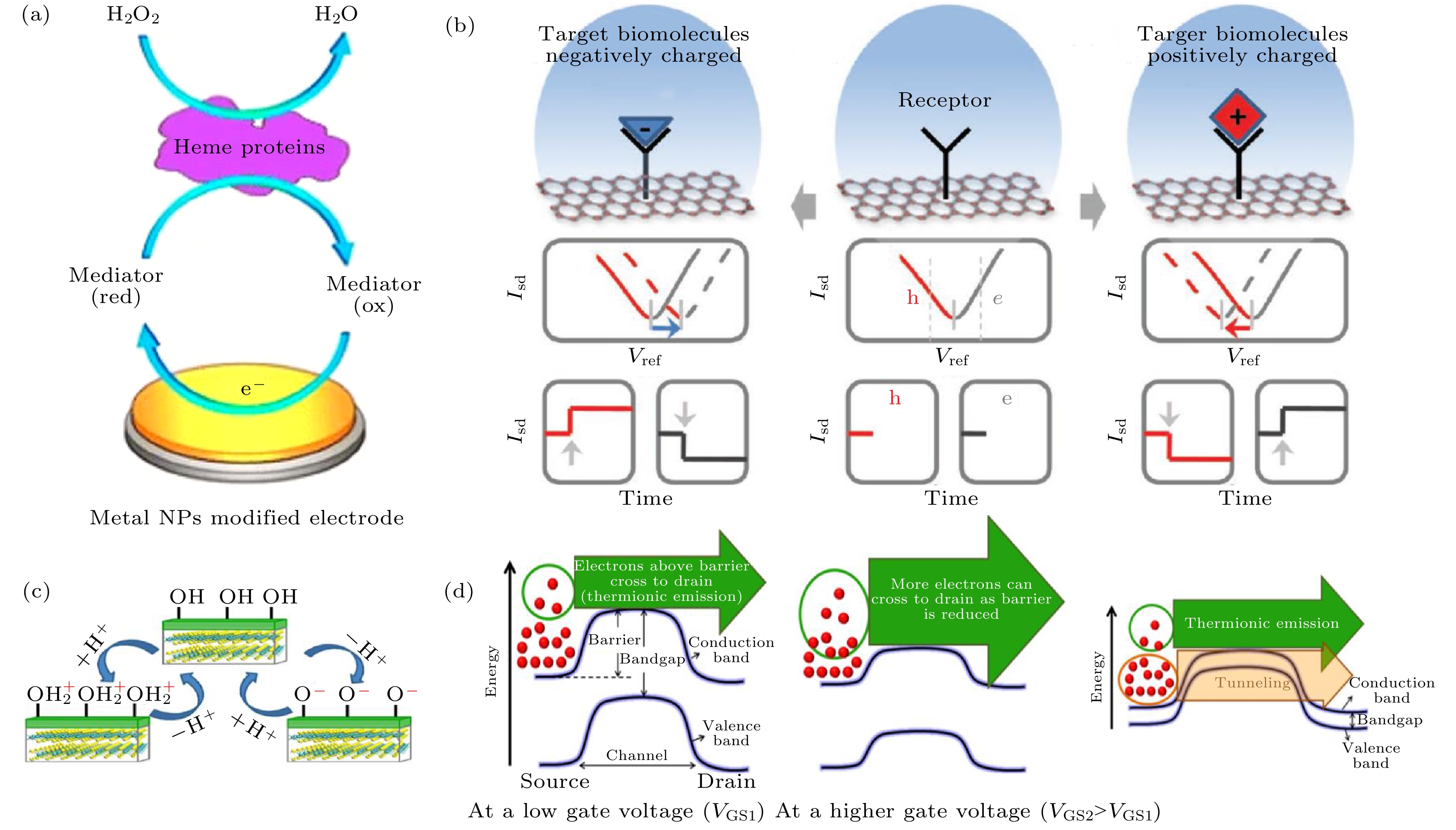
图 1 (a)电化学传感过程示意图[31]; (b)石墨烯场效应晶体管利用场效应检测带电分子传感过程示意图[10]; (c) 硫化钼晶体管检测pH值时吸附离子过程示意图; (d)吸附离子前后, 硫化钼能带示意图; 吸附离子前, 半导体与电极之间形成肖特基势垒, 能量较低的电子无法穿越势垒; 吸附离子后, 相当于给晶体管增加了栅极电压, 使得势垒降低, 能量较低的电子也可以穿越势垒; 除此之外, 还有少部分电子可以以隧穿形式穿过势垒[38]
Figure 1. (a) Schematic of sensing mechanism of electrochemical sensors[31]. (b) Schematic of sensing mechanism of graphene transistor[10]. (c) Illustration of the principle of pH sensing. At lower pH (higher concentration of H+ ions), the OH group on the dielectric surface gets protonated to form
$ {\mathrm{O}\mathrm{H}}_{2}^{+} $ , leading to a positive surface charge on the dielectric, while at higher pH, the OH group gets deprotonated to form O, leading to a negative surface charge on the dielectric. (d) Schematic band diagram illustrating the current flow mechanism in (n-type) field effect transistors (FETs) with the semiconducting layer having a considerable band gap. Only electrons having an energy greater than the barrier height can cross the barrier and contribute to current as shown by the green arrow. At low gate voltage (VGS1), few electrons (within the green circle) can cross the barrier. After the application of a higher gate voltage (VGS2), more electrons (within the green circle) can cross the barrier; In the case where the semiconducting channel has a very small band gap, not only can electrons flow above the top of the barrier, but electrons with lower energies can also tunnel through the barrier, which can increase the leakage current[38].图 2 氮掺杂石墨烯用于葡萄糖氧化酶检测 (a) N掺杂石墨烯示意图, 灰色为碳原子, 蓝色为氮原子, 白色为氢原子; (b) 分别在氮掺杂石墨烯和石墨烯上的葡萄糖氧化酶的循环伏安曲线, 溶液环境为氮气饱和的0.1 mol/L磷酸盐(PBS)溶液; (c) 分别固定在光滑碳电极、石墨烯电极和氮掺杂电极上的葡萄糖氧化酶电流-时间曲线, 电压为–0.15 V, 溶液环境为0.1 mol PBS的溶液(pH值为7.0), 其中葡萄糖每次添加量为0.1 mmol/L[1]
Figure 2. (a) Schematic representation of N-doped graphene. Gray for the carbon atom, blue for the nitrogen atom, and white for the hydrogen atom. (b) Cyclic voltammograms of GOx immobilized on N-doped graphene electrode (solid line) and graphene electrode (dashed line) in N2-saturated 0.1 mol/L phosphate buffered saline (PBS) solution (pH 7.0). Dotted line is for the background. Scan rate is 0.05 V/s. (c) Current-time curves for GOx immobilized on GCE, graphene electrode, and N-doped graphene electrode at –0.15 V in 0.1 mol/L PBS (pH 7.0) with successive addition of 0.1 mmol/L glucose[1].
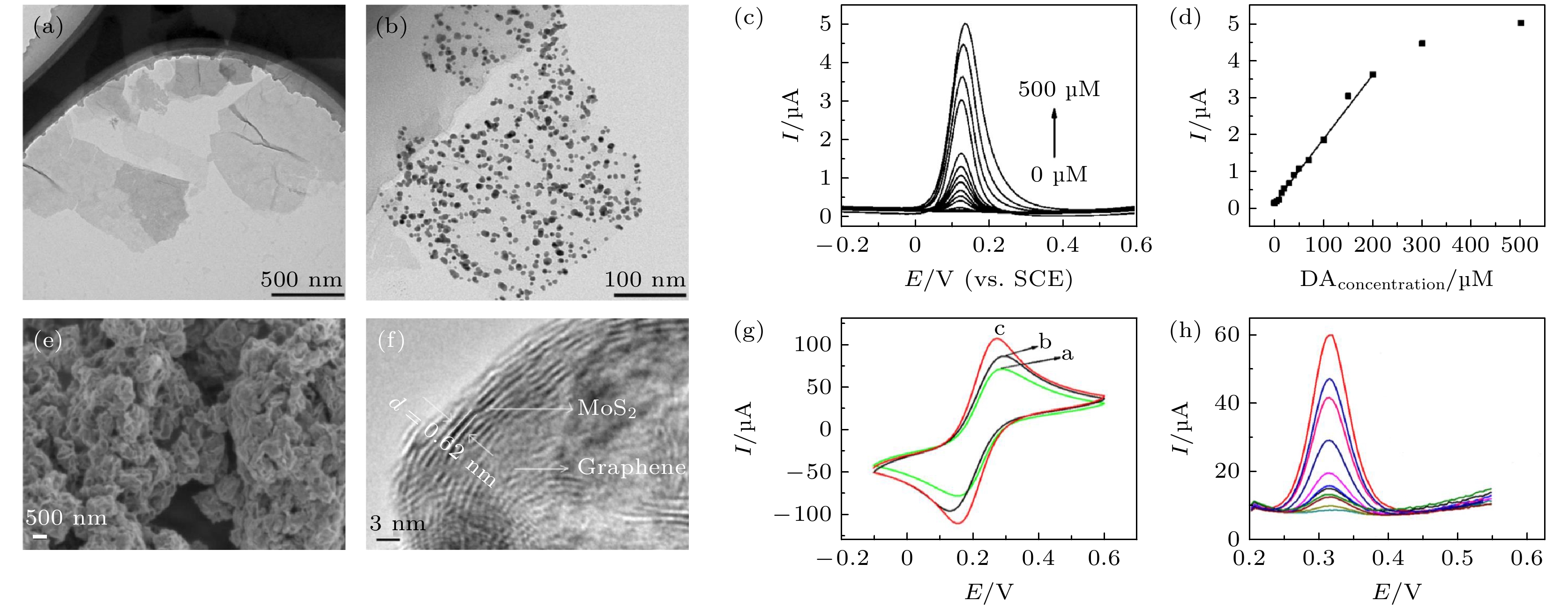
图 3 (a) 硫化钼的隧道电子显微镜(TEM)图; (b) 金纳米颗粒在硫化钼上的TEM图; (c) 基于金纳米颗粒@硫化钼纳米片修饰的光滑碳电极测试不同浓度多巴胺的循环伏安曲线(1 μM = 1 μmol/L); (d) 氧化峰电流和多巴胺浓度的关系曲线[60]; (e) 石墨烯-硫化钼混合物的扫描电子显微镜(SEM)图; (f) 硫化钼-石墨烯高分辨TEM图; (g) 三种不同电极(光滑碳电极、石墨烯在光滑碳电极上、硫化钼-石墨烯在光滑碳电极上)在5 mmol/L
$ {\mathrm{F}\mathrm{e}\left(\mathrm{C}\mathrm{N}\right)}_{6}^{3-/4-} $ 溶液中的伏安循环曲线; (h) 不同浓度的对乙酰氨基酚用硫化钼-石墨烯电极测试的微分脉冲伏安曲线[57]Figure 3. Tunneling electron microscope (TEM) images of the (a) MoS2 and (b) AuNPs@MoS2 nanostructures; (c) differential pulse voltammetric curves of different dopamine (DA) concentrations at AuNPs@MoS2/GCE; (d) plot of oxidation peak currents vs. DA concentrations derived from voltammograms of differential pulse voltammetry (DPV)[60]; (e) scanning electron microscope (SEM) images of MoS2-Gr; (f) high-resolution TEM of MoS2-Gr; (g) CVs of GCE, Gr/GCE and MoS2-Gr/GCE in 5 mmol/L
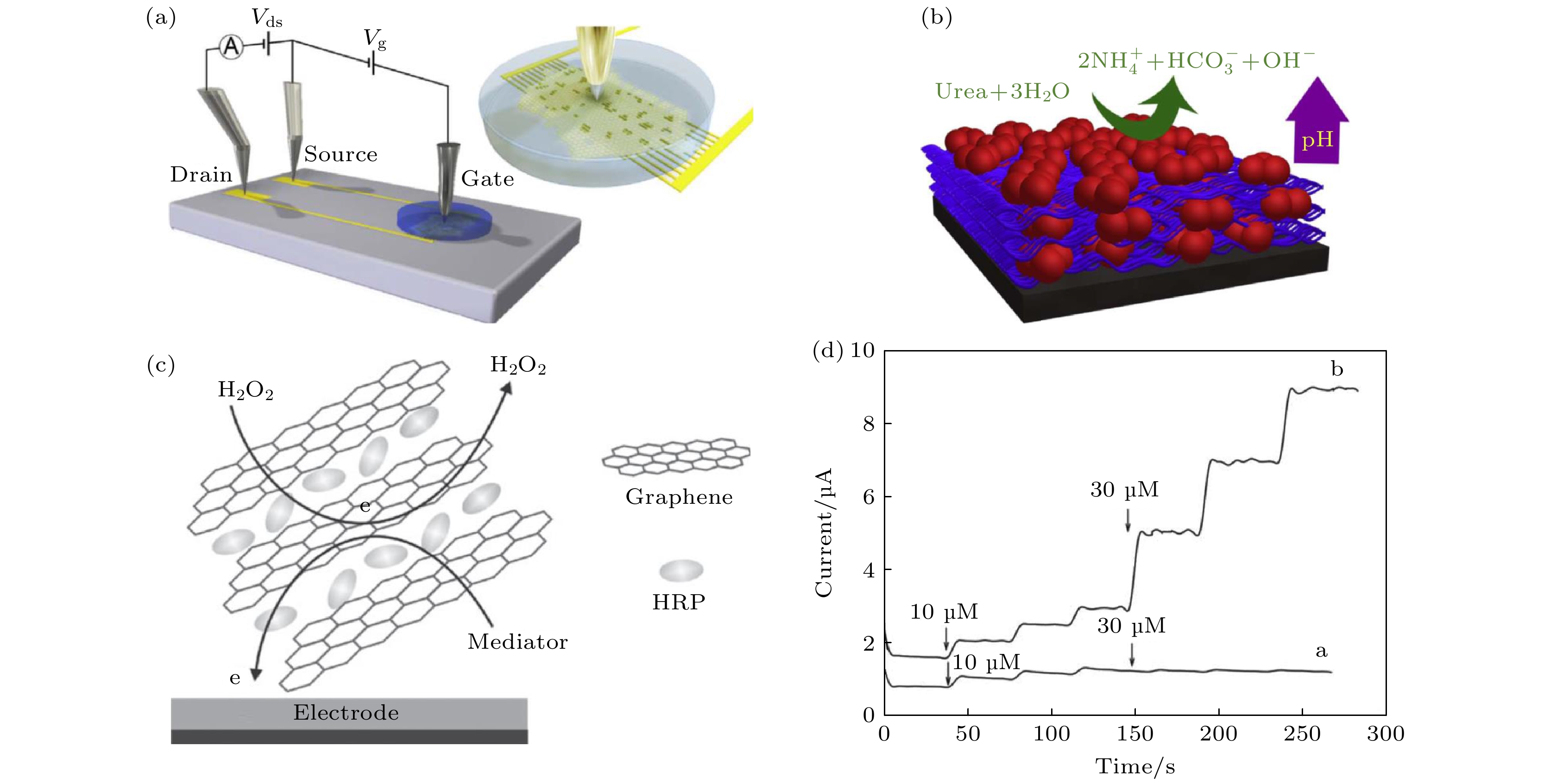
$ {\mathrm{F}\mathrm{e}\left(\mathrm{C}\mathrm{N}\right)}_{6}^{3-/4-} $ containing 0.1 mol/L KCl; (h) DPVs of 0.1, 0.5, 1.0, 3.0, 5.0, 10, 20, 40, 60, 80 and 100 µmol/L acetaminophen (from bottom to top) at MoS2-Gr/GCE in 0.1 mol/L PBS (pH 7.0) [57].图 4 (a) 液体栅极石墨烯场效应晶体管示意图; (b) 由尿素酶连接的多层石墨烯对尿素催化水解反应的示意图[61]; (c) 自组装辣根过氧化物酶-石墨烯纳米片复合材料示意图; (d)玻碳电极和辣根过氧化物酶-石墨烯纳米片复合电极对过氧化氢溶液的动态电学响应[64]
Figure 4. (a) Illustration of the solution gated reduced-graphene-oxide FET and the interdigitated channel; (b) schematic of the urease-polyethylenimine multilayer film and the urease-catalyzed hydrolysis of urea[61]; (c) schematic representation of the self-assembled horseradish peroxidase (HRP)-graphene sheets (GSs) hierarchical bionanocomposites on glass carbon electrode and electron transfer process of the composites on the electrode surface; (d) dynamic amperometric response of the modified electrodes to successive additions of H2O2: SGSs electrode (curve a) and HRP-GSs electrode (curve b) in a stirred 0.1 mol/L PBS (pH 7.0) solution containing 1.0 mmol/L hydroquinone[64].
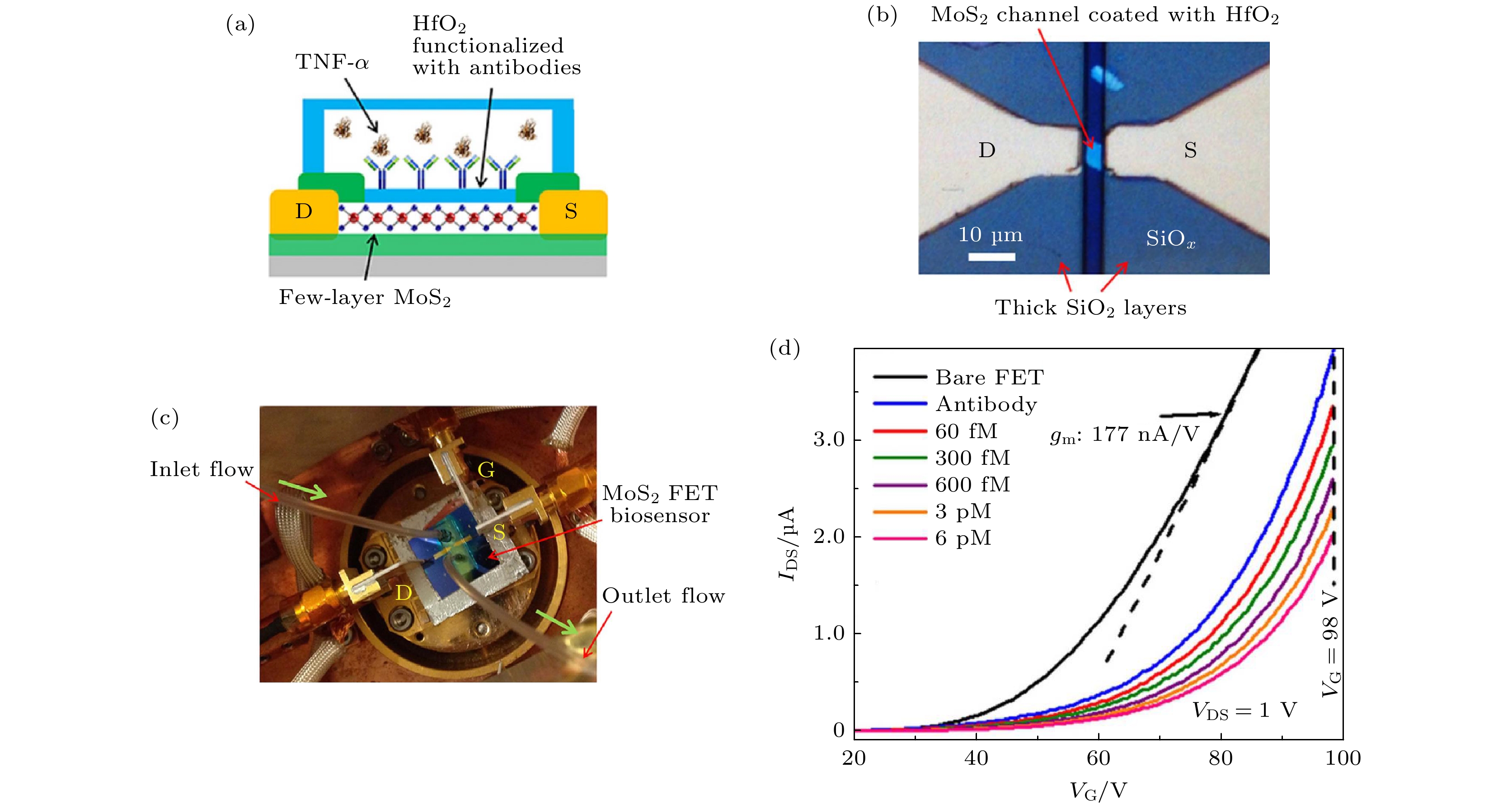
图 5 (a) 硫化钼场效应晶体管生物传感器示意图, 其中功能层用氧化铪和抗体修饰, 用于检测肿瘤坏死因子α (TNF-α); (b) 硫化钼晶体管的光学照片, 沟道长5 μm, 宽6 μm; (c) 集成微流道系统的生物传感器光学照片; (d) 硫化钼晶体管在不同浓度TNF-α下的转移曲线[65]
Figure 5. (a) Functionalization of the HfO2 effective layer with antibody receptors and subsequent TNF-α detection; (b) an exemplary MoS2 transistor with channel length (L) and width (W) of 5 μm and 6 μm, respectively; (c) a transistor biosensor integrated with a microfluidic channel system connected with an inlet/outlet tubing kit, which is driven by a motorized syringe pump; (d) transfer characteristics of an exemplary MoS2 transistor sensor measured at various biodetection stages, following the sequence of bare transistor, antibody functionalization, and inputs of TNF-α solutions with concentrations of 60 fmol/L (fM), 300 fmol/L, 600 fmol/L, 3 pmol/L (pM), and 6 pmol/L[65].
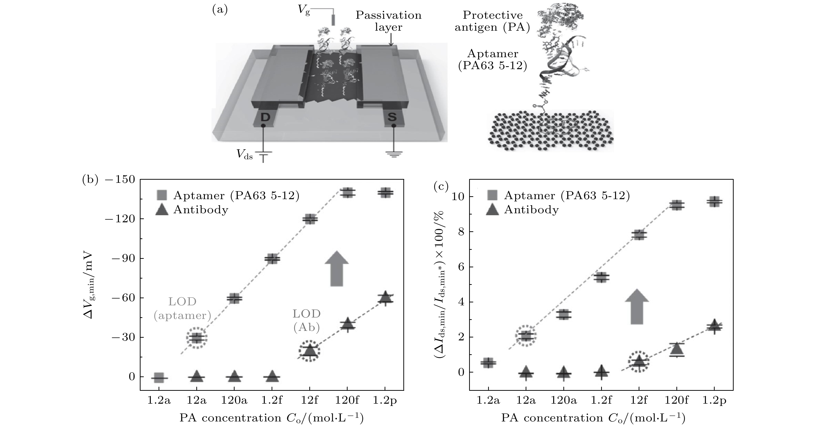
图 6 (a) 适配体修饰在石墨烯场效应晶体管用于抗原检测的示意图; (b) 狄拉克点偏移电压与抗原浓度的关系图; (c) 漏端电流变化值与抗原浓度的关系图, 检测器件为适配体修饰的石墨烯FET和抗体修饰的石墨烯FET[68]
Figure 6. (a) Schematic illustration of the aptamer-immobilized graphene FET for detection of protective antigen (PA); (b) Vg,min shift (ΔVg,min) vs. PA concentration in PBS solutions with different probe molecules. The ΔVg,min value was obtained by calculating the difference in charge neutrality point, Vg,min, as a reference for the device with no binding of PA; (c) change in the minimum source-drain current (Ids,min), ΔIds, min/
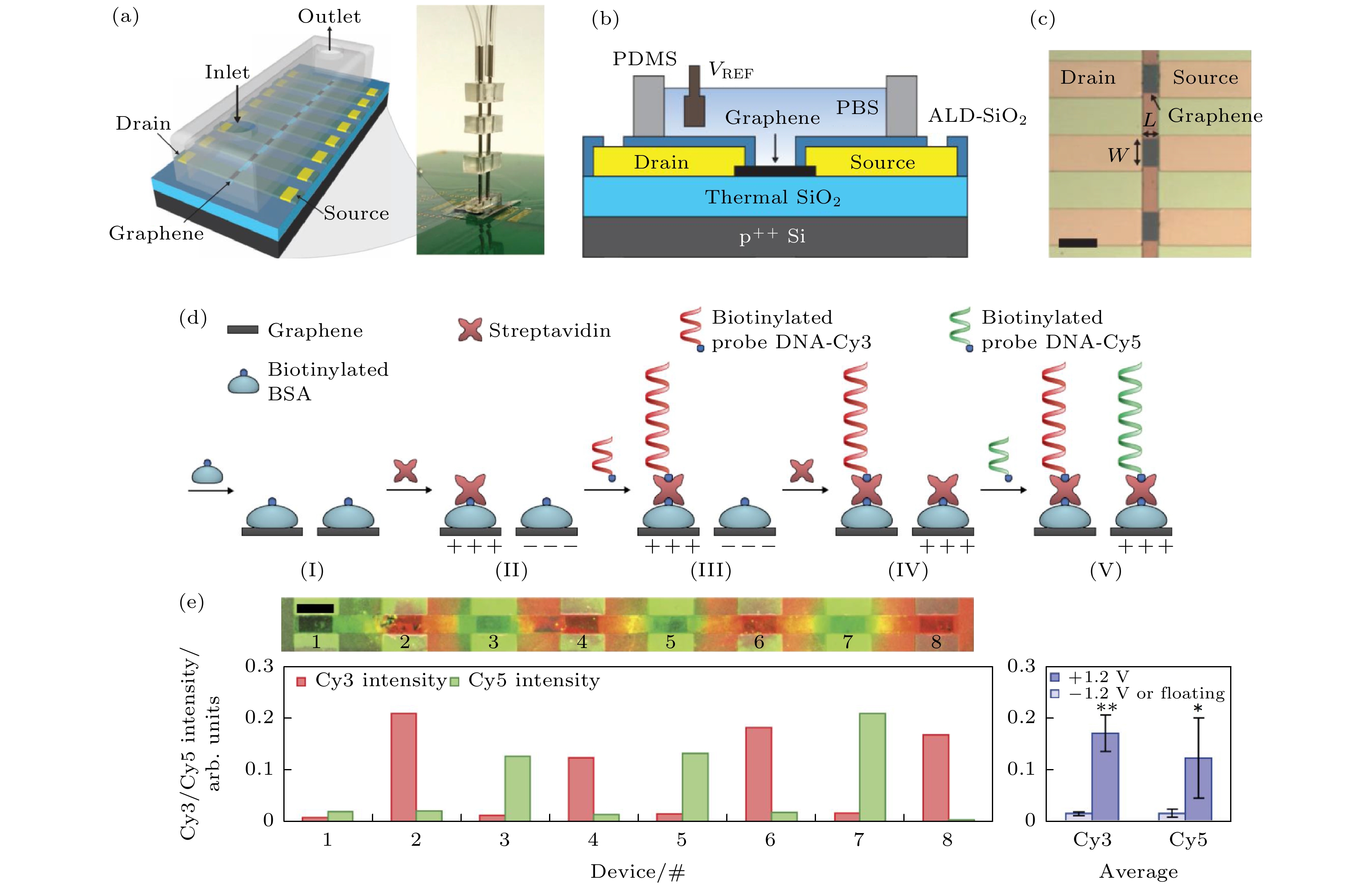
$ I_{\rm ds,min}^* $ × 100 (%) vs. PA concentration. Here,$ I_{\rm ds,min}^* $ is the Ids,min for the device with no binding of PA[68].图 7 (a) 石墨烯场效应晶体管阵列带有一个微流道通道的示意图; (b) 器件界面示意图; (c) 器件光学显微镜图; (d) DNA探针修饰示意图, 两种DNA通过酰化牛血清蛋白和链霉亲和素连接到石墨烯表面, 其中一种DNA修饰荧光分子Cy3, 另外一种修饰荧光分子Cy5. 先分别在奇数位点施加+1.2 V电压, 偶数位点施加–1.2 V电压, 将带有Cy3的DNA探针固定到奇数位点; 然后在偶数位点加+1.2 V偏压, 奇数位点不加偏压, 带有Cy5的DNA探针被固定到偶数位点上; (e)带有Cy3和Cy5的FET阵列的共聚焦荧光成像图, 其中Cy3发出红色荧光, Cy5发出绿色荧光[70]
Figure 7. (a) Illustration and image of an 8-graphene-electrode/FET array with a microfluidic channel on top. This entire device sits on a printed circuit board. (b) Cross-sectional illustration of an individual graphene site. (c) Optical micrograph of a portion of a fabricated graphene array. For an individual graphene site, W = 90 μm and L = 45 μm (scale bar, 120 μm). (d) During the immobilization of Cy3-labelled probe DNA and associated streptavidin, even- (odd-) numbered sites are biased at 1.2 V (–1.2 V) (20 and 120 s for streptavidin and Cy3-labelled probe DNAs, respectively). During the subsequent immobilization of Cy5-labelled probe DNAs and associated streptavidin, the even- (odd-) numbered sites are left unbiased (biased at 1.2 V), with the same timing scheme as before. (e) Confocal fluorescence image (false coloured) of the array with Cy3 and Cy5 probe DNAs shown, respectively, as red and green, and the corresponding normalized fluorescence intensity. The averaged fluorescence intensities across the four even-numbered and four odd-numbered graphene sites with Cy5 intensity are normalized to the maximum Cy3 intensity; *P < 0.05; **P < 0.01; error bars represent ± 1 s.d. Scale bar, 100 μm[70].
图 8 磷脂膜在二氧化硅和石墨烯上的示意图 (a) 部分区域单层、部分区域双层的磷脂膜在二氧化硅上; (b) 双层磷脂膜修饰在石墨烯表面; (c) 在石墨烯衬底上的单层磷脂分子被牛血清分子包围; (d) 链霉亲和素被特异性绑定在生物酰化的基团上, 牛血清蛋白阻止了链霉亲和素的非特异性绑定[71]
Figure 8. Proposed membrane organization on silicon dioxide and graphene. 1, 2-dioleoyl-sn-glycero-3-phosphocholine (DOPC) headgroups are marked in red, Biotin-PE headgroups in green. (a) Base monolayer and additional bilayer on silicon dioxide in air; (b) single bilayer on graphene in air and (c) monolayer of phospholipids on graphene surrounded by bull serum albumin (BSA) layer under water; (d) streptavidin can later be bound to the biotinylated headgroups of the phospholipids from solution with BSA and DOPC preventing unspecific binding to the substrate[71].
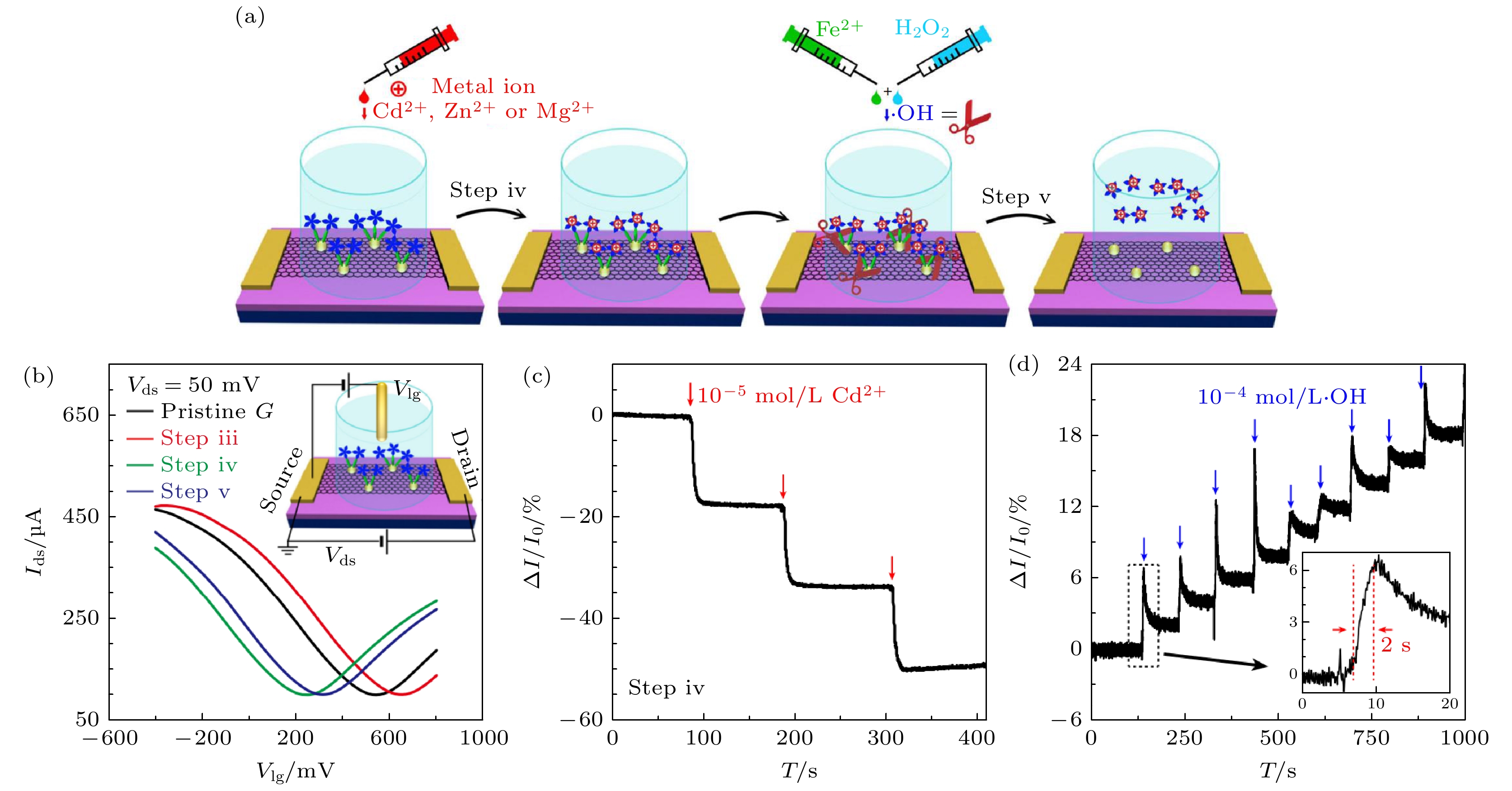
图 9 (a) 石墨烯FET传感器传感机制示意图; (b) 液栅晶体管I-V曲线, 四条曲线分别为纯石墨烯晶体管转移曲线(黑色), 经历金纳米颗粒/半胱胺-原卟啉修饰石墨烯FET的转移曲线(红色), 经历金属离子修饰后石墨烯FET的转移曲线(10–4 mol/L Cd+, 绿色), 经历剪切反应后石墨烯FET的转移曲线(10–4 mol/L·OH, 蓝色); (c), (d) 石墨烯/金/半胱胺-原卟啉传感器对铬离子和羟基的实时响应曲线 (1 M = 1 mol/L)[72]
Figure 9. Detection performance and mechanism of the FET sensor: (a) Schematic diagram of the ·OH detection; (b) liquid gate transfer curves of a FET device of pristine graphene (black), after decoration of gold nanoparticle/cysteamine-protoporphyrin (red), after metallic ions (10–4 mol/L Cd2+, green), and after shear reaction (10–4 mol/L ·OH, blue), when liquid gate voltage (Vg) varies from –400 to 800 mV; (c), (d) real-time electrical responses of a graphene/Au/Cys-PP FET device upon successive addition of Cd2+ and subsequent ·OH[72].
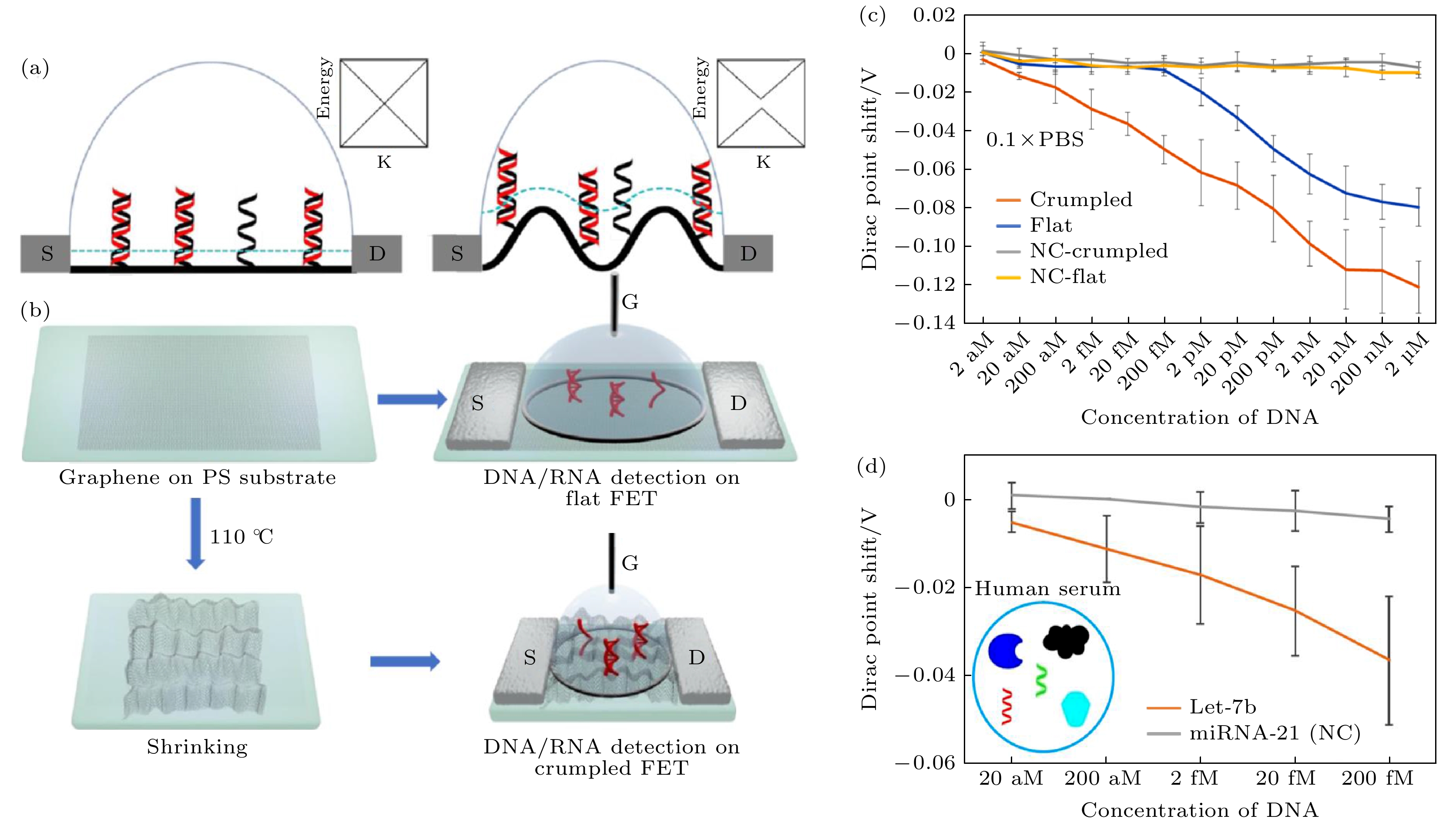
图 10 (a)平坦石墨烯晶体管DNA传感器和褶皱石墨烯晶体管DNA传感器的截面示意图, 黑色为探针DNA, 红色为目标DNA链, 蓝色线代表德拜长度, 在凹陷结构中的DNA链有更长的部分在德拜长度以内; (b)平坦石墨烯晶体管和褶皱石墨烯晶体管的制作流程示意图; (c)狄拉克点偏移量与被测DNA浓度关系图 (1 M = 1 mol/L); (d)在人血清中, 石墨烯狄拉克点偏移与被测DNA浓度关系图[73]
Figure 10. (a) Cross-sectional scheme of the flat (left) and crumpled (right) graphene FET DNA sensor. Probe (black) and target (red) DNA strands are immobilized on the surface of graphene. The blue dot lines represent Debye length in the ionic solution and the length is increased at the convex region of the crumpled graphene, thus more area DNA is inside the Debye length, which makes the crumpled graphene more electrically susceptible to the negative charge of DNA. (b) Fabrication of FETs and experimental process flow. Graphene on pre-strained PS substrate was annealed at 110 °C to shrink the substrate and crumple the graphene. Then source and drain electrodes were applied and solution-top gate was used. In case of flat graphene FET, the annealing process was omitted. (c) Dirac voltage shift of the FET sensor with detection of hybridization using DNA probe. NC is non-complementary control sequences used in the experiments. (d) Dirac voltage shift of the FET sensor with miRNA detection of hybridization. Target RNA spiked in human serum was treated on the FET sensor. Human serum is complex mixture of biological components[73].
图 11 (a) 石墨烯超表面设计, 将石墨烯沉积在金表面; 为了激发石墨烯-金界面处表面等离激元极化, 一束光通过一个玻璃棱镜照射在50 nm金薄膜上, 然后反射到另外一个面; 金纳米颗粒连接到DNA上作为SPR增强的标签; (b) 光的反射率(黑线)和相位(红线)作为光照射在石墨烯-金界面处入射角的函数, 其中, 相位在SPR曲线最小值处经历了一个奇变点; (c) 对比了纯石墨烯和石墨烯加金纳米颗粒(石墨烯先利用π-π相互作用与DNA连接, 然后将金纳米颗粒连接到DNA上, 从而增强DNA检测信号)两种器件对单链DNA浓度检测的信号强度[76]
Figure 11. Designs of graphene-gold metasurface architectures. (a) Basic architecture with a layer of graphene deposited on the gold surface. To excite surface plasmon polariton over the graphene-gold interface, a light beam is typically passed through a glass prism and reflected from a 50 nm gold film deposited on one of its facets. (b) Calculated reflectivity (black) and phase (red) of light as functions of the angle of light incidence of the gold-graphene interface, corresponding to maximum probing field. Phase experiences a sharp singularity in the minimum of SPR curve. (c) Response and magnitude of enhancement (in the bracket) obtained with (circles) and without (squares) exposing the monolayer graphene-coated sensing film to positive-charged Au NPs after ssDNA[76].
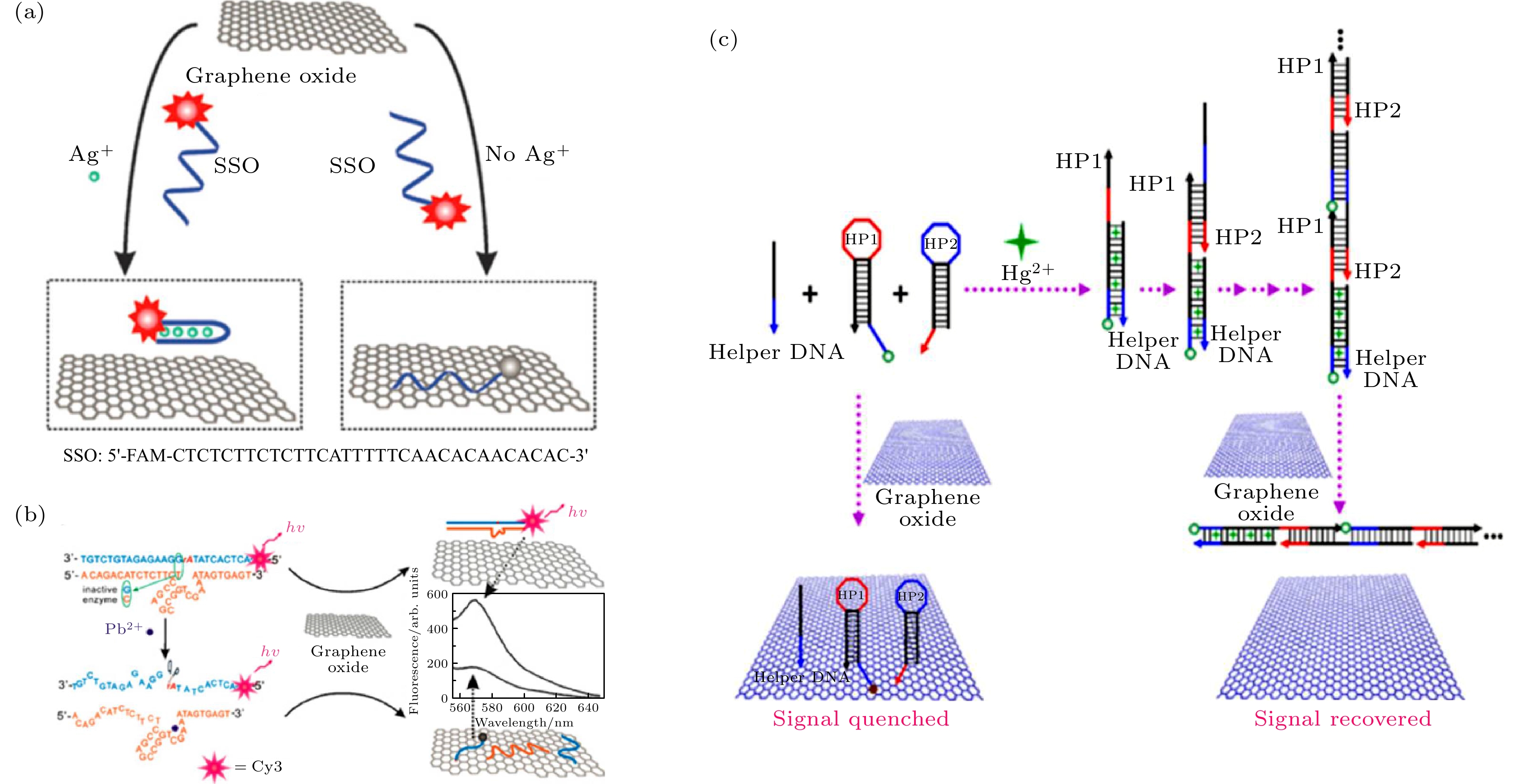
图 12 (a) 银离子荧光传感器示意图, 特异性识别银离子的DNA链在和银离子相互作用后导致DNA链构型改变, 从而DNA链从氧化石墨烯上脱附, DNA所携带的荧光分子产生荧光[79]; (b) 铅离子调节DNA酶与氧化石墨烯的相互作用的示意图[81]; (c) 汞离子探测机制示意图[82]
Figure 12. (a) Schematic illustration of the fluorescence sensor for Ag+ ions based on the target-induced conformational change of a SSO and the interactions between the fluorogenic silver-specific oligonucleotide probe and graphene oxide (GO)[79]. (b) Schematic for the Pb2+-modulated interactions between DNAzyme and GO. Inset is the fluorescence spectrum of a mixture of DNAzyme and GO upon interaction with 0 mol/L (top curve) and 2 mmol/L (bottom curve) of Pb2+ in a Tris-HCl buffer (50 mmol/L, pH = 7.4) solution containing 50 mmol/L NaCl[81]. (c) Schematic of the proposed detection mechanism (for clarity, pristine graphene is used to represent GO)[82].
-
[1] Wang Y, Shao Y, Matson D, Li J, Lin Y 2010 ACS Nano 4 1790
 Google Scholar
[2] Zhu C, Zhai J, Wen D, Dong S 2012 J. Mater. Chem. 22 6300
 Google Scholar
[3] Guo S, Dong S 2011 Chem. Soc. Rev. 40 2644
 Google Scholar
[4] Huang X, Tan C, Yin Z, Zhang H 2014 Adv. Mater. 26 2185
 Google Scholar
[5] Sudibya H G, He Q, Zhang H, Chen P 2011 ACS Nano 5 1990
 Google Scholar
[6] Huang X, Zeng Z, Bao S, Wang M, Qi X, Fan Z, Zhang H 2013 Nat. Commun. 4 1444
 Google Scholar
[7] Novoselov K S, Geim A K, Morozov S V, Jiang D, Zhang Y, Dubonos S V, Grigorieva I V, Firsov A A 2004 Science 306 666
 Google Scholar
[8] Ohno Y, Maehashi K, Matsumoto K 2010 J. Am. Chem. Soc. 132 18012
 Google Scholar
[9] Heller I, Chatoor S, Mannik J, Zevenbergen M A G, Dekker C, Lemay S G 2010 J. Am. Chem. Soc. 132 17149
 Google Scholar
[10] Fu W, Nef C, Tarasov A, Wipf M, Stoop R, Knopfmacher O, Weiss M, Calame M, Schonenberger C 2013 Nanoscale 5 12104
 Google Scholar
[11] An G, Li S, Cheng T, Yan X, Zhang X, Zhou X, Yuan Z 2019 Plasmonics 14 155
 Google Scholar
[12] Arasu P T, Noor A S M, Shabaneh A A, Yaacob M H, Lim H N, Mahdi M A, 2016 Opt. Commun. 380 260
 Google Scholar
[13] Tang Y, Song H, Su Y, Lv Y 2013 Anal. Chem. 85 11876
 Google Scholar
[14] Ma T Y, Tang Y, Dai S, Qiao S Z 2014 Small 10 2382
 Google Scholar
[15] Alharbi R, Irannejad M, Yavuz M 2017 Plasmonics 12 783
 Google Scholar
[16] Song Y J, Wei W L, Qu X G 2011 Adv. Mater. 23 4215
 Google Scholar
[17] Jiang L, Fu W, Birdja Y Y, Koper M T M, Schneider G F 2018 Nat. Commun. 9 793
 Google Scholar
[18] Ren X, Ma H, Zhang T, Zhang Y, Yan T, Du B, Wei Q 2017 ACS Appl. Mater. Interfaces 9 37637
 Google Scholar
[19] Yang J, Ma M Z, Li L Q, Zhang Y F, Huang W, Dong X C 2014 Nanoscale 6 13301
 Google Scholar
[20] Xia J L, Chen F, Li J H, Tao N J 2009 Nat. Nanotechnol. 4 505
 Google Scholar
[21] Bockris J O, Gileadi E, Muller K 1966 J. Chem. Phys. 44 1445
 Google Scholar
[22] Aguilella V M, Pellicer J, Aguilella-Arzo M 1999 Langmuir 15 6156
 Google Scholar
[23] Bergveld P 2003 Sens. Actuators, B 88 1
 Google Scholar
[24] Bergveld P 1970 IEEE Trans. Biomed. Eng. 17 70
 Google Scholar
[25] Sorgenfrei S, Chiu C Y, Johnston M, Nuckolls C, Shepard K L 2011 Nano Lett. 11 3739
 Google Scholar
[26] Zhang M, Liao C Z, Mak C H, You P, Mak C L, Yan F 2015 Sci. Rep. 5 8311
 Google Scholar
[27] Kwak Y H, Choi D S, Kim Y N, Kim H, Yoon D H, Ahn S S, Yang J W, Yang W S, Seo S 2012 Biosens. Bioelectron. 37 82
 Google Scholar
[28] You X, Pak J J 2014 Sens. Actuators, B 202 1357
 Google Scholar
[29] Cagang A A, Abidi I H, Tyagi A, Hu J, Xu F, Lu T J, Luo Z T 2016 Anal. Chim. Acta 917 101
 Google Scholar
[30] Liao C Z, Zhang M, Niu L Y, Zheng Z J, Yan F 2013 J. Mater. Chem. B 1 3820
 Google Scholar
[31] Chen S, Yuan R, Chai Y, Hu F 2013 Microchimi. Acta 180 15
 Google Scholar
[32] Lu M, Deng Y, Luo Y, Lv J P, Li T B, Xu J, Chen S W, Wang J Y 2019 Anal. Chem. 91 888
 Google Scholar
[33] Yang J, Ye H, Zhao F Q, Zeng B H 2016 ACS Appl. Mater. Interfaces 8 20407
 Google Scholar
[34] Ling P, Qian C, Yu J J, Gao F 2020 Biosens. Bioelectron. 149 111838
 Google Scholar
[35] Dai L, Li Y, Wang Y, Luo X L, Wei D, Feng R, Yan T, Ren X, Du B, Wei Q 2019 Biosens. Bioelectron. 132 97
 Google Scholar
[36] Xu Z, Yang L, Xu C 2015 Anal. Chem. 87 3438
 Google Scholar
[37] Maehashi K, Sofue Y, Okamoto S, Ohno Y, Inoue K, Matsumoto K 2013 Sens. Actuators, B 187 45
 Google Scholar
[38] Sarkar D, Liu W, Xie X, Anselmo Aaron C, Samir M, Banerjee K 2014 ACS Nano 8 3992
 Google Scholar
[39] 杨志宇, 代宁宁, 吕瑞涛, 黄正宏, 康飞宇 2015 新型炭材料 30 511
 Google Scholar
Yang Z Y, Dai N N, Lu R T, Huang Z H, Kang F Y 2015 New Carbon Mater. 30 511
 Google Scholar
[40] Chang J B, Zhou G H, Christensen E R, Heideman R, Chen J H 2014 Anal. Bioanal. Chem. 406 3957
 Google Scholar
[41] Zhang T, Cheng Z G, Wang Y B, Li Z J, Wang C X, Li Y B, Fang Y 2010 Nano Lett. 10 4738
 Google Scholar
[42] Wang C Y, Cui X Y, Li Y, Li H B, Huang L, Bi J, Luo J, Ma L Q, Zhou W, Cao Y, Wang B G, Miao F 2016 Sci. Rep. 6 21711
 Google Scholar
[43] Zhou G H, Chang J B, Cui S M, Pu H H, Wen Z H, Chen J H 2014 ACS Appl. Mater. Interfaces 6 19235
 Google Scholar
[44] Mannoor M S, Tao H, Clayton J D, Sengupta A, Kaplan D L, Naik R R, Verma N, Omenetto F G, McAlpine M C 2012 Nat. Commun. 3 763
 Google Scholar
[45] Huang H, Tao L, Liu F, Ji L, Hu Y, Cheng M M C, Chen P Y, Akinwande D 2016 Microsyst. Nanoeng. 2 16018
 Google Scholar
[46] Mao S, Chang J B, Zhou G H, Chen J H 2015 Small 11 5336
 Google Scholar
[47] Viswanathan S, Narayanan T N, Aran K, et al. 2015 Mater. Today 18 513
 Google Scholar
[48] Clarke W L, Cox D, Gonderfrederick L A, Carter W, Pohl S L 1987 Diabetes Care 10 622
 Google Scholar
[49] Zeng Z, Yin Z, Huang X, Li H, He Q, Lu G, Boey F, Zhang H 2011 Angew. Chem. Int. Ed. 50 11093
 Google Scholar
[50] Schwinghammer K, Mesch M B, Duppel V, Ziegler C, Senker J, Lotsch B V 2014 J. Am. Chem. Soc. 136 1730
 Google Scholar
[51] Cao L, Meziani M J, Sahu S, Sun Y P 2013 Acc. Chem. Res. 46 171
 Google Scholar
[52] Ma Y C, Foster A S, Krasheninnikov A V, Nlemlem R M 2005 Phys. Rev. B 72 205416
 Google Scholar
[53] Zhou C W, Kong J, Yenilmez E, Dai H J 2000 Science 290 1552
 Google Scholar
[54] Huang K J, Wang L, Liu Y J, Gan T, Liu Y M, Wang L L 2013 Electrochim. Acta 107 379
 Google Scholar
[55] Zhang Y, Sun R, Luo B, Wang L 2015 Electrochim. Acta 156 228
 Google Scholar
[56] Yeh M H, Li Y S, Chen G L, Lin L Y, Li T J, Chuang H M, Hsieh C Y, Lo S C, Chiang W H, Ho K C 2015 Electrochim. Acta 172 52
 Google Scholar
[57] Borowiec J, Zhang J 2015 J. Electrochem. Soc. 162 B332
 Google Scholar
[58] Su S, Sun H, Xu F, Li H, Wen Y 2013 Electroanalysis 25 11
 Google Scholar
[59] Huang J W, Dong Z P, Li Y R, Li J, Tang W J, Yang H D 2013 Mater. Res. Bull. 48 4544
 Google Scholar
[60] Huang K J, Wang L, Li J, Liu Y M 2013 Sens. Actuators, B 178 671
 Google Scholar
[61] Piccinini E, Bliem C, Ciril R R, Battaglini F, Azzaroni O, Knoll W 2017 Biosens. Bioelectron. 92 661
 Google Scholar
[62] Huang Y X, Dong X C, Shi Y M, Li C M, L. Li J, Chen P 2010 Nanoscale 2 1485
 Google Scholar
[63] Kavitha T, Gopalan A I, Lee K P, Park S Y 2012 Carbon 50 2994
 Google Scholar
[64] Zeng B Q, Cheng J S, Tang L H, Liu X F, Liu Y Z, Li J H, Jiang J H 2010 Adv. Funct. Mater. 20 3366
 Google Scholar
[65] Nam H, Oh B R, Chen P 2015 Sci. Rep. 5 10546
 Google Scholar
[66] Mao S, Lu G H, Yu K H, Bo Z, Chen J H 2010 Adv. Mater. 22 3521
 Google Scholar
[67] Chen Y T, Ren R, Pu H H, Chang J B, Mao S, Chen J H 2017 Biosens. Bioelectron. 89 505
 Google Scholar
[68] Kim D J, Park H C, Sohn I Y, Jung J H, Yoon O J, Park J S, Yoon M Y, Lee N E 2013 Small 9 3352
 Google Scholar
[69] Gao A R, Zou N L, Dai P F, Lu N, Li T, Wang Y L, Zhao J L, Mao H J 2013 Nano Lett. 13 4123
 Google Scholar
[70] Xu G Y, Abbott J, Qin L, Yeung K Y M, Song Y, Yoon H, Kong J, Ham D 2014 Nat. Commun. 5 4866
 Google Scholar
[71] Michael H, Antonios O, Thanasis G, Harald F Aravind V 2013 Nat. Commun. 4 2591
 Google Scholar
[72] Wang Z, Yi K Y, Lin Q Y, Yang L, Chen X S, Chen H, Liu Y Q, Wei D C 2019 Nat. Commun. 10 1544
 Google Scholar
[73] Hwang M T, Heiranian M, Kim Y, et al. 2020 Nat. Commun. 11 1543
 Google Scholar
[74] Aksimsek S, Jussila H, Sun Z 2018 Opt. Commun. 428 233
 Google Scholar
[75] Al-rekabi S H, Kamil Y M, Bakar M H A, Fen Y W, Lim H N, Kanagesan S, 2019 Opt. Laser Technol. 111 417
 Google Scholar
[76] Zeng S, Sreekanth K V, Shang J, Yu T, Chen C K, Yin F, Baillargreat D, Coquet P, Ho H P, Kabashin A V, Yong K T 2015 Adv. Mater. 27 6163
 Google Scholar
[77] Kravets V G, Schedin F, Jalil R, Britnell L, Gorbachev R V, Ansell D, Thackray B, Novoselov K S, Geim A K, Kabashin A V, Grigorenko A N 2013 Nat. Mater. 12 304
 Google Scholar
[78] Daniel R, Odeta L, Davide J, Dordaneh E, Javier G D A, Valerio P, Hatice A 2015 Science 6244 165
 Google Scholar
[79] Wen Y, Xing F, He S, Song S, Wang L, Long Y, Li D, Fan C 2010 Chem. Commun. 46 2596
 Google Scholar
[80] Cui X, Zhu L, Wu J, Hou Y, Wang P, Wang Z, Yang M 2015 Biosens. Bioelectron. 63 506
 Google Scholar
[81] Wen Y, Peng C, Li D, Zhuo L, He S, Wang L, Huang Q, Xu Q H, Fan C 2011 Chem. Commun. 47 6278
 Google Scholar
[82] Huang J, Gao X, Jia J, Kim J K, Li Z 2014 Anal. Chem. 86 3209
 Google Scholar
Catalog
Metrics
- Abstract views: 21217
- PDF Downloads: 480
- Cited By: 0



 DownLoad:

