-
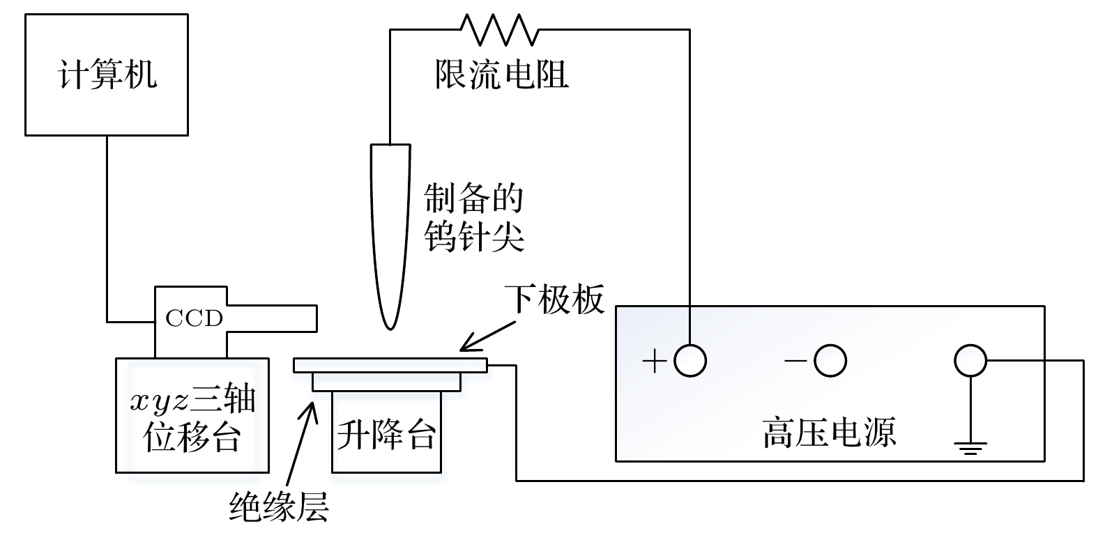
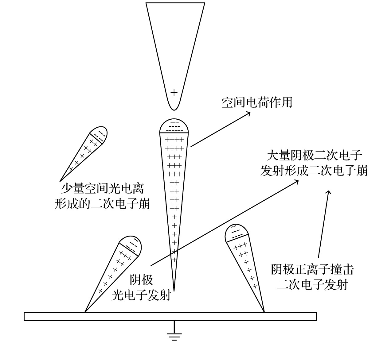
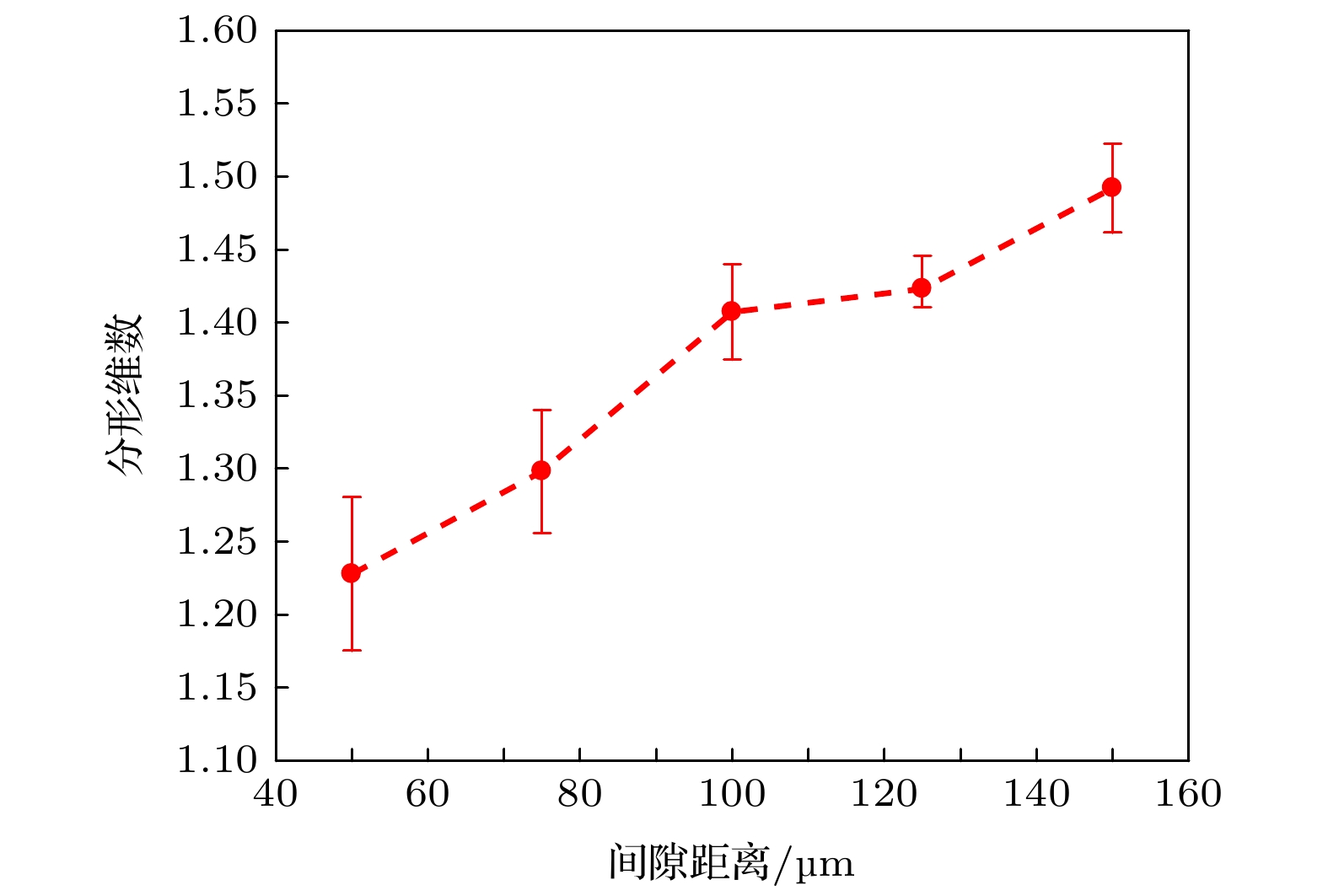
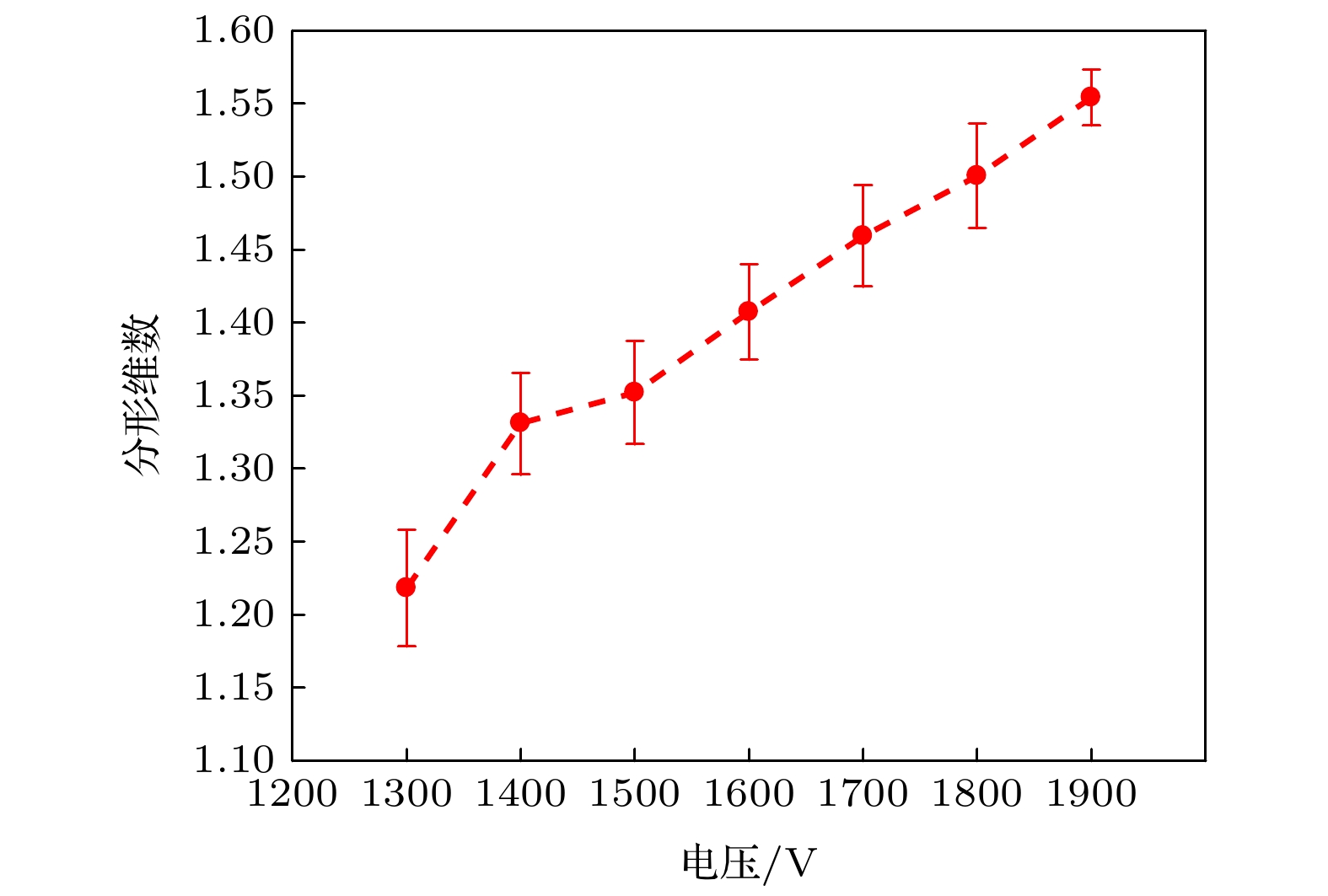
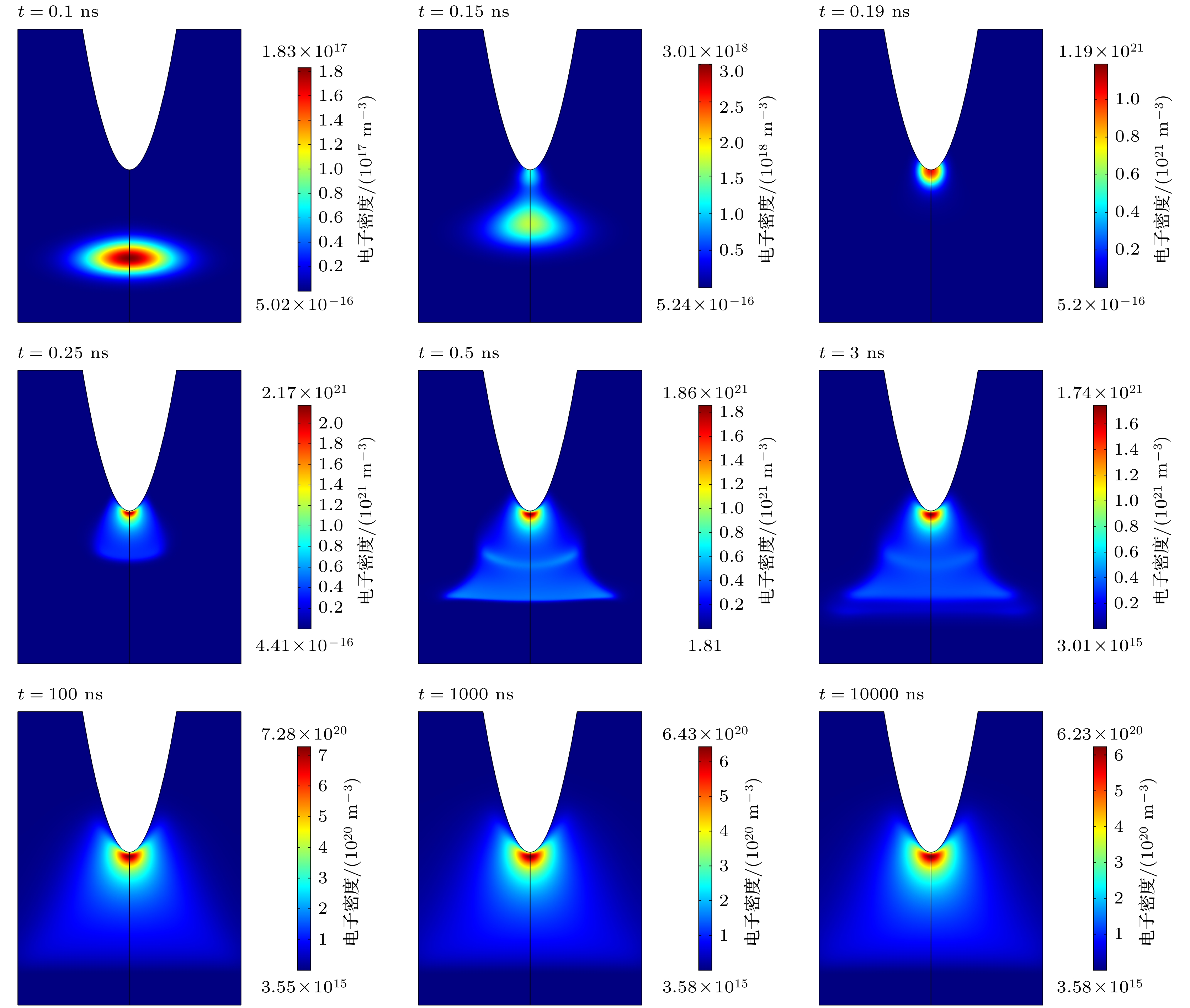
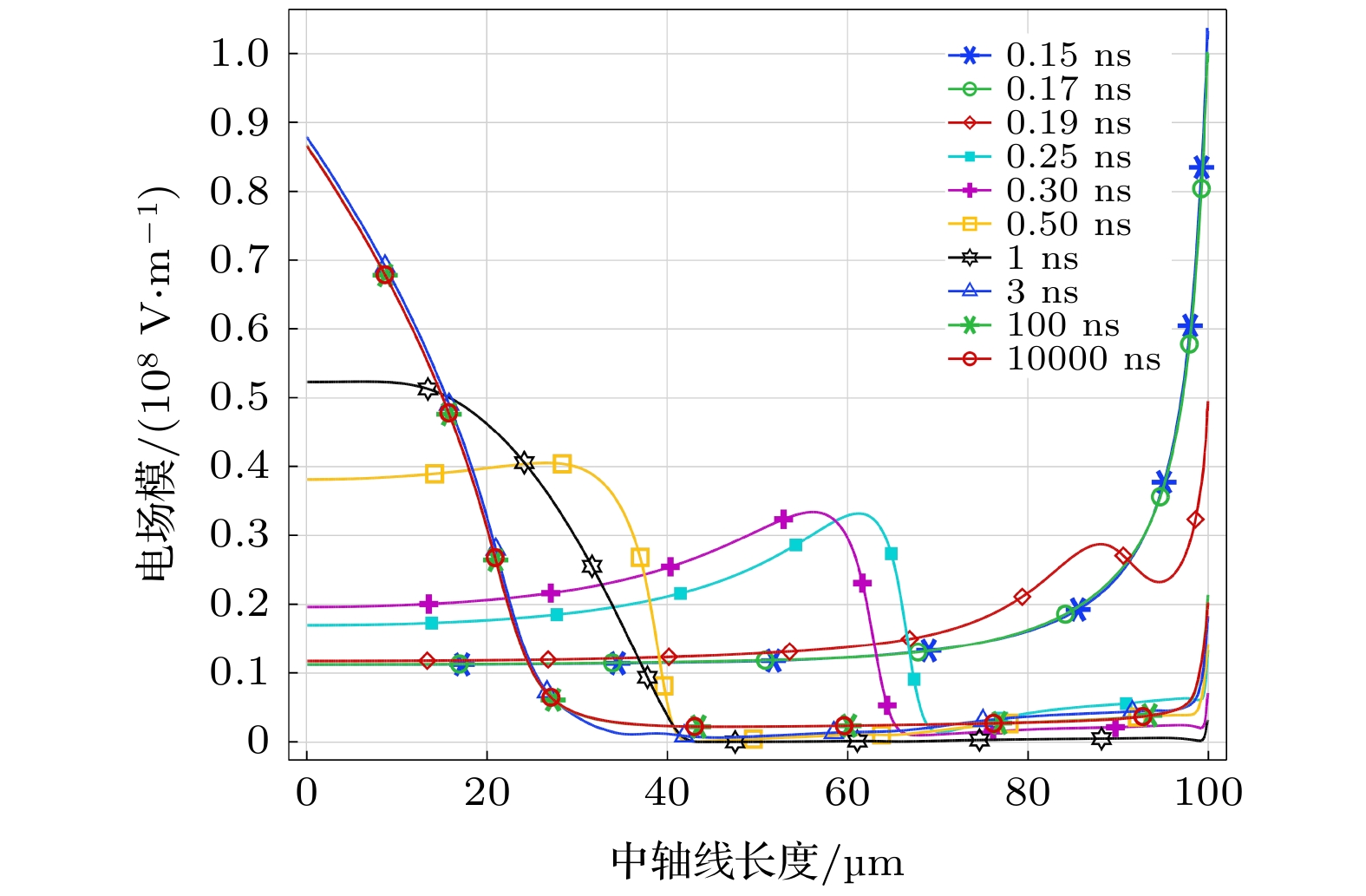
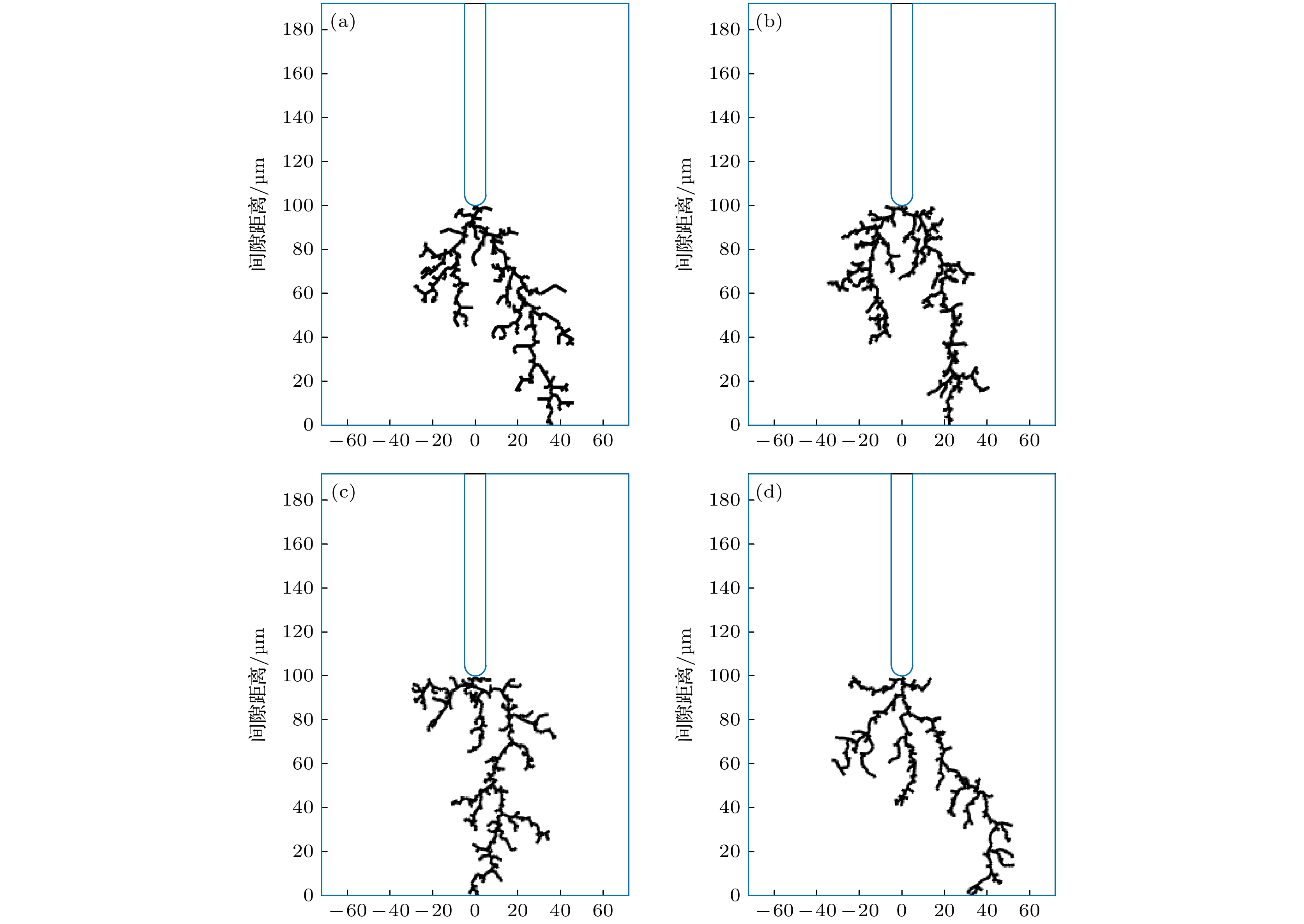
Micro-gap discharge is a form of gas discharge in which the discharge gap is on the order of sub-millimeters orless. To study the initial path of micro-gap discharge and the mechanism and law of particle density change during discharge, in this paper a micro-gap discharge experiment and discharge image acquisition device under atmospheric pressure is built and the COMSOL simulation software is used to simulate the electron density and space charge in the process of micro-gap air discharge. Furthermore, the MATLAB software is used to calculate the fractal dimension and probability development index of micro-gap discharge. The air discharge phenomena produced by applying positive DC voltage to needle tip at atmospheric pressure and room temperature with gap distance ranging from 50 μm to 150 μm are studied. It is found experimentally that there are twists and turns in the discharge channel, and the number of bifurcations in the discharge process with a short gap is less than that with a long gap. Observation of the micro-gap air discharge process with a gap of 100 μm under atmospheric pressure shows that the discharge process is divided into the following three processes: needle tip corona, corona breakdown streamer, and spark discharge channel. Based on the analyses of these experimental results, it can be concluded that the discharge mechanism follows Thomson's theory, supplemented by the streamer theory. The cathode secondary electron emission (including positive ions colliding with the cathode and photoelectron emission) and the space charge distortion electric field form a secondary electron avalanche to maintain the discharge together. The seed electrons formed by a small amount of space photoionization also form an electron avalanche under the action of the space charge distortion electric field. There are tortuous sections in the discharge channel, but the number of branches is small and the degree of tortuosity is low. Therefore, there are weak streamer forms. The discharge channel is tortuous and branched, but the number of bifurcations is relatively small, and the tortuousness is low. In addition, it is also found that a sheath is formed at the cathode, the distortion of electric field is 3–8 times that of original electric field, and the electron density reaches 2 × 10²¹ m–3 during discharge, obtained from the COMSOL simulation. Meanwhile, the fractal theory simulation is used to simulate the micro-gap discharge. In the process of research, the fractal dimension is found to be proportional to the voltage and the gap distance. When the probability development index η = 1.18–1.3, the fractal dimension of the simulated discharge process is closer to the experimental result. The findings in this paper lay the foundation for further exploring the discharge theory of sub-micro- and nano-scaled gaps.
-
Keywords:
- micron gap discharge /
- fractal /
- space charge /
- probability development index
[1] 欧阳吉庭, 张宇, 秦宇 2016 高电压技术 42 673
 Google Scholar
Ouyang J T, Zhang Y, Qin Y 2016 High Voltage Engineering 42 673
 Google Scholar
[2] 郑殿春, 丁宁, 沈湘东, 赵大伟, 郑秋平, 魏红庆 2016 物理学报 65 024703
 Google Scholar
Zheng D C, Ding N, Shen X D, Zhao D W, Zheng Q P, Wei H Q 2016 Acta Phys. Sin. 65 024703
 Google Scholar
[3] 火元莲, 张广庶, 吕世华, 袁萍 2013 物理学报 62 059201
 Google Scholar
Huo Y L, Zhang G S, Lü S H, Yuan P 2013 Acta Phys. Sin. 62 059201
 Google Scholar
[4] 贾志东, 乐波, 蒋雄伟 1999 高电压技术 25 1
 Google Scholar
Jia Z D, Le B, Jiang X W 1999 High Voltage Engineering 25 1
 Google Scholar
[5] Niemeyer L, Pietronero L, Wiesmann H J 1984 Phys. Rev. Lett. 52 12
[6] Wiesmann H J, Zeller H R 1986 J. Phys. D: Appl. Phys. 60 1770
 Google Scholar
[7] Georghiou G E, Morrow R, Metaxas A C 2000 J. Phys. D: Appl. Phys. 33 2453
 Google Scholar
[8] Hallac A, Georghiou G E, Metaxas A C 2005 IEEE Trans. Plasma Sci. 33 266
 Google Scholar
[9] Carazzetti P, Renaud P, Shea H R 2008 Proceedings of SPIE. 6884 199
[10] 廖瑞金, 伍飞飞, 刘兴华, 杨帆, 杨丽君, 周之, 翟蕾 2012 物理学报 61 245201
 Google Scholar
Liao R J, Wu F F, Liu X H, Yang F, Yang L J, Zhou Z, Zhai L 2012 Acta Phys. Sin. 61 245201
 Google Scholar
[11] 陈伟根, 汪万平, 夏青 2013 电工技术学报 28 50
 Google Scholar
Chen W G, Wang W P, Xia Q 2013 Transaction of China Electrotechnical Society 28 50
 Google Scholar
[12] 李晗蔚, 孙安邦, 张幸, 姚聪伟, 常正实, 张冠军 2018 物理学报 67 045101
 Google Scholar
Li H W, Sun A B, Zhang X, Yao C W, Chang Z S, Zhang G J 2018 Acta Phys. Sin. 67 045101
 Google Scholar
[13] 成永红, 孟国栋, 董承业 2017 电工技术学报 32 13
Cheng Y H, Meng G D, Dong C Y 2017 Transaction of China Electrotechnical Society 32 13
[14] 孟国栋, 成永红, 酉小广, 吴锴 2012 西安交通大学学报 46 106
Meng G D, Cheng Y H, You X G, Wu K 2012 Journal of Xian Jiaotong University 46 106
[15] Slade P G, Taylor E D 2002 IEEE Trans. on Components and Packaging Technologies 25 390
 Google Scholar
[16] Torres J M, Dhariwal R S, King P C 1999 Nanotechnology 10 102
 Google Scholar
[17] Venkattraman A, Alexeenko A A 2012 Phys. Plasmas 19 103301
[18] 徐学基, 诸定昌 1996 气体放电物理 (上海: 复旦大学出版社) 第243−268页
Xu X J, Zhu D C 1996 Gas discharge physics(Shanghai: Fudan Press) pp243−268 (in Chinese)
[19] 杨津基 1983 气体放电 (北京: 科学出版社) 第105−217页
Yang J J 1983 Gas Discharge (Beijing: Science Press) p105−217 (in Chinese)
[20] 安韵竹, 文习山, 胡元潮, 王羽, 李勋, 咸日常, 李海涛, 陈佳佳 2017 中国电机工程学报 37 2734
 Google Scholar
An Y Z, Wen X S, Hu Y C, Wang Y, Li X, Xian R C, Li H T, Chen J J 2017 Proceedings of the CSEE. 37 2734
 Google Scholar
[21] Gagnepain J J, Roques-Carmes C 1986 Wear 109 119
 Google Scholar
[22] Sarkar N, Chaudhuri B B 1992 Pattern Recognit. 25 1035
 Google Scholar
[23] Briels T M P, Van Veldhuizen E M, Ebert U 2008 IEEE Trans. Plasma Sci. 36 4
 Google Scholar
[24] Liu X H, He W, Yang F, Wang H Y, Liao R J, Xiao H G 2012 Chin. Phys. B 21 075201
 Google Scholar
-
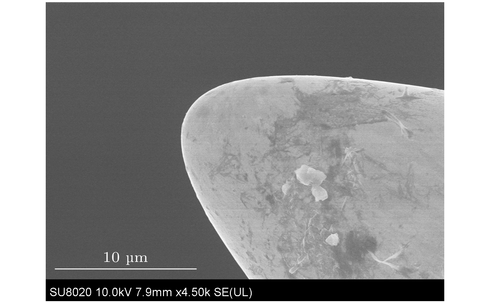
图 4 微间隙放电图像 (a) 间隙为100 μm, 放电前针板形貌; (b) 间隙为50 μm, 电压为1600 V下采集到的放电图像; (c) 间隙为100 μm, 电压为1600 V下采集到的放电图像; (d) 间隙为150 μm, 电压为1600 V下采集到的放电图像
Figure 4. The discharge photographs of micro-gap: (a) The gap is 100 μm, the shape of the needle board before discharge; (b) the discharge photograph is collected at a gap of 50 μm and a voltage of 1600 V; (c) the discharge photograph is collected at a gap of 100 μm and a voltage of 1600 V; (d) the discharge photograph is collected at a gap of 150 μm and a voltage of 1600 V.
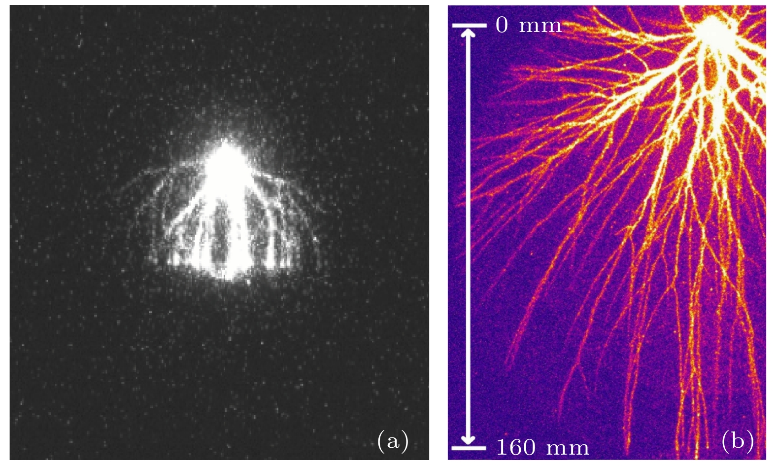
图 5 文献[23]中短间隙的放电图像 (a) 大气压下针板间距为10 mm的放电图像(pd = 1000 kPa·mm); (b) 气压为400 mbar (1 bar = 105 Pa)针板间距为160 mm的放电图像 (pd = 6400 kPa·mm)
Figure 5. Discharge photographs of micro-gap in reference [23]: (a) The discharge photograph with needle-plate spacing of 10 mm under atmospheric pressure (pd = 1000 kPa·mm); (b) the discharge photograph with air pressure of 400 mbar (1 bar =105 Pa) and needle-plate spacing of 160 mm (pd = 6400 kPa·mm).
图 6 大气压下针板间距为100 μm空气放电通道的建立过程 (a) 电源电压约为900 V时, 针尖起晕的放电图像; (b) 电源电压约为1200 V时, 电晕击穿流注的放电图像; (c) 电源电压约为1600 V时的火花放电图像
Figure 6. The process of establishing an air discharge channel with a needle plate spacing of 100 μm under atmospheric pressure: (a) The corona discharge photograph when the power supply voltage is about 900 V; (b) the corona streamer breakdown discharge photograph when the power supply voltage is about 1200 V; (c) the spark discharge photograph when the power supply voltage is about 1600 V.
图 15 概率发展指数η = 1.15—1.3时仿真的分形维数 (a) η = 1.15, D = 1.422; (b) η = 1.18, D = 1.4183; (c) η = 1.2, D = 1.4031; (d) η = 1.3, D = 1.384
Figure 15. Fractal dimension of simulation of probability development index η = 1.15–1.3: (a) η = 1.15, D = 1.422; (b) η = 1.18, D = 1.4183; (c) η = 1.2, D = 1.4031; (d) η = 1.3, D = 1.384.
表 1 空气放电的主要反应过程及反应速率常数[24]
Table 1. The main reaction process and reaction rate constant of air discharge[24].
序号 反应 反应速率常数 R1 e + N2 → e + N2 f (ε) R2 e + N2 → 2e + ${\rm{N}}_2^+ $ f (ε) R3 e + O2 → e + O2 f (ε) R4 e + O2 → 2e + ${\rm{O}}_2^+ $ f (ε) R5 e + O2 → O + O– f (ε) R6 e + ${\rm{O}}_2^+ $ → 2O 2.42×10⁻¹³ (300/Te) R7 e + ${\rm{O}}_4^+ $ → 2O2 1.4×10⁻¹² (300/Te)0.5 R8 e + 2O2 → O2+${\rm{O}}_2^- $ 2×10–41 (300/Te) R9 e + ${\rm{N}}_2^+ $ + N2 → 2N2 6.07×10⁻³⁴$T_{\rm{e}}^{-2.5}$ R10 2e + ${\rm{N}}_2^+ $ → e + N2 5.651×10⁻²⁷$T_{\rm{e}}^{-0.8}$ R11 ${\rm{N}}_2^+ $ + O2 + N2 → ${\rm{O}}_4^+ $ + O2 5×10–41 R12 ${\rm{N} }_2^+$+ N2 + N2 → ${\rm{N} }_4^+$ + N2 5×10–41 R13 ${\rm{N} }_4^+$ + O2 → ${\rm{O}}_2^+ $ + 2N2 2.5×10⁻¹⁶ R14 ${\rm{N}}_2^+ $ + O2 → ${\rm{O}}_2^+ $ + N2 1.04×10⁻¹⁵$T^{-0.5} $ R15 2N2 + ${\rm{O}}_2^+ $ → N2${\rm{O}}_2^+ $ + N2 8.1×10–38$T^{-2} $ R16 N2 + N2${\rm{O}}_2^+ $ → 2N2 + ${\rm{O}}_2^+ $ 14.6$T^{-5.3} $
exp (–2357/T)R17 O2 + N2${\rm{O}}_2^+ $ → N2 + ${\rm{O}}_4^+ $ 1×10–15 R18 ${\rm{O}}_2^+ $ + O2 + N2 → ${\rm{O}}_4^+ $ + N2 2.04×10⁻³⁴$T^{-3.2} $ R19 ${\rm{O}}_2^+ $ + O2 + O2 → ${\rm{O}}_4^+ $ + O2 2.04×10⁻³⁴$T^{-3.2} $ R20 ${\rm{O}}_4^+ $ + ${\rm{O}}_2^- $ → 3O2 1×10–13 R21 ${\rm{O}}_4^+ $+${\rm{O}}_2^- $ + O2→ 3O2 + O2 2×10–37 R22 ${\rm{O}}_4^+ $+${\rm{O}}_2^- $ + N2→ 3O2+N2 2×10–37 R23 ${\rm{O}}_2^+ $ + ${\rm{O}}_2^- $ + O2 → 3O2 2×10–37 R24 ${\rm{O}}_2^+ $+${\rm{O}}_2^- $ + N2→ 2O2+N2 2×10–37 R25 O2 + O + N2 → O3 + N2 2.5×10–46 R26 O2 + O + O2 → O3 + O2 2.5×10–46 R27 ${\rm{O}}_2^+ $ + O– → O + O2 3.46×10⁻¹²$T^{-0.5} $ 注: 反应中二体碰撞的反应速率常数单位为 m3/s; 三体碰撞的反应速率常数单位为 m6/s; Te和T 单位为 K, 其中Te为电子温度. 表 2 仿真运行10次得到的分形维数
Table 2. Fractal dimension obtained by running the simulation ten times.
仿真次数 η = 1.1 η = 1.15 η = 1.18 η = 1.2 η = 1.3 η = 1.4 1 1.4099 1.4246 1.4013 1.3808 1.3797 1.2969 2 1.4478 1.3906 1.4183 1.3877 1.3808 1.3713 3 1.4683 1.395 1.4428 1.4079 1.384 1.3106 4 1.43 1.47 1.3732 1.4399 1.3656 1.3579 5 1.4592 1.4475 1.4252 1.4031 1.4183 1.3229 6 1.4855 1.3957 1.4609 1.4006 1.3591 1.3846 7 1.4979 1.4283 1.4233 1.4344 1.4001 1.3524 8 1.4985 1.3978 1.4006 1.3764 1.4079 1.3378 9 1.4274 1.4428 1.4381 1.3696 1.4016 1.3179 10 1.4169 1.422 1.3441 1.4155 1.4006 1.3656 均值 1.4541 1.4214 1.4128 1.4016 1.3898 1.3418 95%置信区间 [1.4306 1.4777] [1.4023 1.4405] [1.3881 1.4375] [1.3846 1.4186] [1.3762 1.4034] [1.3210 1.3625] -
[1] 欧阳吉庭, 张宇, 秦宇 2016 高电压技术 42 673
 Google Scholar
Ouyang J T, Zhang Y, Qin Y 2016 High Voltage Engineering 42 673
 Google Scholar
[2] 郑殿春, 丁宁, 沈湘东, 赵大伟, 郑秋平, 魏红庆 2016 物理学报 65 024703
 Google Scholar
Zheng D C, Ding N, Shen X D, Zhao D W, Zheng Q P, Wei H Q 2016 Acta Phys. Sin. 65 024703
 Google Scholar
[3] 火元莲, 张广庶, 吕世华, 袁萍 2013 物理学报 62 059201
 Google Scholar
Huo Y L, Zhang G S, Lü S H, Yuan P 2013 Acta Phys. Sin. 62 059201
 Google Scholar
[4] 贾志东, 乐波, 蒋雄伟 1999 高电压技术 25 1
 Google Scholar
Jia Z D, Le B, Jiang X W 1999 High Voltage Engineering 25 1
 Google Scholar
[5] Niemeyer L, Pietronero L, Wiesmann H J 1984 Phys. Rev. Lett. 52 12
[6] Wiesmann H J, Zeller H R 1986 J. Phys. D: Appl. Phys. 60 1770
 Google Scholar
[7] Georghiou G E, Morrow R, Metaxas A C 2000 J. Phys. D: Appl. Phys. 33 2453
 Google Scholar
[8] Hallac A, Georghiou G E, Metaxas A C 2005 IEEE Trans. Plasma Sci. 33 266
 Google Scholar
[9] Carazzetti P, Renaud P, Shea H R 2008 Proceedings of SPIE. 6884 199
[10] 廖瑞金, 伍飞飞, 刘兴华, 杨帆, 杨丽君, 周之, 翟蕾 2012 物理学报 61 245201
 Google Scholar
Liao R J, Wu F F, Liu X H, Yang F, Yang L J, Zhou Z, Zhai L 2012 Acta Phys. Sin. 61 245201
 Google Scholar
[11] 陈伟根, 汪万平, 夏青 2013 电工技术学报 28 50
 Google Scholar
Chen W G, Wang W P, Xia Q 2013 Transaction of China Electrotechnical Society 28 50
 Google Scholar
[12] 李晗蔚, 孙安邦, 张幸, 姚聪伟, 常正实, 张冠军 2018 物理学报 67 045101
 Google Scholar
Li H W, Sun A B, Zhang X, Yao C W, Chang Z S, Zhang G J 2018 Acta Phys. Sin. 67 045101
 Google Scholar
[13] 成永红, 孟国栋, 董承业 2017 电工技术学报 32 13
Cheng Y H, Meng G D, Dong C Y 2017 Transaction of China Electrotechnical Society 32 13
[14] 孟国栋, 成永红, 酉小广, 吴锴 2012 西安交通大学学报 46 106
Meng G D, Cheng Y H, You X G, Wu K 2012 Journal of Xian Jiaotong University 46 106
[15] Slade P G, Taylor E D 2002 IEEE Trans. on Components and Packaging Technologies 25 390
 Google Scholar
[16] Torres J M, Dhariwal R S, King P C 1999 Nanotechnology 10 102
 Google Scholar
[17] Venkattraman A, Alexeenko A A 2012 Phys. Plasmas 19 103301
[18] 徐学基, 诸定昌 1996 气体放电物理 (上海: 复旦大学出版社) 第243−268页
Xu X J, Zhu D C 1996 Gas discharge physics(Shanghai: Fudan Press) pp243−268 (in Chinese)
[19] 杨津基 1983 气体放电 (北京: 科学出版社) 第105−217页
Yang J J 1983 Gas Discharge (Beijing: Science Press) p105−217 (in Chinese)
[20] 安韵竹, 文习山, 胡元潮, 王羽, 李勋, 咸日常, 李海涛, 陈佳佳 2017 中国电机工程学报 37 2734
 Google Scholar
An Y Z, Wen X S, Hu Y C, Wang Y, Li X, Xian R C, Li H T, Chen J J 2017 Proceedings of the CSEE. 37 2734
 Google Scholar
[21] Gagnepain J J, Roques-Carmes C 1986 Wear 109 119
 Google Scholar
[22] Sarkar N, Chaudhuri B B 1992 Pattern Recognit. 25 1035
 Google Scholar
[23] Briels T M P, Van Veldhuizen E M, Ebert U 2008 IEEE Trans. Plasma Sci. 36 4
 Google Scholar
[24] Liu X H, He W, Yang F, Wang H Y, Liao R J, Xiao H G 2012 Chin. Phys. B 21 075201
 Google Scholar
Catalog
Metrics
- Abstract views: 10110
- PDF Downloads: 131
- Cited By: 0


 DownLoad:
