-
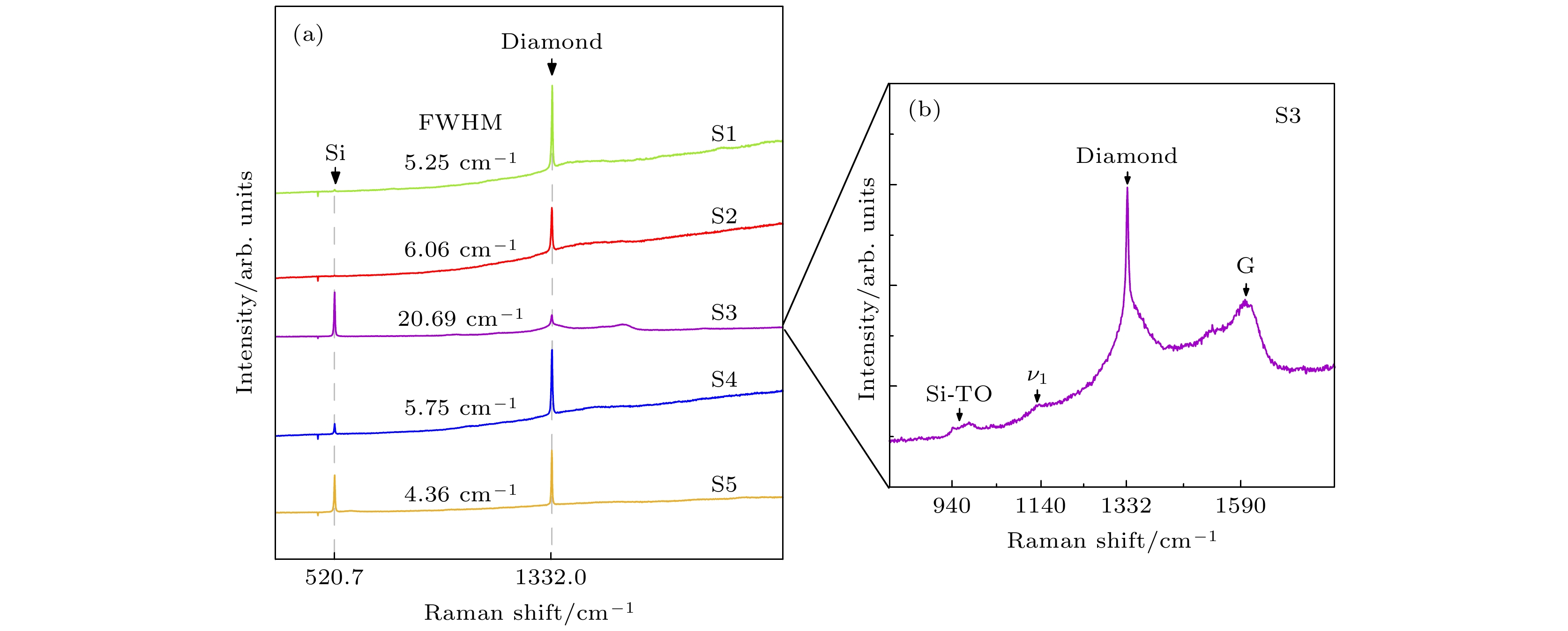
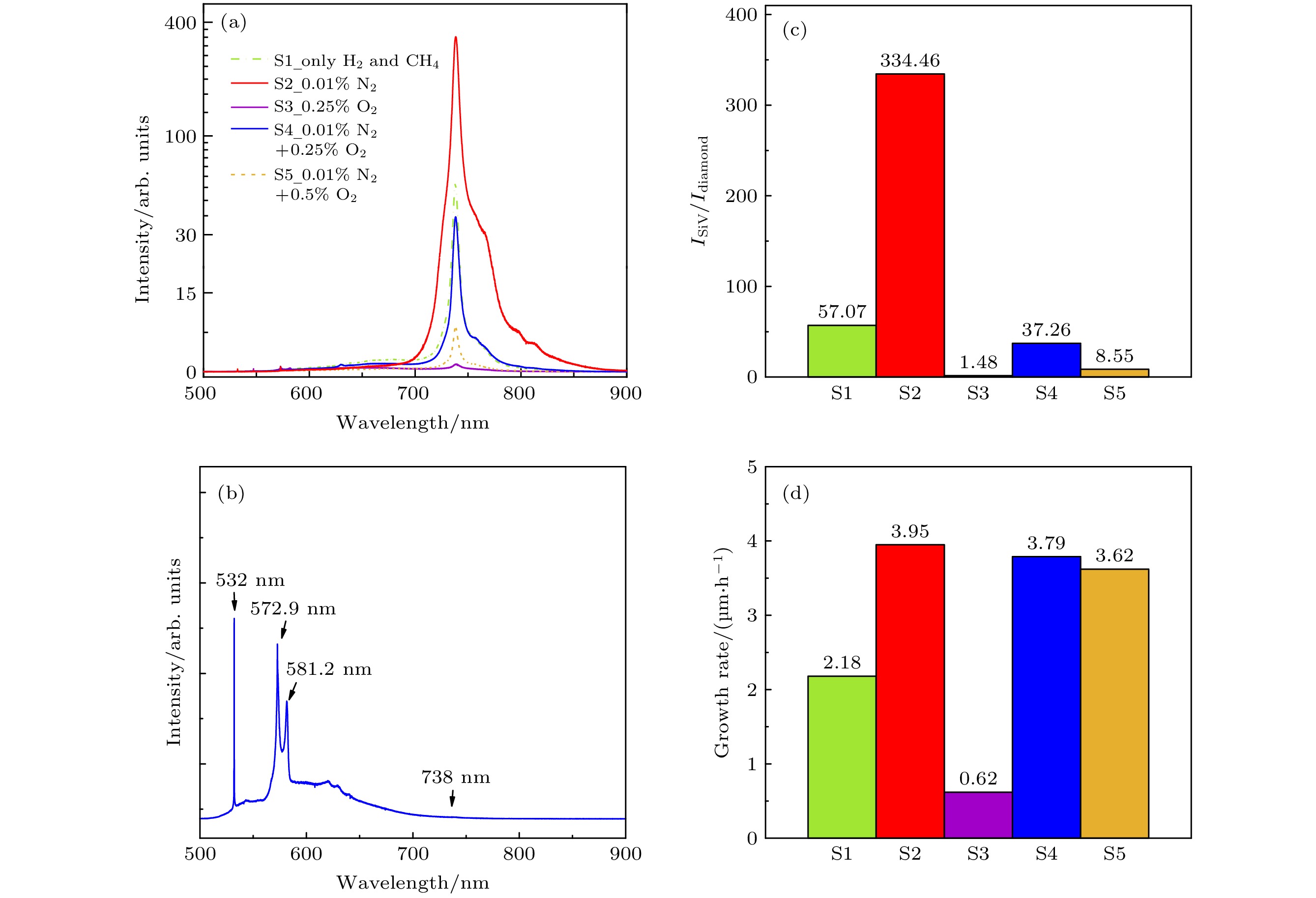
Diamond silicon vacancy centers (SiV centers) have important application prospects in quantum information technology and biomarkers. In this work, the formation mechanism and regulation method of SiV center during the growth of polycrystalline diamond on silicon substrate are studied. By changing the ratio of nitrogen content to oxygen content in the growing atmosphere of diamond, the photoluminescence intensity of SiV center can be controlled effectively, and polycrystalline diamond samples with the ratios of SiV center photoluminescence peak to diamond intrinsic peak as high as 334.46 and as low as 1.48 are prepared. It is found that nitrogen promotes the formation of SiV center in the growth process, and the inhibition of oxygen. The surface morphology and photoluminescence spectrum for each of these samples show that the photoluminescence peak intensity of SiV center is positively correlated with the grain size of diamond, and the SiV center’s photoluminescence peak in the diamond film with obvious preferred orientation of crystal plane is higher. The distribution of Si centers and SiV centers on the surface of polycrystalline diamond are further characterized and analyzed by photoluminescence, Raman surface scanning and depth scanning spectroscopy. It is found that during the growth of polycrystalline diamond, the substrate silicon diffuses first into the diamond grain and then into the crystal structure to form the SiV center. This paper provides a theoretical basis for the development and application of SiV centers in diamond.
-
Keywords:
- diamond /
- silicon vacancy center /
- photoluminescence /
- Raman spectroscopy
[1] Schrand A M, Hens S A C, Shenderova O A 2009 Crit. Rev. Solid State Mater. Sci. 34 18
 Google Scholar
[2] Yu S J, Kang M W, Chang H C, Chen M C, Yu Y C 2005 J. Am. Chem. Soc. 127 17604
 Google Scholar
[3] Pingault B, Jarausch D D, Hepp C, Klintberg L, Becker J N, Markham M, Becher C, Atatüre M 2017 Nat. Commun. 8 15579
 Google Scholar
[4] Rose B C, Huang D, Zhang Z H, Stevenson P, Tyryshkin A M, Sangtawesin S, Srinivasan S, Loudin L, Markham M L, Edmonds A M, Twitchen D J, Lyon S A, deLeon N P 2018 Science 361 60
 Google Scholar
[5] Bradac C, Gao W, Forneris J, Trusheim M E, Aharonovich I 2019 Nat. Commun. 10 5625
 Google Scholar
[6] Le Sage D, Arai K, Glenn D R, Devience S J, Pham L M, Rahn-Lee L, Lukin M D, Yacoby A, Komeil A, Walsworth R L 2013 Nature 496 486
 Google Scholar
[7] Aharonovich I, Neu E 2014 Adv. Opt. Mater. 2 911
 Google Scholar
[8] A. M. Zaitsev 2000 Phys. Rev. B 61 12909
 Google Scholar
[9] Dobrinets I A, Vins V G, Zaitsev A M 2013 HPHT-Treated Diamonds (Vol. 181) (Berlin: Springer)
[10] Ganesan K, Ajikumar P K, Ilango S, Mangamma G, Dhara S 2019 Diamond Relat. Mater. 92 150
 Google Scholar
[11] Goss J P, Jones R, Breuer S J 1996 Phys. Rev. Lett. 77 3041
 Google Scholar
[12] Rogers L J, Jahnke K D, Teraji T, Marseglia M, Müller C, Naydenov B, Schauffert H, Kranz C, Isoya J, McGuinness L P, Jelezko F 2014 Nat. Commun. 5 4739
 Google Scholar
[13] Sternschulte H, Thonke K, Sauer R 1994 Phys. Rev. B. 50 14554
 Google Scholar
[14] Feng T, Schwartz B D 1993 J. Appl. Phys. 73 1415
 Google Scholar
[15] Neu E, Steinmetz D, Riedrich-Möller J, Gsell S, Fischer M, Schreck M, Becher C 2011 New J. Phys. 13 25012
 Google Scholar
[16] Ralchenko V G, Sedov V S, Martyanov A K, Bolshakov A P, Boldyrev K N, Krivobok V S, Nikolaev S N, Bolshedvorskii S V, Rubinas O R, Akimov A V, Khomich A A, Bushuev E V, Khmelnitsky R A, Konov V I 2019 Acs Photonics 6 66
 Google Scholar
[17] Neu E, Albrecht R, Fischer M, Gsell S, Schreck M, Becher C 2012 Phys. Rev. B 85 245207
 Google Scholar
[18] Yang B, Li J, Guo L, Huang N, Liu L, Zhai Z, Long W, Jiang X 2018 CrystEngComm 20 1158
 Google Scholar
[19] Neu E K 2012 Silicon Cacancy Color Centers in Chemical Vapor Deposition Diamond: New Insights into Promising Solid State Single Photon Sources (Saarbrücken: Universität des Saarlandes)
[20] Yang B, Yu B, Li H N, Huang N, Liu L S, Jiang X 2019 Carbon 156 242
 Google Scholar
[21] Dragounová K, Ižák T, Kromka A, Potůček Z, Bryknar Z, Potocký S 2018 Appl. Phys. A 124 219
 Google Scholar
[22] Potocký S, Izsák T, Varga M, Kromka A 2015 Phys. Status Solidi B 252 2580
 Google Scholar
[23] Sedov V, Ralchenko V, Khomich A A, Vlasov I, Vul A, Savin S, Goryachev A, Konov V 2015 Diamond Relat. Mater. 56 23
 Google Scholar
[24] Lv R Y, Yang X G, Yang D W, Niu C Y, Zhao C X, Qin J X, Zang J H, Dong F Y, Dong L, Shan C X 2021 Chin. Phys. Lett. 38 076101
 Google Scholar
[25] Wan L F, Mu C Y, Liu Y F, Cheng S H, Wang Q L, Li L A, Li H D, Zou G T 2022 Chin. Phys. Lett. 39 036801
 Google Scholar
[26] 王峰浩, 胡晓君 2013 物理学报 62 158101
 Google Scholar
Wang F H, Hu X J 2013 Acta Phys. Sin. 62 158101
 Google Scholar
[27] Lagomarsino S, Flatae A M, Kambalathmana H, Sledz F, Hunold L, Soltani N, Reuschel P, Sciortino S, Gelli N, Massi M, Czelusniak C, Giuntini L, Agio M 2021 Front. Phys. 8 601362
 Google Scholar
[28] Locher R, Wild C, Herres N, Behr D, Koidl P 1994 Appl. Phys. Lett. 65 34
 Google Scholar
[29] Ferrari A C, Robertson J 2001 Phys. Rev. B 63 121405
 Google Scholar
[30] Ferrari A C, Robertson J 2000 Phys. Rev. B 61 14095
 Google Scholar
[31] Ferrari A C, Robertson J 2001 Phys. Rev. B 64 075414
 Google Scholar
[32] Wei W 2007 Vacuum 81 857
 Google Scholar
[33] Shah S I, Waite M M 1992 Appl. Phys. Lett. 61 3113
 Google Scholar
[34] Wang J J, Lv F X 1996 Chin. Phys. Lett. 13 473
 Google Scholar
-
图 1 (a) 硅衬底金刚石样品的光致发光光谱, 纵轴刻度范围0—20是线性坐标, 20—500是对数坐标; (b) 钼衬底上以样品S1生长条件生长的金刚石样品的光致发光光谱; (c) S1—S5硅空位色心荧光峰与金刚石本征峰的比值; (d) 硅衬底金刚石样品生长速率
Figure 1. (a) SiV photoluminescence spectra of diamond samples, the scale range on the vertical axis is 0–20 for linear coordinates, and 20–500 for logarithmic coordinate; (b) photoluminescence spectra of diamond samples grown on molybdenum substrate under sample S1 growth condition; (c) ratio of SiV fluorescence peak to diamond intrinsic peak of sample; (d) growth rate of samples.
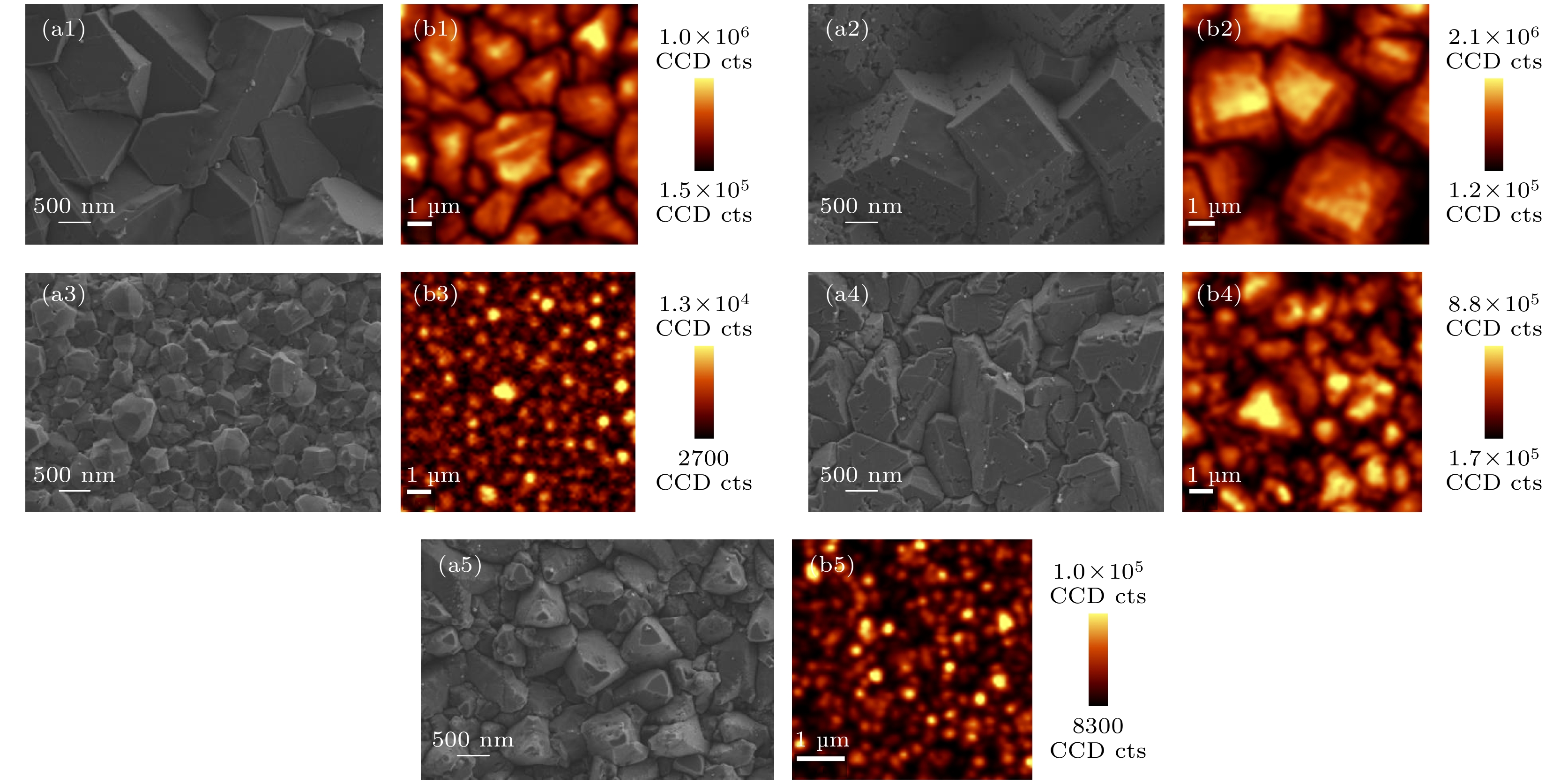
图 2 (a1)—(a5)不同生长条件的金刚石薄膜表面形貌; (b1)—(b5) 以738 nm (硅空位零声子线)为中心的PL表面扫描测试结果(测试范围10 μm× 10 μm, 测试步长100 nm), 其中(a1), (b1) S1; (a2), (b2) S2; (a3), (b3) S3; (a4), (b4) S4; (a5), (b5) S5
Figure 2. Morphology (a1)–(a5) and SiV photoluminescence mapping (b1)–(b5) of diamond film under different growth conditions, the test range of the latter is 10 μm×10 μm, and the test step is 100 nm: (a1), (b1) S1; (a2), (b2) S2; (a3), (b3) S3; (a4), (b4) S4; (a5), (b5) S5.
图 3 不同生长条件的金刚石薄膜以738 nm (硅空位零声子线)为中心的PL深度扫描测试结果(测试深度范围为聚焦深度±4 μm, 长度12 μm, 测试扫描步距为100 nm) (a) S2; (b) S5
Figure 3. SiV photoluminescence mapping in the vertical direction of diamond film under different growth conditions, the depth range of the test was ±4 μm, the length was 12 μm, and the scanning step was 100 nm: (a) S2; (b) S5.
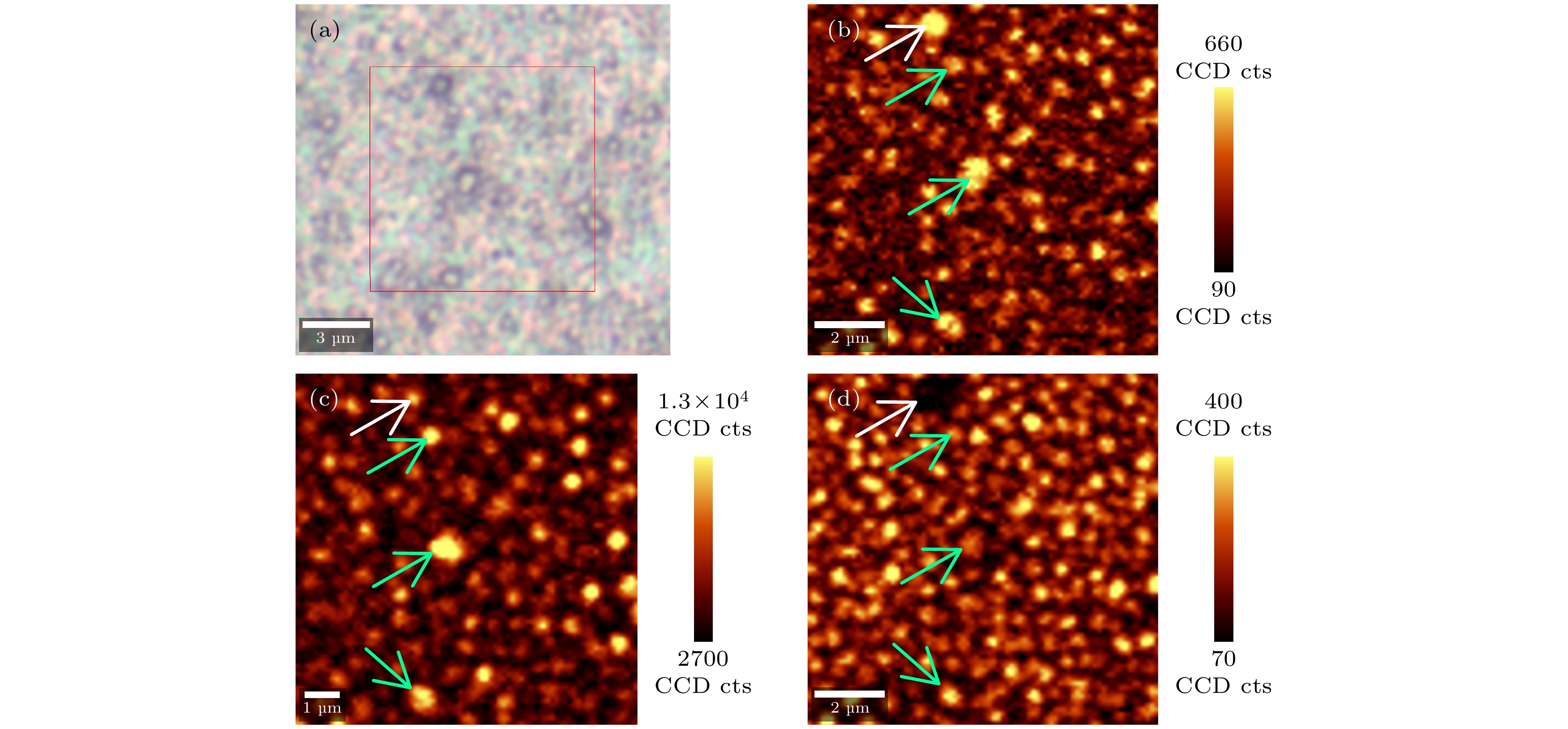
图 5 样品S3的面扫描结果 (a)样品面扫描测试区域为红框所示10 μm×10 μm区域, 测试步长为100 nm; (b)以1332 cm–1 (金刚石)为中心的拉曼面扫描结果; (c) 以738 nm (金刚石硅空位色心)为中心的PL面扫描结果; (d)以520.7 cm–1 (硅单质)为中心的拉曼面扫描结果; 箭头指出了几个晶粒在各图当中的位置, 从光谱看白色箭头所指的晶粒无硅单质信号, 绿色箭头所指的晶粒既有硅单质信号也有硅空位色心信号
Figure 5. Test zone of sample S3 mapping: (a) The scanning test area of the sample surface is the 10 μm×10 μm area shown in the red box, and the test step is 100 nm; (b) Raman mapping centered on 1332 cm–1; (c) PL mapping centered on 738 nm; (d) Raman mapping centered on 520.7 cm–1. The arrows indicate the positions of several grains in each diagram, from the spectrum, the grains indicated by the white arrows have no silicon simple substance signal, while the grains indicated by the green arrows have both silicon simple substance signal and silicon vacancy color center signal.
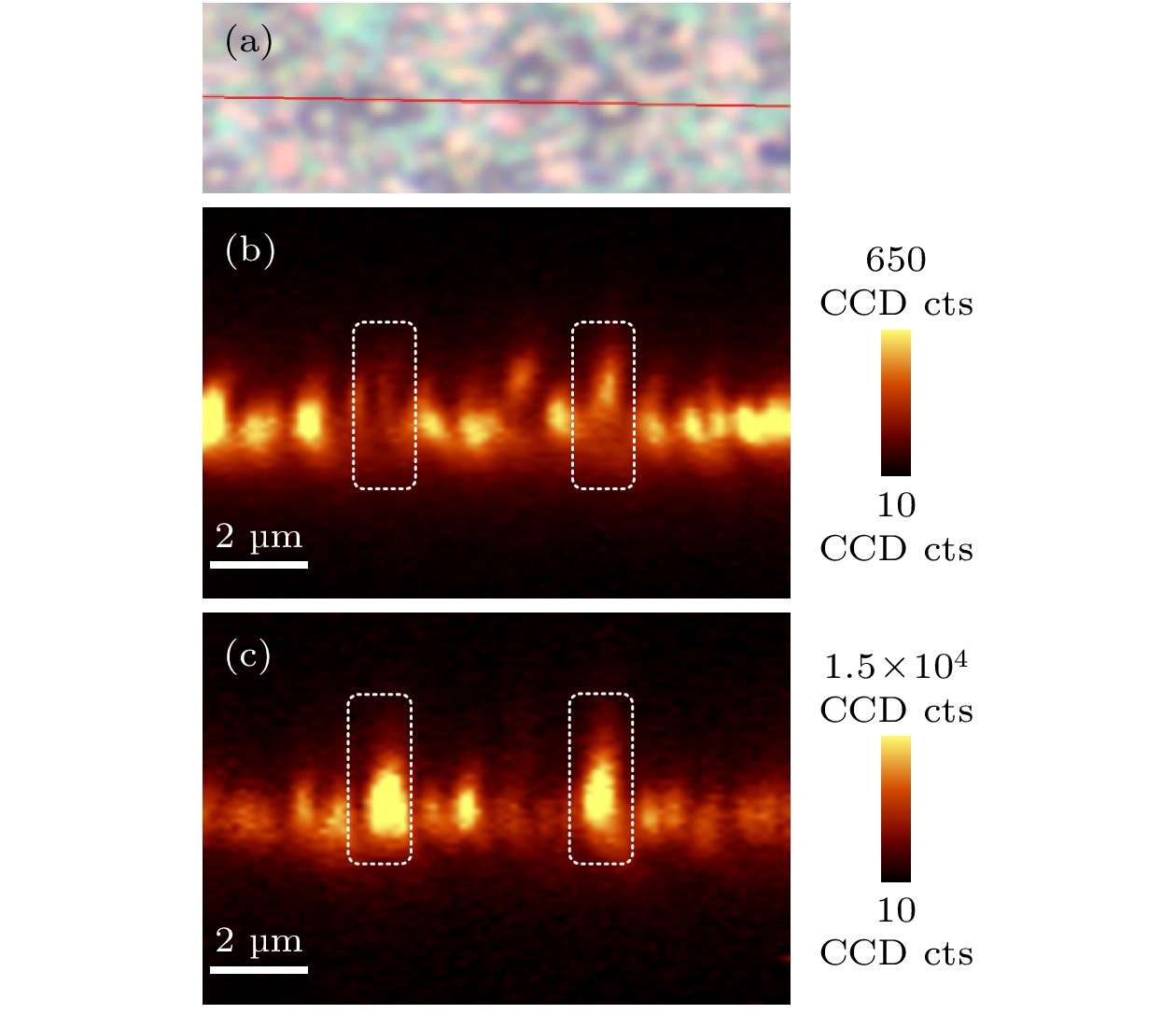
图 6 (a)样品S3做深度扫描的表面位置; (b)以520.7 cm–1(硅单质)为中心的拉曼深度扫描结果; (c)以738 nm (硅空位零声子线)为中心的PL深度扫描结果. 虚线框内的大晶粒中硅单质基本都转化为硅空位色心
Figure 6. (a) Test zone of sample S3 mapping in the vertical direction, the scanning test area of the sample surface area shown in the red line, and the test step is 100 nm; (b) Raman mapping centered on 520.7 cm–1; (c) PL mapping centered on 738 nm. Silicon elements in the large grains in the wire frame are basically transformed into silicon vacancy color centers.
表 1 样品生长工艺参数汇总(1 sccm = 1 mL/min, 1 bar = 105 Pa)
Table 1. Summary of the growth parameters.
微波功
率/W气压/
mbar总气
体流
量/sccm甲烷
流量
/sccm氮气
流量
/sccm氧气
流量
/sccmS1 4200 185 200 10 0 0 S2 4200 185 200 10 0.02 0 S3 4200 185 200 10 0 0.5 S4 4200 185 200 10 0.02 0.5 S5 4200 185 200 10 0.02 1.0 -
[1] Schrand A M, Hens S A C, Shenderova O A 2009 Crit. Rev. Solid State Mater. Sci. 34 18
 Google Scholar
[2] Yu S J, Kang M W, Chang H C, Chen M C, Yu Y C 2005 J. Am. Chem. Soc. 127 17604
 Google Scholar
[3] Pingault B, Jarausch D D, Hepp C, Klintberg L, Becker J N, Markham M, Becher C, Atatüre M 2017 Nat. Commun. 8 15579
 Google Scholar
[4] Rose B C, Huang D, Zhang Z H, Stevenson P, Tyryshkin A M, Sangtawesin S, Srinivasan S, Loudin L, Markham M L, Edmonds A M, Twitchen D J, Lyon S A, deLeon N P 2018 Science 361 60
 Google Scholar
[5] Bradac C, Gao W, Forneris J, Trusheim M E, Aharonovich I 2019 Nat. Commun. 10 5625
 Google Scholar
[6] Le Sage D, Arai K, Glenn D R, Devience S J, Pham L M, Rahn-Lee L, Lukin M D, Yacoby A, Komeil A, Walsworth R L 2013 Nature 496 486
 Google Scholar
[7] Aharonovich I, Neu E 2014 Adv. Opt. Mater. 2 911
 Google Scholar
[8] A. M. Zaitsev 2000 Phys. Rev. B 61 12909
 Google Scholar
[9] Dobrinets I A, Vins V G, Zaitsev A M 2013 HPHT-Treated Diamonds (Vol. 181) (Berlin: Springer)
[10] Ganesan K, Ajikumar P K, Ilango S, Mangamma G, Dhara S 2019 Diamond Relat. Mater. 92 150
 Google Scholar
[11] Goss J P, Jones R, Breuer S J 1996 Phys. Rev. Lett. 77 3041
 Google Scholar
[12] Rogers L J, Jahnke K D, Teraji T, Marseglia M, Müller C, Naydenov B, Schauffert H, Kranz C, Isoya J, McGuinness L P, Jelezko F 2014 Nat. Commun. 5 4739
 Google Scholar
[13] Sternschulte H, Thonke K, Sauer R 1994 Phys. Rev. B. 50 14554
 Google Scholar
[14] Feng T, Schwartz B D 1993 J. Appl. Phys. 73 1415
 Google Scholar
[15] Neu E, Steinmetz D, Riedrich-Möller J, Gsell S, Fischer M, Schreck M, Becher C 2011 New J. Phys. 13 25012
 Google Scholar
[16] Ralchenko V G, Sedov V S, Martyanov A K, Bolshakov A P, Boldyrev K N, Krivobok V S, Nikolaev S N, Bolshedvorskii S V, Rubinas O R, Akimov A V, Khomich A A, Bushuev E V, Khmelnitsky R A, Konov V I 2019 Acs Photonics 6 66
 Google Scholar
[17] Neu E, Albrecht R, Fischer M, Gsell S, Schreck M, Becher C 2012 Phys. Rev. B 85 245207
 Google Scholar
[18] Yang B, Li J, Guo L, Huang N, Liu L, Zhai Z, Long W, Jiang X 2018 CrystEngComm 20 1158
 Google Scholar
[19] Neu E K 2012 Silicon Cacancy Color Centers in Chemical Vapor Deposition Diamond: New Insights into Promising Solid State Single Photon Sources (Saarbrücken: Universität des Saarlandes)
[20] Yang B, Yu B, Li H N, Huang N, Liu L S, Jiang X 2019 Carbon 156 242
 Google Scholar
[21] Dragounová K, Ižák T, Kromka A, Potůček Z, Bryknar Z, Potocký S 2018 Appl. Phys. A 124 219
 Google Scholar
[22] Potocký S, Izsák T, Varga M, Kromka A 2015 Phys. Status Solidi B 252 2580
 Google Scholar
[23] Sedov V, Ralchenko V, Khomich A A, Vlasov I, Vul A, Savin S, Goryachev A, Konov V 2015 Diamond Relat. Mater. 56 23
 Google Scholar
[24] Lv R Y, Yang X G, Yang D W, Niu C Y, Zhao C X, Qin J X, Zang J H, Dong F Y, Dong L, Shan C X 2021 Chin. Phys. Lett. 38 076101
 Google Scholar
[25] Wan L F, Mu C Y, Liu Y F, Cheng S H, Wang Q L, Li L A, Li H D, Zou G T 2022 Chin. Phys. Lett. 39 036801
 Google Scholar
[26] 王峰浩, 胡晓君 2013 物理学报 62 158101
 Google Scholar
Wang F H, Hu X J 2013 Acta Phys. Sin. 62 158101
 Google Scholar
[27] Lagomarsino S, Flatae A M, Kambalathmana H, Sledz F, Hunold L, Soltani N, Reuschel P, Sciortino S, Gelli N, Massi M, Czelusniak C, Giuntini L, Agio M 2021 Front. Phys. 8 601362
 Google Scholar
[28] Locher R, Wild C, Herres N, Behr D, Koidl P 1994 Appl. Phys. Lett. 65 34
 Google Scholar
[29] Ferrari A C, Robertson J 2001 Phys. Rev. B 63 121405
 Google Scholar
[30] Ferrari A C, Robertson J 2000 Phys. Rev. B 61 14095
 Google Scholar
[31] Ferrari A C, Robertson J 2001 Phys. Rev. B 64 075414
 Google Scholar
[32] Wei W 2007 Vacuum 81 857
 Google Scholar
[33] Shah S I, Waite M M 1992 Appl. Phys. Lett. 61 3113
 Google Scholar
[34] Wang J J, Lv F X 1996 Chin. Phys. Lett. 13 473
 Google Scholar
Catalog
Metrics
- Abstract views: 7765
- PDF Downloads: 168
- Cited By: 0


 DownLoad:
