-
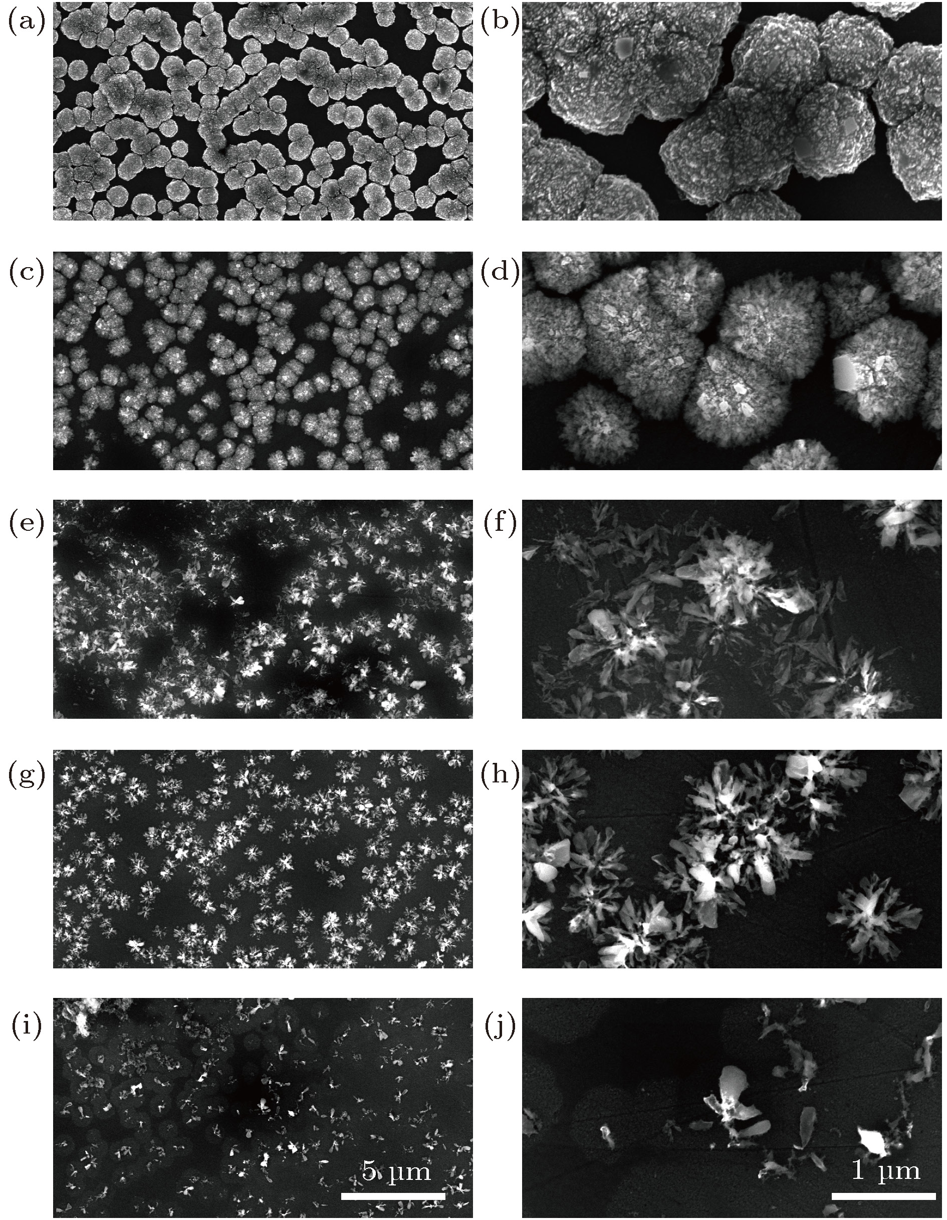
In order to increase the oxidation sites for enhancing the Si-V photoluminescence intensity of nanocrytalline diamond films, we prepare nanocrystalline diamond films; these films each are comprised of separated domains and oxidized for different times. Each single domain consists of nanodiamond grains with a size of larger than 100 nm and amorphous carbon. In the gaps between domains of separated domain there is formed a film that allows more sites to contact air to ensure the efficient oxidation of the film. As a result, silicon vacancy photoluminescence intensity of the separated domain forming the film is largely enhanced by about 22.7 times after oxidation. The SEM images and Raman spectra of oxidized samples show that the film contains flower-shaped diamond aggregates, each of which is comprised of radially arranged diamond grains. The mixture of nanodiamond grains and amorphous carbon fills the gaps between diamond petals. These fillers disappear after long-term oxidation, but the diamond petals stay stable. Raman spectra show that the amount of amorphous carbon largely decreases after oxidation, while diamond content apparently rises. Hydrogen is desorbed from the film after short-time oxidation according to Raman spectra, thus the quenching effect on silicon vacancy photoluminescence caused by hydrogen termination of diamond surface state is removed. Diamond petals of large size and nanodiamond grains in the fillers are both silicon vacancy photoluminescence sources of the film; the exposed diamond flats on the surface of unoxidized domains provide limited silicon vacancy photoluminescence for the film. The sufficient exposure of diamond grains after the removal of amorphous carbon leads to the significant enhancement of film’s silicon vacancy photoluminescence. With longer-time oxidation, the photoluminescence of film will slightly decrease due to the disappearance of small-sized nanodiamond grains, but the film photoluminescence almost remains stable in both intensity and property due to the stability of large-sized diamond grains. The film after 140-min oxidation remains photoluminescence enhancement, 8.3 times the photoluminescence of the unoxidized sample. The full width at half maximum of photoluminescence peak declines to merely 5.6-6.0 nm because of diamond petals’ high degree of order, which is advantageous for diamond silicon vacancy photoluminescence.
-
Keywords:
- diamond /
- silicon vacancy center /
- oxidation /
- photoluminescence
[1] Aharonovich I, Englund D, Toth M 2016 Nat. Photon. 10 631
 Google Scholar
[2] Aharonovich I, Castelletto S, Simpson D A, Su C H, Greentree A D, Prawer S 2011 Rep. Prog. Phys. 740 076501
[3] Aharonovich I, Neu E 2014 Adv. Opt. Mater. 2 911
 Google Scholar
[4] Schröder T, Mouradian S L, Zheng J, Trusheim M E, Walsh M, Chen E H, Li L, Bayn I, Englund D 2016 J. Opt. Soc. Am. B 33 B65
 Google Scholar
[5] Schirhagl R, Chang K, Loretz M, Degen C L 2014 Annu. Rev. Phys. Chem. 65 83
 Google Scholar
[6] Muller T, Hepp C, Pingault B, Neu E, Gsell S, Schreck M, Sternschulte H, Steinmuller-Nethl D, Becher C, Atature M 2014 Nat. Commun. 5 3328
 Google Scholar
[7] Merson T D, Castelletto S, Aharonovich I, Turbic A, Kilpatrick T J, Turnley A M 2013 Opt. Lett. 38 4170
 Google Scholar
[8] Doherty M W, Manson N B, Delaney P, Jelezko F, Wrachtrup J, Hollenberg L C L 2013 Phys. Rep. 528 1
 Google Scholar
[9] Aharonovich I 2014 Nat. Photon. 8 818
 Google Scholar
[10] Jelezko F, Wrachtrup J 2006 Phys. Status Solidi A 203 3207
 Google Scholar
[11] Rogers L J, Jahnke K D, Teraji T, Marseglia L, Muller C, Naydenov B, Schauffert H, Kranz C, Isoya J, McGuinness L P, Jelezko F 2014 Nat. Commun. 5 4739
 Google Scholar
[12] Neu E, Albrecht R, Fischer M, Gsell S, Schreck M, Becher C 2012 Phys. Rev. B 85 245207
 Google Scholar
[13] Dragounová K, Ižák T, Kromka A, Potůček Z, Bryknar Z, Potocký Š 2018 Appl. Phys. A 124 219
[14] Hu X J, Ye J S, Liu H J, Shen Y G, Chen X H, Hu H 2011 J. Appl. Phys. 109 053524
 Google Scholar
[15] Klauser F, Steinmüller-Nethl D, Kaindl R, Bertel E, Memmel N 2010 Chem. Vapor Depos. 16 127
 Google Scholar
[16] Lin S C, Yeh C J, Kurian J, Dong C L, Niu H, Leou K C, Lin I N 2014 J. Appl. Phys. 116 183701
 Google Scholar
[17] Wilson J I B, Walton J S, Beamson G 2001 J. Electron Spectrosc. Relat. Phenom. 121 183
 Google Scholar
[18] Osswald S, Yushin G, Mochalin V, Kucheyev S O, Gogotsi Y 2006 J. Am. Chem. Soc. 128 11635
 Google Scholar
[19] Pu J C, Wang S F, Sung J C 2010 J. Alloy. Compd. 489 638
 Google Scholar
[20] Huang K, Hu X, Xu H, Shen Y, Khomich A 2014 Appl. Surf. Sci. 317 11
 Google Scholar
[21] Mei Y, Fan D, Lu S, Shen Y, Hu X 2016 J. Appl. Phys. 120 225107
 Google Scholar
[22] Nimmagadda R R, Joshi A, Hsu W L 1990 J. Mater. Res. 5 2445
 Google Scholar
[23] Obraztsov A N, Kopylov P G, Chuvilin A L, Savenko N V 2009 Diamond Relat. Mater. 18 1289
 Google Scholar
[24] Zolotukhin A, Kopylov P G, Ismagilov R R, Obraztsov A N 2010 Diamond Relat. Mater. 19 1007
 Google Scholar
[25] Hei L F, Zhao Y, Wei J J, Liu J L, Li C M, Lü F X 2017 Int. J. Miner. Metall. Mater. 24 1424
 Google Scholar
[26] Mildren R P, Butler J E, Rabeau J R 2008 Opt. Express 16 18950
 Google Scholar
[27] Reilly S, Savitski V G, Liu H, Gu E, Dawson M D, Kemp A J 2015 Opt. Lett. 40 930
 Google Scholar
[28] Hu X J, Li N 2013 Chin. Phys. Lett. 30 088102
 Google Scholar
[29] Dychalska A, Fabisiak K, Paprocki K, Makowiecki J, Iskaliyeva A, Szybowicz M 2016 Mater. Des. 112 320
 Google Scholar
[30] Prawer S, Nugent K W, Jamieson D N, Orwa J O, Bursill L A, Peng J L 2000 Chem. Phys. Lett. 332 93
 Google Scholar
[31] Prawer S, Nemanich R J 2004 Philos. Trans. R. Soc. Lond. Ser. A: Math. Phys. Eng. Sci. 362 2537
 Google Scholar
[32] Ferrari A C, Robertson J 2000 Phys. Rev. B 61 14095
 Google Scholar
[33] Ferrari A C, Robertson J 2001 Phys. Rev. B 64 075414
 Google Scholar
[34] Ferrari A C, Robertson J 2001 Phys. Rev. B 63 121405
 Google Scholar
[35] Ferrari A C, Robertson J 2004 Philos. Trans. R. Soc. A: Math. Phys. Eng. Sci. 362 2477
 Google Scholar
[36] Fecher J, Wormser M, Rosiwal S M 2016 Diamond Relat. Mater. 61 41
 Google Scholar
[37] Sails S R, Gardiner D J, Bowden M, Savage J, Rodway D 1996 Diamond Relat. Mater. 5 589
 Google Scholar
-
图 1 单颗粒层纳米晶金刚石薄膜的表面形貌 (a) OX-0; (b) OX-0; (c) OX-30; (d) OX-30; (e) OX-40; (f) OX-40; (g) OX-130; (h) OX-130; (i) OX-140; (j) OX-140
Figure 1. Morphology of separated domains formed nanocrystalline diamond film: (a) OX-0; (b) OX-0; (c) OX-30; (d) OX-30; (e) OX-40; (f) OX-40; (g) OX-130; (h) OX-130; (i) OX-140; (j) OX-140.
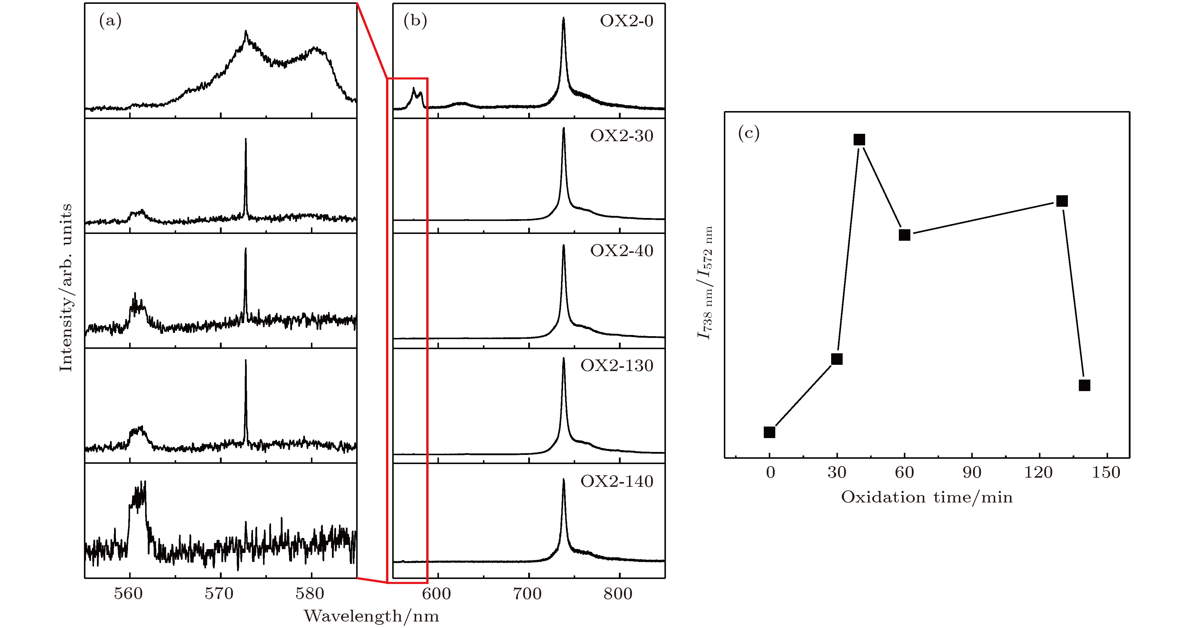
图 2 (a) 572 nm处的金刚石的一阶斯托克斯线; (b)单颗粒层纳米晶金刚石薄膜的硅空位光致发光谱; (c) 738 nm波长强度与572 nm强度比值随时间变化
Figure 2. (a) Diamond first Stokes line at 572 nm; (b) SiV photoluminescence spectra of separated domains formed nanocrystalline diamond film; (c) photoluminescence intensity ratio of 738 nm emission and 572 nm emission with different oxidation time.
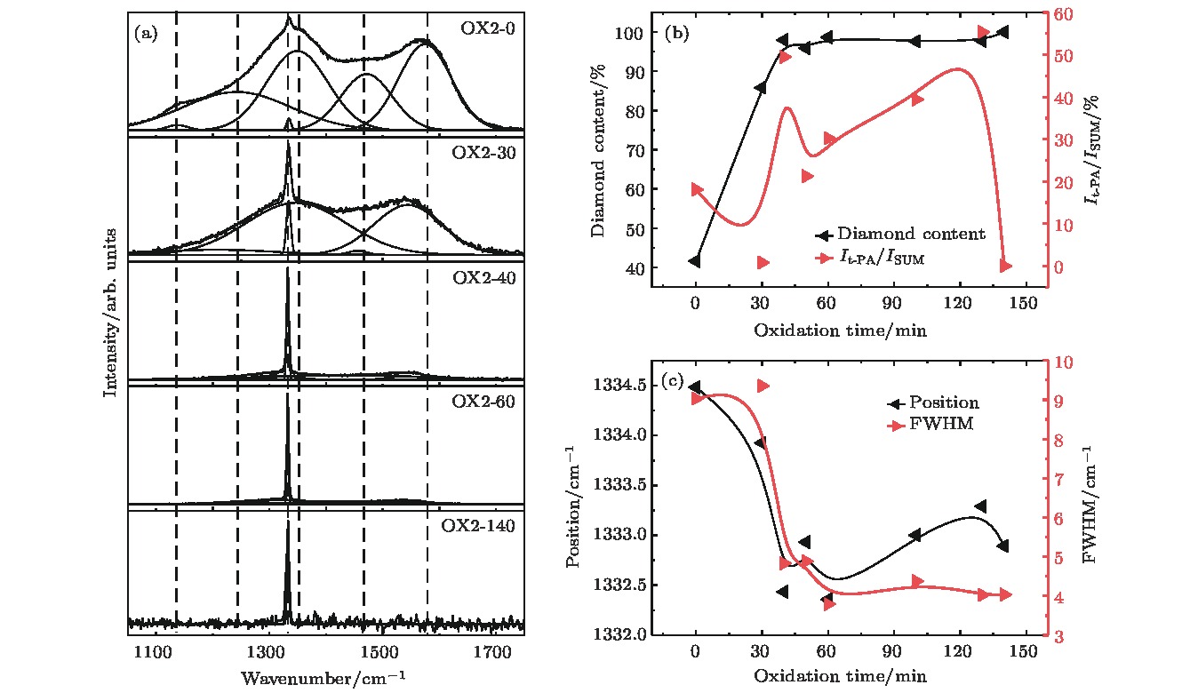
图 5 (a)不同氧化时间单颗粒层纳米晶金刚石薄膜的拉曼光谱; (b)金刚石含量与It-PA/ISUM和样品氧化时间的关系; (c)金刚石峰位置与半峰宽随氧化时间的变化关系
Figure 5. (a) Raman spectra of variety time oxidized separated domains formed nanocrystalline diamond film; (b) diamond content and It-PA/ISUM of films with their oxidation time; (c) diamond peak position and FWHM values of films with their oxidation time.
-
[1] Aharonovich I, Englund D, Toth M 2016 Nat. Photon. 10 631
 Google Scholar
[2] Aharonovich I, Castelletto S, Simpson D A, Su C H, Greentree A D, Prawer S 2011 Rep. Prog. Phys. 740 076501
[3] Aharonovich I, Neu E 2014 Adv. Opt. Mater. 2 911
 Google Scholar
[4] Schröder T, Mouradian S L, Zheng J, Trusheim M E, Walsh M, Chen E H, Li L, Bayn I, Englund D 2016 J. Opt. Soc. Am. B 33 B65
 Google Scholar
[5] Schirhagl R, Chang K, Loretz M, Degen C L 2014 Annu. Rev. Phys. Chem. 65 83
 Google Scholar
[6] Muller T, Hepp C, Pingault B, Neu E, Gsell S, Schreck M, Sternschulte H, Steinmuller-Nethl D, Becher C, Atature M 2014 Nat. Commun. 5 3328
 Google Scholar
[7] Merson T D, Castelletto S, Aharonovich I, Turbic A, Kilpatrick T J, Turnley A M 2013 Opt. Lett. 38 4170
 Google Scholar
[8] Doherty M W, Manson N B, Delaney P, Jelezko F, Wrachtrup J, Hollenberg L C L 2013 Phys. Rep. 528 1
 Google Scholar
[9] Aharonovich I 2014 Nat. Photon. 8 818
 Google Scholar
[10] Jelezko F, Wrachtrup J 2006 Phys. Status Solidi A 203 3207
 Google Scholar
[11] Rogers L J, Jahnke K D, Teraji T, Marseglia L, Muller C, Naydenov B, Schauffert H, Kranz C, Isoya J, McGuinness L P, Jelezko F 2014 Nat. Commun. 5 4739
 Google Scholar
[12] Neu E, Albrecht R, Fischer M, Gsell S, Schreck M, Becher C 2012 Phys. Rev. B 85 245207
 Google Scholar
[13] Dragounová K, Ižák T, Kromka A, Potůček Z, Bryknar Z, Potocký Š 2018 Appl. Phys. A 124 219
[14] Hu X J, Ye J S, Liu H J, Shen Y G, Chen X H, Hu H 2011 J. Appl. Phys. 109 053524
 Google Scholar
[15] Klauser F, Steinmüller-Nethl D, Kaindl R, Bertel E, Memmel N 2010 Chem. Vapor Depos. 16 127
 Google Scholar
[16] Lin S C, Yeh C J, Kurian J, Dong C L, Niu H, Leou K C, Lin I N 2014 J. Appl. Phys. 116 183701
 Google Scholar
[17] Wilson J I B, Walton J S, Beamson G 2001 J. Electron Spectrosc. Relat. Phenom. 121 183
 Google Scholar
[18] Osswald S, Yushin G, Mochalin V, Kucheyev S O, Gogotsi Y 2006 J. Am. Chem. Soc. 128 11635
 Google Scholar
[19] Pu J C, Wang S F, Sung J C 2010 J. Alloy. Compd. 489 638
 Google Scholar
[20] Huang K, Hu X, Xu H, Shen Y, Khomich A 2014 Appl. Surf. Sci. 317 11
 Google Scholar
[21] Mei Y, Fan D, Lu S, Shen Y, Hu X 2016 J. Appl. Phys. 120 225107
 Google Scholar
[22] Nimmagadda R R, Joshi A, Hsu W L 1990 J. Mater. Res. 5 2445
 Google Scholar
[23] Obraztsov A N, Kopylov P G, Chuvilin A L, Savenko N V 2009 Diamond Relat. Mater. 18 1289
 Google Scholar
[24] Zolotukhin A, Kopylov P G, Ismagilov R R, Obraztsov A N 2010 Diamond Relat. Mater. 19 1007
 Google Scholar
[25] Hei L F, Zhao Y, Wei J J, Liu J L, Li C M, Lü F X 2017 Int. J. Miner. Metall. Mater. 24 1424
 Google Scholar
[26] Mildren R P, Butler J E, Rabeau J R 2008 Opt. Express 16 18950
 Google Scholar
[27] Reilly S, Savitski V G, Liu H, Gu E, Dawson M D, Kemp A J 2015 Opt. Lett. 40 930
 Google Scholar
[28] Hu X J, Li N 2013 Chin. Phys. Lett. 30 088102
 Google Scholar
[29] Dychalska A, Fabisiak K, Paprocki K, Makowiecki J, Iskaliyeva A, Szybowicz M 2016 Mater. Des. 112 320
 Google Scholar
[30] Prawer S, Nugent K W, Jamieson D N, Orwa J O, Bursill L A, Peng J L 2000 Chem. Phys. Lett. 332 93
 Google Scholar
[31] Prawer S, Nemanich R J 2004 Philos. Trans. R. Soc. Lond. Ser. A: Math. Phys. Eng. Sci. 362 2537
 Google Scholar
[32] Ferrari A C, Robertson J 2000 Phys. Rev. B 61 14095
 Google Scholar
[33] Ferrari A C, Robertson J 2001 Phys. Rev. B 64 075414
 Google Scholar
[34] Ferrari A C, Robertson J 2001 Phys. Rev. B 63 121405
 Google Scholar
[35] Ferrari A C, Robertson J 2004 Philos. Trans. R. Soc. A: Math. Phys. Eng. Sci. 362 2477
 Google Scholar
[36] Fecher J, Wormser M, Rosiwal S M 2016 Diamond Relat. Mater. 61 41
 Google Scholar
[37] Sails S R, Gardiner D J, Bowden M, Savage J, Rodway D 1996 Diamond Relat. Mater. 5 589
 Google Scholar
Catalog
Metrics
- Abstract views: 12971
- PDF Downloads: 69
- Cited By: 0


 DownLoad:
