


In commemoration of the 100th anniversary of the birth of Kun Huang
编者按:
2019 年是世界著名物理学家、中国固体和半导体物理学奠基人之一, 黄昆先生诞辰100 周年. 黄昆先生不仅在固体物理领域取得了卓越的成就, 而且更重要的是,他花费了大量的精力为我国培养了大批半导体科技人才. 1956 年3 月, 我国集中了全国600 多位科学家,制定了12 年科学技术发展规划, 提出了“发展计算技术、半导体技术、无线电电子学、自动学和远距离操纵技术的紧急措施方案”. 同年暑假, 我国创办了第一个五校联合半导体专业, 黄昆先生任半导体教研室主任, 谢希德先生任副主任, 从此开启了我国自主培养半导体科技人才的新纪元. 经过了60 多年的发展, 我国半导体学科, 包括半导体材料、物理和器件等方面都取得了巨大的进步. 为纪念黄昆先生, 2019 年9 月1—3 日, 中国科学院半导体研究所、北京大学、中国物理学会和九三学社在北京西郊宾馆联合举办“纪念黄昆先生诞辰100 周年暨半导体学科发展研讨会”, 本刊特邀请部分与会专家撰写了半导体材料、物理和器件等领域的研究论文和综述文章, 组成专题. 本专题包括1 篇研究论文和10 篇综述文章, 分别来自中国科学院上海微系统研究所、长春光机所、半导体研究所、物理研究所和浙江大学、电子科技大学、南昌大学、东北师范大学、香港大学等单位的科研团队, 介绍了国内外半导体学科相关领域的最新进展和发展方向, 希望本专题的出版可以为我国半导体学科的学术交流和发展做一些贡献, 并以此来纪念黄昆先生百年诞辰.
2019, 68 (16): 168504.
doi: 10.7498/aps.68.20191262
Abstract +
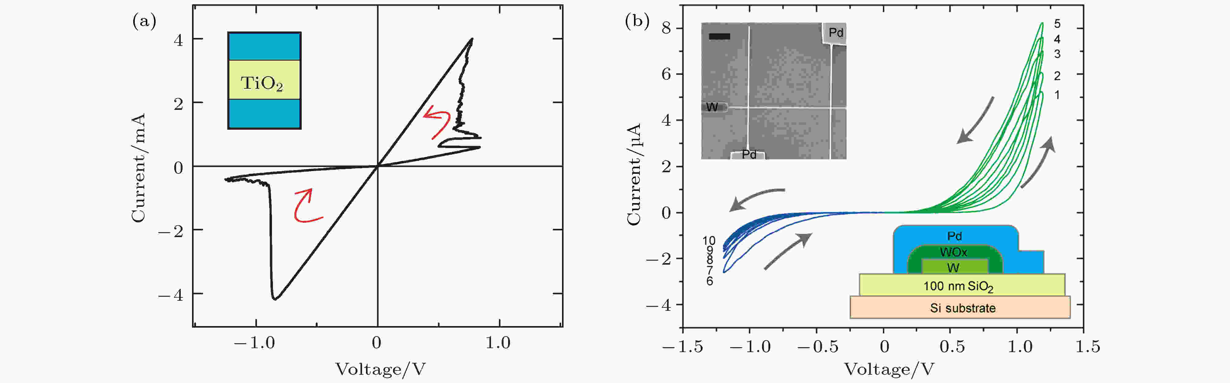
Memristors are considered to be the potential candidate for simulating synapses due to their high density, low power consumption and continuously adjustable resistance. Metal oxide is an ideal choice for fabricating memristive devices with high performance due to its advantages of oxygen migration, easy adjustment of components and compatibility with traditional CMOS. In this review paper, the memristive behaviors and operation mechanism of oxide-based memristors including digital-type memristors and analog-type memristors are first introduced. We mainly summarize the cognitive functions simulated by analog-type memristive synapse, including nonlinear-transmission characteristic, synaptic plasticity, learning experience, and non-associative/associative learning. Then, the potential applications of memristive synapse in pattern recognition, sound localization, logic operation, flexibility/transferability and optoelectronic memristive synapse are introduced. Finally, we provide an outlook of the future possible studies of oxide-based memristive synapse in the relevant fields.


2019, 68 (16): 168503.
doi: 10.7498/aps.68.20191044
Abstract +
The development of semiconductor light-emitting diode (LED) in the visible emission range is very unbalance, as the power efficiency of yellow LED is far below other colors. Based on the GaN/Si technology, the authors and his team made a systematic research from the aspect of material growth, chip fabrication, device physics and equipment design, resolved the problems of epi-film cracking, high dislocation density, large strain in quantum well (QW), phase separation in QW, low QW growth temperature, low hole concentration, light absorption by substrate and light blocking by electrode, successfully made a breakthrough in fabricating efficient yellow LED. The yellow LED chip achieves a power efficiency of 26.7% at 20 A/cm2 with 565 nm wavelength and efficacy of 164 lm/W, and the power efficiency goes up to 42.8% at 1 A/cm2 with 577 nm wavelength and efficacy of 248 lm/W. New LED light source with multi-colors and without phosphor was developed based on the efficient yellow LEDs, opened up a new direction of pure LED healthy lighting.
2019, 68 (16): 163201.
doi: 10.7498/aps.68.20191002
Abstract +
Polarized photodetection technology has good application value in the fields of remote sensing imaging, environmental monitoring, medical detection and military equipment. Polarized photodetectors based on low-dimensional materials can use the natural anisotropy of materials to detect polarized information. Some two-dimensional materials have strong in-plane anisotropy due to their low-symmetrical crystal structure, such as black-phosphorus, black-arsenic, ReS2, GaTe, GeSe, GeAs, and TiS3. These anisotropic two-dimensional materials are appropriate for the working medium of polarized photodetectors. Numerous researchs focused on polarized photodetectors with different materials and device structures and our works are introduced. Polarized photodetectors based on such low-dimensional materials have realized a broadband photodetection, including ultraviolet, visible, and infrared lights.
2019, 68 (16): 166301.
doi: 10.7498/aps.68.20191073
Abstract +
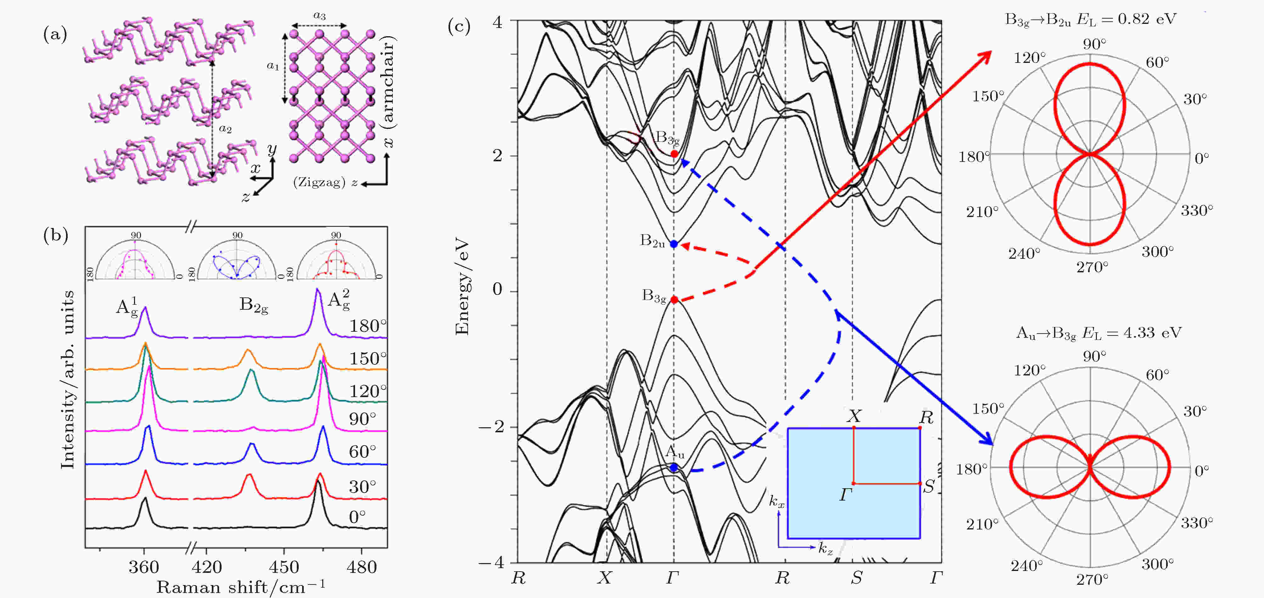
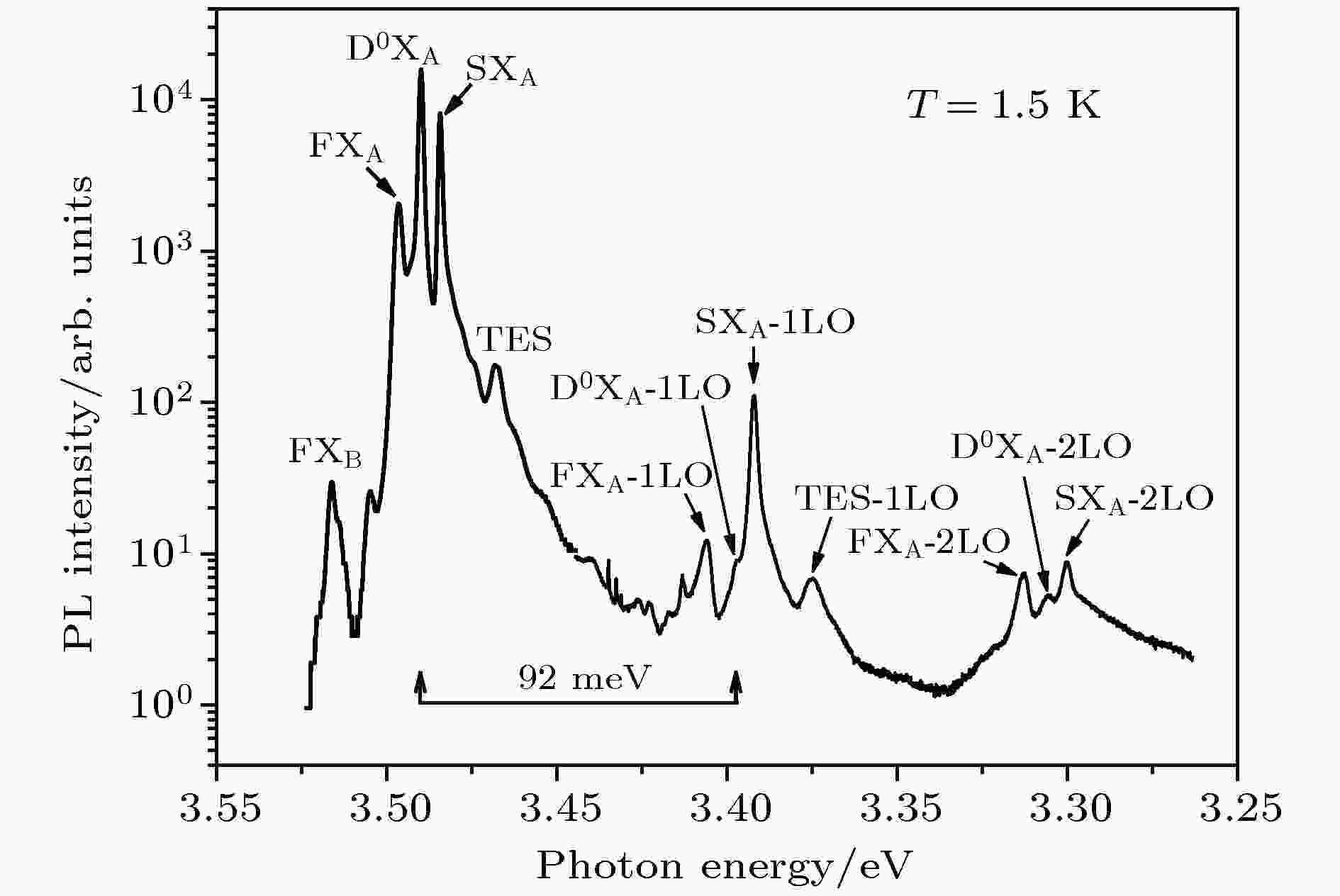
Huang and Rhys published a quantum theoretical treatment to the light absorption in F-centre in solids, which has been widely recognized as the first detailed quantum-mechanical calculation. In the Huang-Rhys’s seminal theoretical treatment, they derived a dimensionless factor to characterize electron-phonon coupling strength which was named later as Huang-Rhys factor. Since then, Huang-Rhys factor has been generally accepted. In this short review, the physical nature of Huang-Rhys factor and several application examples in solids are introduced and presented in memory of the hundredth anniversary of Prof. Kun Huang. Due to limited publication space and my personal understanding on Huang-Rhys factor, only several cases including GaN, 2D WS2 monolayer semiconductor, inorganic CsPbBr3 perovskite nanosheets and NV centers in diamond, in which the extremely-weak and medium strong coupling between electron (exciton) and phonon occur, are discussed in this short review.

2019, 68 (16): 166801.
doi: 10.7498/aps.68.20191074
Abstract +
Semiconductor heterojunctions play a crucial role in exploring novel physics and developing advanced devices. Due to the characteristic electronic band structure, such as the narrow bandgap and the large spin-orbital interaction, the Ⅳ-Ⅵ compound semiconductor heterojunctions are not only of great importance to infrared detectors, but also arouse extensively concern in the frontier fields of physics, like topological insulators (TIs) and spintronics. Most excitingly, the two-dimensional electron gas (2DGE) with high electron density and high mobility is revealed at the interface of the typical Ⅳ-Ⅵ compound semiconductor CdTe/PbTe heterojunction, the formation of which is attributed to the unique twisted interface of the Ⅳ-Ⅵ compound semiconductor heterojunctions. Further researches demonstrate that the 2DEG system boasts prominent infrared photoresponse and is of Dirac fermion nature. This review presents the major progress in Ⅳ-Ⅵ compound semiconductor heterojunction 2DEG in the past decades. First, the formation mechanism of the twisted heterojunction 2DEG is discussed based on both theoretical and experimental results. By molecular beam epitaxy the novel lattice-mismatch heterostructure CdTe/PbTe with sharp interface was obtained and first-principle calculations revealed that the alternately changed atomic layer spacing played a crucial role in the formation of 2DEG. High resolution transmission electron microscope image of the interface clearly demonstrated the twisted interfacial structure and showed that the interfacial Te-sharing bonding configuration provided the excessive electrons. Second, we show the transport properties of the 2DEG under the condition of low temperature and high magnetic field, and the unambiguous π Berry phase of quantum oscillations indicate that the 2DEG is of Dirac fermion nature and demonstrate its potential for realizing two-dimensional TI and spintronic device. Moreover, the 2DEG exhibits quite high mobility, making it candidate for high electron mobility transistor. At last, the high-performance mid-infrared photodetector is displayed, which is built based on the typical Ⅳ-Ⅵ compound semiconductor CdTe/PbTe heterojunction. The most exciting feature of the detector is that it is able to achieve high-speed response with satisfying detectivity while working at room temperature, which could be a complementation to state-of-art mid-infrared photodetectors. In summary, the Ⅳ-Ⅵ compound semiconductor heterojunctions are of great significance not only in fundamental physics but also in device applications, and this review could provide the researchers with the main results in the field.
2019, 68 (16): 167101.
doi: 10.7498/aps.68.20191239
Abstract +
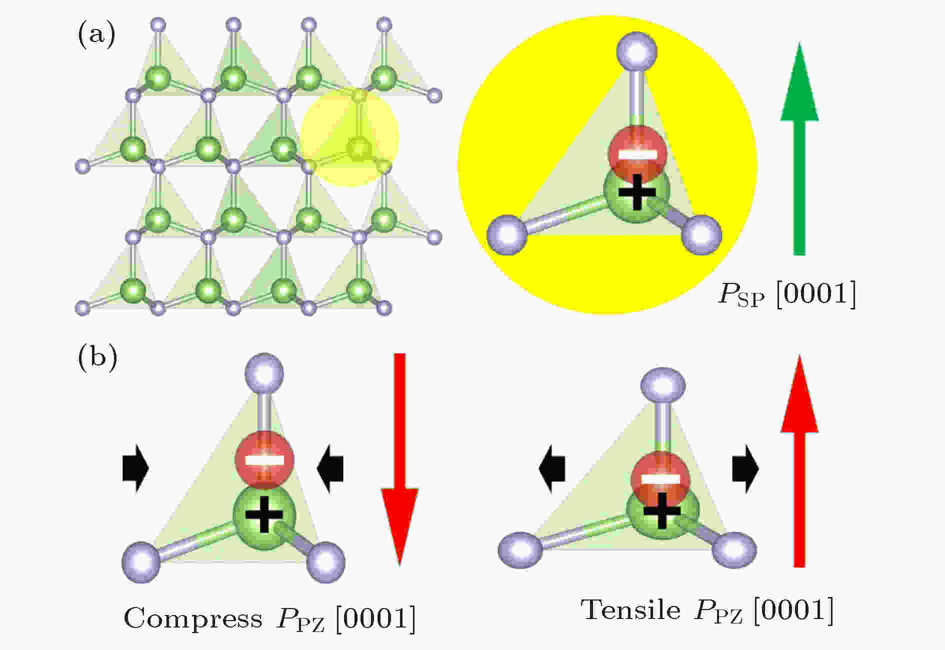
The manipulation of electronic structures of conventional semiconductors remains the key issue of modern semiconductor physics and devices. Compare to limited modulation of semiconductors by conventional gate technique, we theoretically demonstrate that, polarized interfaces can generate a strong built-in electric field (about 10 MV/cm) in both polar and non-polar semiconductors, and the polarized interfaces can tune the band gaps in a wide range (approximately 0—2 eV), and significantly enhances the Rashba spin-orbit coupling strength as well. In this paper, we introduce polarized interfaces in polar semiconductor InN and non-polar semiconductor Ge, and generate topological insulator phases by polarized interfaces. The polarized interface is compatible with conventional semiconductor fabrication techniques and shows interesting physics and potential optoelectronic applications.

Progress of the study on carrier scattering mechanisms of silicon/germanium field effect transistors
2019, 68 (16): 167301.
doi: 10.7498/aps.68.20191146
Abstract +
As the feature size of Metal-Oxide-Semiconductor Field Effect Transistors (MOSFETs) continues to decrease, large numbers of new problems appear. Techniques such as strain project, new channel materials and new device structures are considered by academics and industry to be effective ways to continue to improve device performance. In this paper, the scattering mechanism of carriers in the device channel is studied from three aspects: strain technique, new channel material and new structure device: (1) strain technique: Biaxial tensile strain can change carrier distribution among different energy levels, which affects Coulomb scattering and Coulomb mobility. Furthermore, from the TEM image, it is found that biaxial tensile reduces the channel surface roughness for Si nMOSFET, leading an enhancement of electron mobility. However, no such similar phenomena were observed in pMOSFET. Based on this, a new method for calculating the mobility of MOSFET surface roughness scattering using TEM image has been proposed. (2) New channel material: In the germanium (Ge) transistors with different crystal faces, the scattering mechanisms of electron under high field conditions are different. The phonon scattering dominates the Ge(100) transistor, while the surface roughness scattering dominates the Ge(110), (111) transistors. This result is quite different from Si MOSFET. Therefore, a unified model for the scattering mechanism of electron in Ge nMOSFET has been proposed. In SiGe transistors, alloy scattering mainly play a role in the region with relatively small effective electric field (Eeff). The strength of alloy scattering would be weakened in high field and could be decreased by reducing the thickness of SiGe layer. (3) New structure devices: In ultra-thin body germanium (GeOI) transistors, carrier transport is influenced by high- k /channel interfaces, as well as Ge channel/buried oxide (BOX) interface. As the Ge layer thickness decreases, carrier distribution is closer to the interfaces, which intensifies Coulomb scattering and surface roughness scattering. As a result, the mobility in GeOI transistor decreases as the thickness scaling. In addition, the distribution of electron in different energy valleys changes with the thickness decrease in Ge layer, which affects the scattering of electrons. When the Ge film is lower than 10 nm, a part of electron in the L valley will move to the Γ valley, causing the decrease of electron effective mass and increasing the electron mobility.

2019, 68 (16): 167502.
doi: 10.7498/aps.68.20191114
Abstract +
Due to the potential applications for spintronics devices, diluted ferromagnetic semiconductors (DMS) have received extensive attention for decades. However, in classical Ⅲ–Ⅴ based DMS material, such as (Ga,Mn)As, heterovalent (Ga3+, Mn2+) doping results in lack of individual control of carrier and spin doping, and seriously limited chemical solubility. The two difficulties prevent furtherincrease of the Curie temperature of the Ⅲ–Ⅴ based DMS. To overcome these difficulties, a series of new types of DMS with independent spin and charge doping have been synthesized, such as Ⅰ–Ⅱ–Ⅴ based LiZnAs and Ⅱ–Ⅱ–Ⅴ based (Ba,K)(Zn,Mn)2As2. In these new materials, isovalent (Zn,Mn) substitution is only spin doping, while charge is independently doped by heterovalentsubstitution of non-magnetic elements. As a result (Ba,K)(Zn,Mn)2As2 obtains the reliable record of Curie temperature (230 K) among DMS in which ferromagnetic ordering is mediated by itinerate carriers. In this review, we summarize the recent development of the new DMS materials with following aspects: 1) the discovery and synthesis of several typical new DMS materials; 2) physical properties studies with muon spin relaxation and in-situ high pressure techniques; 3) single crystal growth, Andreev reflection junction based on single crystal and measurements of spin polarization.

2019, 68 (16): 167802.
doi: 10.7498/aps.68.20191043
Abstract +
II-oxides wide-bandgap semiconductor, including the beryllium oxide (BeO), magnesium oxide (MgO), zinc oxide (ZnO), have large exciton binding energy (ZnO 60 meV, MgO 80 meV), high optical gain (ZnO 300 cm–1) and wide tunable band gap (3.37 eV ZnO, MgO 7.8 eV, BeO 10.6 eV), which are the advantages of achieving low-threshold laser devices in the ultraviolet wavelength. It is also one of the important candidates to replace the traditional gas arc lamp (such as mercury lamp, deuterium lamp, excimer lamp, xenon lamp etc.) as the source of deep ultraviolet and even vacuum ultraviolet. Although, during the past decades, the ZnO-based pn homojunction devices have made great progress in the near-UV electroluminescence, but as the band gap broadens, the acceptor (or donor) ionization energy becomes higher (On the order of hundreds meV), which causing the room temperature equivalent thermal energy (26 meV) cannot make the impurities ionizing effectively. In addition, the self-compensation effect in the doping process further weakens the carrier yield. These above drawbacks have become the bottleneck that hinders II-oxides wide-bandgap semiconductor from achieving ultraviolet laser devices and expanding to shorter wavelengths, and are also a common problem faced by other wide-bandgap semiconductor materials. The regulation of the electrical and luminescent properties of materials often depends on the control of critical defect states. The rich point defects and their combination types make the II-oxides wide-bandgap semiconductors an important platform for studying defect physics. For the identification and characterization of specific point defects, it is expected to discover and further construct shallower defect states, which will provide a basis for the regulation of electrical performance. In this paper, recent research results of II-oxides wide-bandgap semiconductors will be described from three aspects: high-quality epitaxial growth, impurity and point defects, p-type doping and ultraviolet electroluminescence. Through the overview of related research works, II-oxides wide-bandgap semiconductors are clarified as deep ultraviolet light sources materials. Meanwhile, indicates that the key to the regulation of electrical performance in the future lies in the regulation of point defects.

2019, 68 (16): 167803.
doi: 10.7498/aps.68.20191004
Abstract +
Photonic interconnects have potentials to break increasingly severe energy efficiency and bandwidth density bottlenecks of electrical interconnect in scaled complementary metal oxide semiconductor (CMOS) integrated circuits, leading to the emergence of optoelectronic integrated circuits (OEICs) that utilize electronic and photonic devices together in a synergistic way to achieve better performance than those based on pure electronic device technology. By reviewing the progresses of Si-based light-emitting device, the schematic of MOS-like light source integrated with waveguides and the following photodetector is analyzed for its availability. It is believed that on-chip optical interconnects could be achieved by standard CMOS technology successfully with the speed as fast as the velocity of light, supplying propulsions for nest-generation OEICs.

2019, 68 (16): 168102.
doi: 10.7498/aps.68.20191036
Abstract +
Graphene, as a typical representative of the two-dimensional material family, has received a wide attention due to its excellent physical and chemical properties. Graphene nanoribbon (GNR) is graphene in a width of several to a few tens of nanometers. GNRs not only inherit most of the excellent properties of graphene, but also have their own specific properties such as band gap opening and spin-polarized edge states, which make it the potential candidate in graphene based electronics in the future. Hexagonal boron nitride (h-BN), which has similar lattice constant with graphene, normally serves as an ideal substrate for graphene and GNRs. It can not only effectively preserve their intrinsic properties, but also benefit for the fabrication of electrical devices via popular semiconductor processes. In this paper, we reviewed the development history of research of graphene and GNRs on h-BN in recent years. The recent progress of physical properties is also discussed. In order to realize the large scale production of graphene and GNRs on h-BN, high quality h-BN multilayer is necessary. In addition, recent progresses about h-BN preparation methods are presented, and the progresses could pave the way for the further application of GNRs in the electronics. Finally, the research direction of graphene and GNRs on h-BN in the future is discussed.
