-
Semiconductor heterojunctions play a crucial role in exploring novel physics and developing advanced devices. Due to the characteristic electronic band structure, such as the narrow bandgap and the large spin-orbital interaction, the Ⅳ-Ⅵ compound semiconductor heterojunctions are not only of great importance to infrared detectors, but also arouse extensively concern in the frontier fields of physics, like topological insulators (TIs) and spintronics. Most excitingly, the two-dimensional electron gas (2DGE) with high electron density and high mobility is revealed at the interface of the typical Ⅳ-Ⅵ compound semiconductor CdTe/PbTe heterojunction, the formation of which is attributed to the unique twisted interface of the Ⅳ-Ⅵ compound semiconductor heterojunctions. Further researches demonstrate that the 2DEG system boasts prominent infrared photoresponse and is of Dirac fermion nature. This review presents the major progress in Ⅳ-Ⅵ compound semiconductor heterojunction 2DEG in the past decades. First, the formation mechanism of the twisted heterojunction 2DEG is discussed based on both theoretical and experimental results. By molecular beam epitaxy the novel lattice-mismatch heterostructure CdTe/PbTe with sharp interface was obtained and first-principle calculations revealed that the alternately changed atomic layer spacing played a crucial role in the formation of 2DEG. High resolution transmission electron microscope image of the interface clearly demonstrated the twisted interfacial structure and showed that the interfacial Te-sharing bonding configuration provided the excessive electrons. Second, we show the transport properties of the 2DEG under the condition of low temperature and high magnetic field, and the unambiguous π Berry phase of quantum oscillations indicate that the 2DEG is of Dirac fermion nature and demonstrate its potential for realizing two-dimensional TI and spintronic device. Moreover, the 2DEG exhibits quite high mobility, making it candidate for high electron mobility transistor. At last, the high-performance mid-infrared photodetector is displayed, which is built based on the typical Ⅳ-Ⅵ compound semiconductor CdTe/PbTe heterojunction. The most exciting feature of the detector is that it is able to achieve high-speed response with satisfying detectivity while working at room temperature, which could be a complementation to state-of-art mid-infrared photodetectors. In summary, the Ⅳ-Ⅵ compound semiconductor heterojunctions are of great significance not only in fundamental physics but also in device applications, and this review could provide the researchers with the main results in the field.
-
Keywords:
- Ⅳ-Ⅵ compound semiconductor heterojunctions /
- two-dimensional electron gas /
- Dirac fermions /
- infrared detectors
[1] Bardeen J, Brattain W H 1948 Phys. Rev. 74 230
 Google Scholar
[2] Brattain W H, Bardeen J 1948 Phys. Rev. 74 231
 Google Scholar
[3] Nakamura S, Mukai T, Senoh M 1994 Appl. Phys. Lett. 64 1687
 Google Scholar
[4] Klitzing K V, Dorda G, Pepper M 1980 Phys. Rev. Lett. 45 494
 Google Scholar
[5] König M, Wiedmann S, Brüne C, Roth A, Buhmann H, Molenkamp L W, Qi X L, Zhang S C 2007 Science 318 766
 Google Scholar
[6] Cao Y, Fatemi V, Fang S, Watanabe K, Taniguchi T, Kaxiras E, Jarillo-Herrero P 2018 Nature 556 43
 Google Scholar
[7] Rogalski A 2012 Opto-Electronics Review 20 279
[8] Springholz G, Ueta A Y, Frank N, Bauer G 1996 Appl. Phys. Lett. 69 2822
 Google Scholar
[9] Yuan S, Springholz G, Bauer G, Kriechbaum M 1994 Phys. Rev. B 49 5476
 Google Scholar
[10] Rahim M, Arnold M, Felder F, Behfar K, Zogg H 2007 Appl. Phys. Lett. 91 151102
 Google Scholar
[11] Koga T, Harman T C, Cronin S B, Dresselhaus M S 1999 Phys. Rev. B 60 14286
 Google Scholar
[12] Casian A, Sur I, Scherrer H, Dashevsky Z 2000 Phys. Rev. B 61 15965
 Google Scholar
[13] Koike K, Honden T, Makabe I, Yan F P, Yano M 2003 J. Cryst. Growth 257 212
 Google Scholar
[14] Heiss W, Groiss H, Kaufmann E, Hesser G, Böberl M, Springholz G, Schäffler F, Koike K, Harada H, Yano M 2006 Appl. Phys. Lett. 88 192109
 Google Scholar
[15] Hasegawa M M, de Andrada e Silva E A 2003 Phys. Rev. B 68 205309
 Google Scholar
[16] Si J, Jin S, Zhang H, Zhu P, Qiu D, Wu H 2008 Appl. Phys. Lett. 93 202101
 Google Scholar
[17] Cai C, Jin S, Wu H, Zhang B, Hu L, McCann P J 2012 Appl. Phys. Lett. 100 182104
 Google Scholar
[18] Jin S, Cai C, Bi G, Zhang B, Wu H, Zhang Y 2013 Phys. Rev. B 87 235315
 Google Scholar
[19] Jin S, Cai C, Zhang B, Wu H, Bi G, Si J, Zhang Y 2012 New J. Phys. 14 113021
 Google Scholar
[20] Zhang B, Cai C, Zhu H, Wu F, Ye Z, Chen Y, Li R, Kong W, Wu H 2014 Appl. Phys. Lett. 104 161601
 Google Scholar
[21] Zhang B, Lu P, Liu H, Jiao L, Ye Z, Jaime M, Balakirev F F, Yuan H, Wu H, Pan W, Zhang Y 2015 Nano Lett. 15 4381
 Google Scholar
[22] Zhang L, Shu T, Wu H, Ye Z, Zhu L 2019 Phys. Status Solidi 13 1800551
 Google Scholar
[23] Mascarenhas A 2012 Spontaneous Ordering in Semiconductor Alloys (Springer Science & Business Media)
[24] Suzuki K, Seto S, Sawada T, Imai K 2002 IEEE Trans. Nucl. Sci. 49 1287
 Google Scholar
[25] Waghmare U V, Spaldin N A, Kandpal H C, Seshadri R 2003 Phys. Rev. B 67 125111
 Google Scholar
[26] Božin E S, Malliakas C D, Souvatzis P, Proffen T, Spaldin N A, Kanatzidis M G, Billinge S J L 2010 Science 330 1660
 Google Scholar
[27] Su C H 2008 J. Appl. Phys. 103 084903
 Google Scholar
[28] Segall B, Lorenz M R, Halsted R E 1963 Phys. Rev. 129 2471
 Google Scholar
[29] Bissert G, Hesse K F 1978 Acta Crystallographica Section B 34 1322
 Google Scholar
[30] van de Walle C G, Martin R M 1987 Phys. Rev. B 35 8154
 Google Scholar
[31] Hiyamizu S, Mimura T, Fujii T, Nanbu K, Hashimoto H 1981 Jpn. J. Appl. Phys. 20 L245
 Google Scholar
[32] Ismail K, Meyerson B S, Wang P J 1991 Appl. Phys. Lett. 58 2117
 Google Scholar
[33] Kikkawa J M, Smorchkova I P, Samarth N, Awschalom D D 1997 Science 277 1284
 Google Scholar
[34] Madelung O 2012 Semiconductors: Data Handbook (Springer Science & Business Media)
[35] Ando Y 2013 J. Phys. Soc. Jpn. 82 102001
 Google Scholar
[36] Hsieh T H, Lin H, Liu J, Duan W, Bansil A, Fu L 2012 Nat. Commun. 3 982
 Google Scholar
[37] Ma S, Guo C, Xiao C, Wu F, Smidman M, Lu Y, Yuan H, Wu H 2018 Adv. Funct. Mater. 28 1803188
 Google Scholar
[38] Miao M S, Yan Q, van de Walle C G, Lou W K, Li L L, Chang K 2012 Phys. Rev. Lett. 109 186803
 Google Scholar
[39] Ueno K, Shimotani H, Yuan H, Ye J, Kawasaki M, Iwasa Y 2014 J. Phys. Soc. Jpn. 83 032001
 Google Scholar
[40] Lei B, Wang N Z, Shang C, Meng F B, Ma L K, Luo X G, Wu T, Sun Z, Wang Y, Jiang Z, Mao B H, Liu Z, Yu Y J, Zhang Y B, Chen X H 2017 Phys. Rev. B 95 020503
 Google Scholar
[41] Amirtharaj P M, Pollak F H 1984 Appl. Phys. Lett. 45 789
 Google Scholar
[42] Tian Z, Garg J, Esfarjani K, Shiga T, Shiomi J, Chen G 2012 Phys. Rev. B 85 184303
 Google Scholar
[43] Venkatasubramanian R, Siivola E, Colpitts T, O'Quinn B 2001 Nature 413 597
 Google Scholar
[44] Pei Y, LaLonde A D, Heinz N A, Snyder G J 2012 Adv. Energy Mater. 2 670
 Google Scholar
-
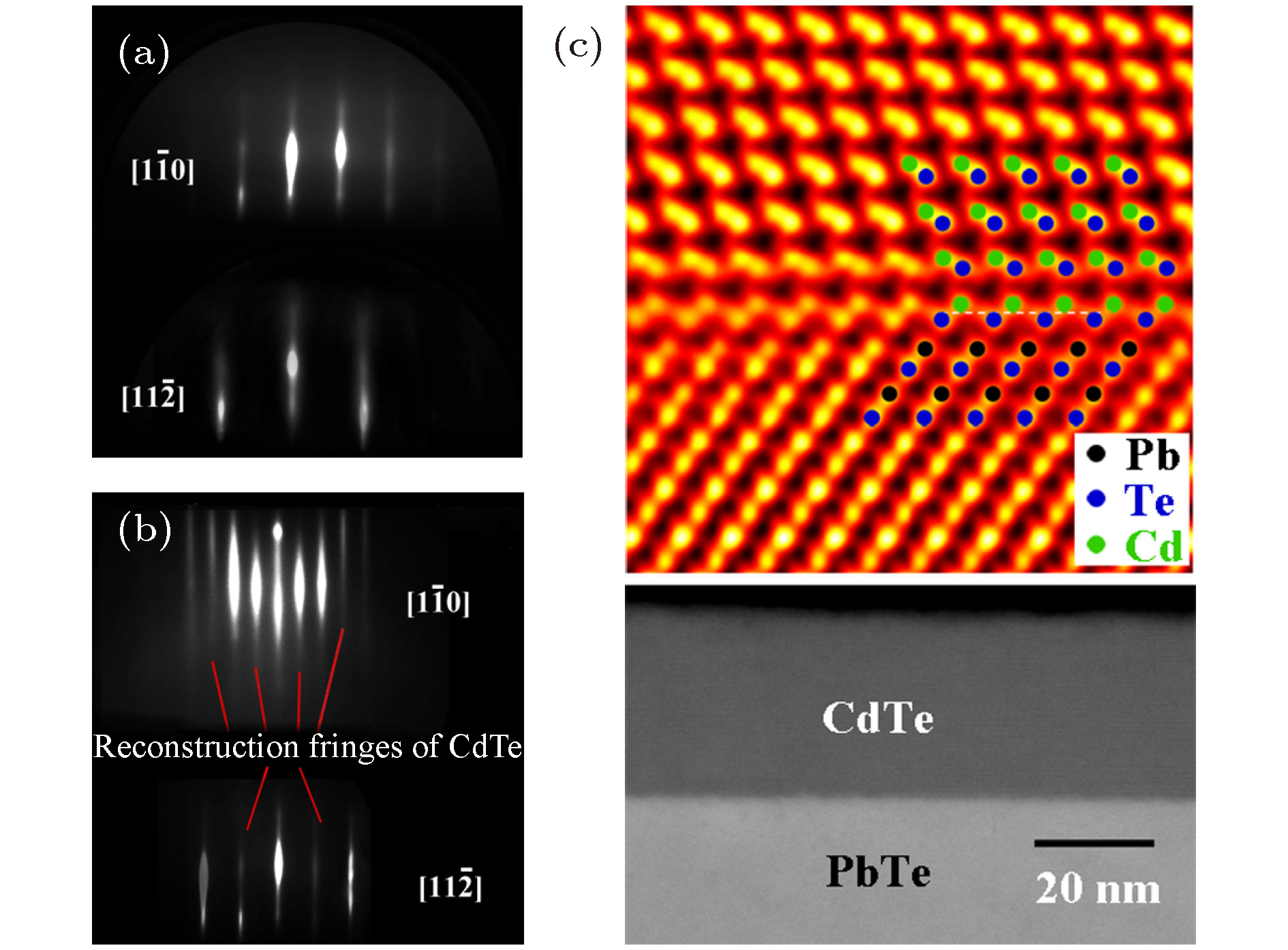
图 1 (a)生长在BaF2(111)衬底上的PbTe薄膜表面的RHEED衍射图样; (b)在PbTe薄膜表面继续生长的CdTe外延层的RHEED图样, 图中标注的方向为电子束掠入射的方向; (c) CdTe/PbTe异质结界面的相差矫正扫描透射电子显微镜图像, 清晰地反映了界面附近的原子排布, 下方的内插图是CdTe/PbTe异质结低倍透射电镜图像[19,21]
Figure 1. The RHEED patterns of (a) PbTe film grown on BaF2(111) substrate and (b) CdTe capping layer grown on the PbTe film surface; (c) aberration-corrected scanning transmission electron microscope (AC-STEM) image of the CdTe/PbTe heterojunction, showing the arrangement of atoms near the interface. The inset below is the low-magnification TEM image of the heterojunction[19,21].
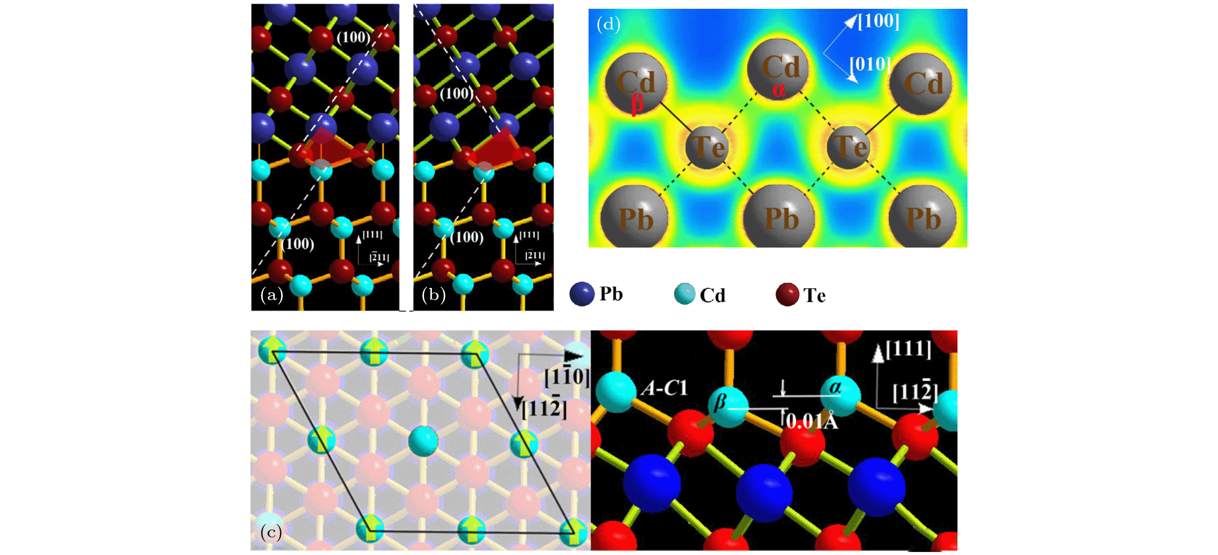
图 2 (a)内嵌于CdTe基底的PbTe量子点体系中的CdTe/PbTe(111)非扭转界面结构, 注意两层晶体各晶面是平行的, 如白色虚线标示出的(100)晶面; (b)通过在PbTe(111)表面外延CdTe得到的扭转界面结构, 注意两层晶体的(100)晶面有一个夹角, 如白色虚线所示; (c) Cd原子层开始在PbTe表面生长时的重构示意图, 左图为俯视视角, 右图为侧视视角; (d) CdTe/PbTe(111)界面的电子密度分布, 虚线表示类离子键, 实线表示类共价键[19]
Figure 2. The CdTe/PbTe(111) interface structure of (a) PbTe quantum dots embedded in CdTe and (b) CdTe layer capping on the PbTe(111) surface, it should be noted that the former is non-twisted and the latter is twisted, which is indicated by the relative position of the (100) plane of CdTe and PbTe as marked by the white dashed line; (c) the resconstruction of the first Cd layer on the PbTe(111) surface, the left panel is top-view and the right panel is side-view; (d) the electron density distributions at the twisted CdTe/PbTe(111) interface, the ionic-like and covalent-like bonds are indicated by the dashed and solid lines respectively[19].
图 3 (a)扭转界面附近的PbTe(111)晶面间距, 红色球代表Te, 深蓝色球代表Pb, 浅蓝色球代表Cd; (b)离界面30个原子层外的PbTe中的电子局域函数; (c)界面附近的PbTe中的电子局域函数; (d) Pb 6s态, (e) Pb 6p态和(f) Te 5p态的轨道分辨态密度, 蓝色线代表PbTe体材料, 黑色线和红色线分别代表未弛豫和弛豫的CdTe/PbTe(111)界面附近的PbTe层[18]
Figure 3. (a) The inter planar spacings of the PbTe(111) layers at the twisted interface; the electron localized function of PbTe (b) 30 atomic layers away from the interface and (c) at the interface; the orbital-resolved density of states of the (d) Pb 6s states, (e) 6p states, and (f) the Te 5p states for bulk PbTe (blue lines), and the PbTe layers at the twisted interface before (black lines) and after (red lines) relaxation[18].
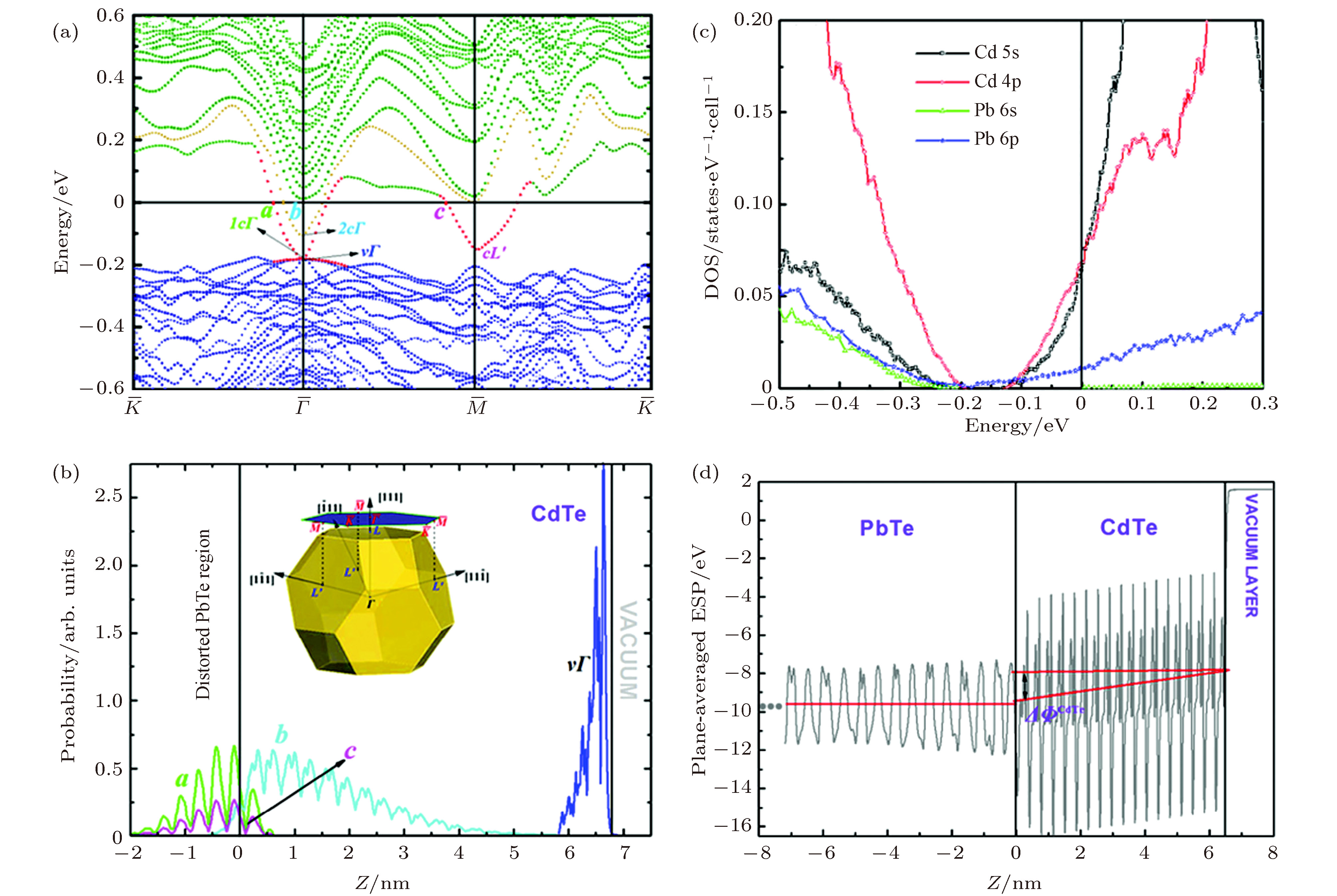
图 4 (a) PbTe(111)上CdTe薄膜的能带结构; (b)在(a)中标出的a, b, c和υΓ各态面平均波函数平方, 插图为二维布里渊区和三维布里渊区的对应关系; (c) Cd和Pb在CdTe/PbTe(111)界面处s, p的态密度; (d) CdTe/PbTe(111)界面处的面平均电势[18]
Figure 4. (a) The band structure of the nanoscale CdTe film on the PbTe (111) surface; (b) the plane-averaged wave function squares of the a, b, c, and υΓ states labeled in (a), the inset is the 2D BZ; (c) the DOS of the Cd and Pb valence s and p states at the interface of the CdTe/PbTe (111); (d) the plane-averaged ESP for the interface A formed with a 6.7 nm CdTe film on the PbTe (111) substrate[18].
图 5 (a)不同厚度CdTe覆盖层的CdTe/PbTe(111)异质结中测得的电子浓度, 内插图为通过薛定谔-泊松方程自洽求解得到的带边形状和电子面密度分布; (b) 2 —150 K CdTe/PbTe(111)异质结2DEG的电子浓度和迁移率[18]
Figure 5. (a) The electron concentrations in the CdTe/ PbTe(111) heterojunction with different CdTe capping thickness measured at 300 K, the inset shows the band profile and the electron density of the CdTe/PbTe heterojunction calculated by a Shchrodinger-Poissin solver; (b) the electron concentrations and mobilities in the CdTe/PbTe heterojunction at different temperatures[18].
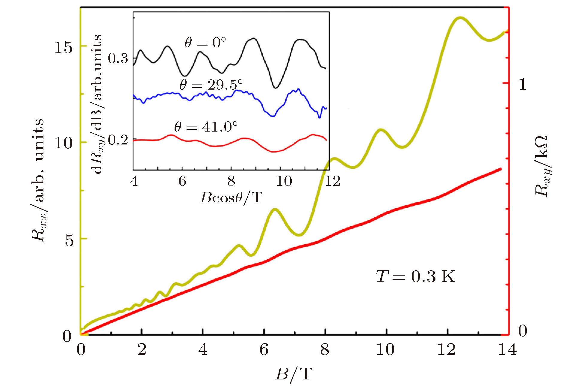
图 6 CdTe/PbTe(111)异质结的磁阻Rxx和霍尔电阻Rxy, 其中内插图为变磁场角度的dRxy/dB[21]
Figure 6. Magneto-resistance Rxx and Hall resistance Rxy in CdTe/PbTe(111) heterojunction. Quantum oscillations are observed at high magnetic fields. Plateau-like features are observed in Rxy at high B fields, where Rxx displays a strong minimum. Inset: dRxy/dB versus Bcosθ at three selected tilting angles of the magnetic field[21].
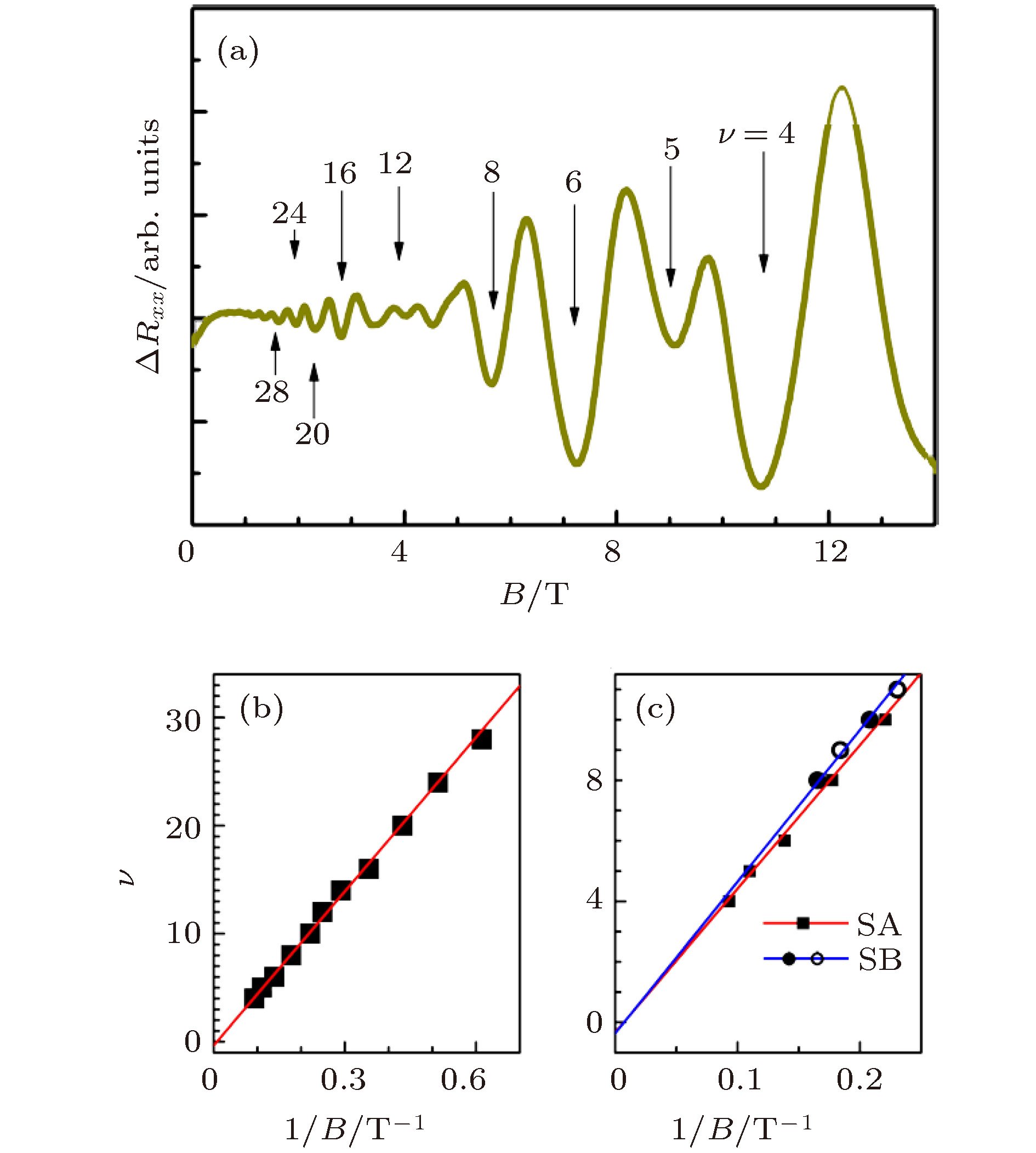
图 7 (a)扣除线性背景后的磁阻振荡部分ΔRxx, 箭头标示填充的朗道能级; (b)朗道能级线性拟合, 在1/B = 0处截距为–0.34, 接近–0.5; (c)图(b)中1/B = 0附近的局部放大图, 同时加入了在另外的样品上重复实验得到的数据(SB), 两组数据均表明, 1/B = 0处的截距接近–0.5[21]
Figure 7. (a) ΔRxx (obtained after subtracting a smooth background from Rxx) as a function of magnetic field, the arrows mark the Landau level fillings; (b) Landau level fan diagram, the line is a linear fit to the data points, the intercept at 1/B = 0 is –0.34, close to –0.5; (c) the zoomed region close to 1/B = 0 for sample A (SA), data from sample B (SB) are also included, in both samples, the intercept at 1/B = 0 is close to –0.5[21].
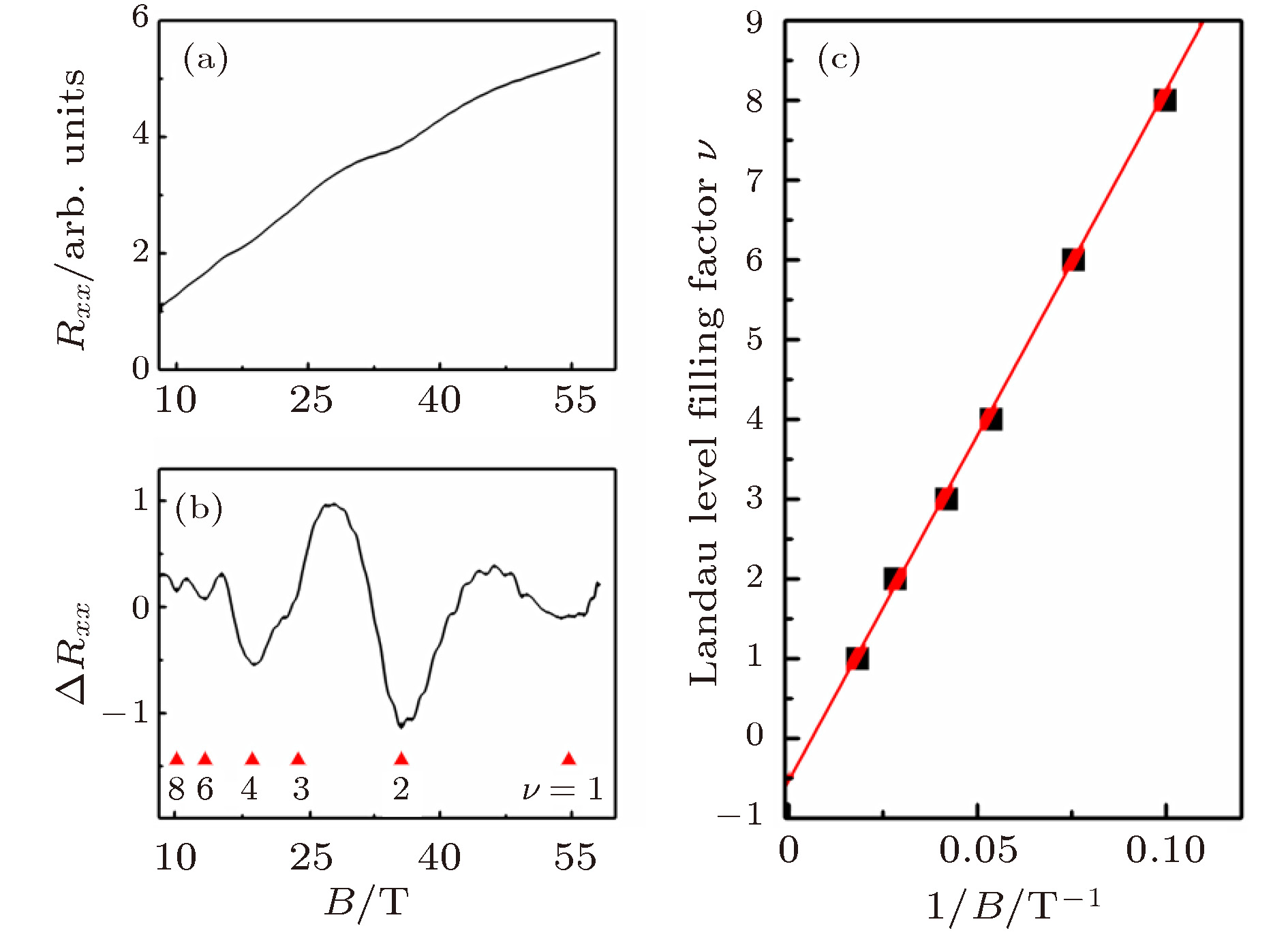
图 8 (a) CdTe/PbTe(111)异质结的磁阻Rxx; (b)扣除背景后的磁阻振荡部分ΔRxx和填充因子ν; (c)朗道能级线性拟合, 可以确切地看到1/B = 0处截距为–0.52 ± 0.07; 测量在温度1.5 K, 磁场最高达60 T的条件下进行[21]
Figure 8. (a) Rxx measured at ~ 1.5 K, quantum oscillations are clearly seen; (b) after subtracting background, the oscillating part ΔRxx is presented with the Landau filling factors marked by the red triangles; (c) Landau fan diagram linear fitting demonstrates that the intercept at 1/B = 0 is –0.52 ± 0.07[21].
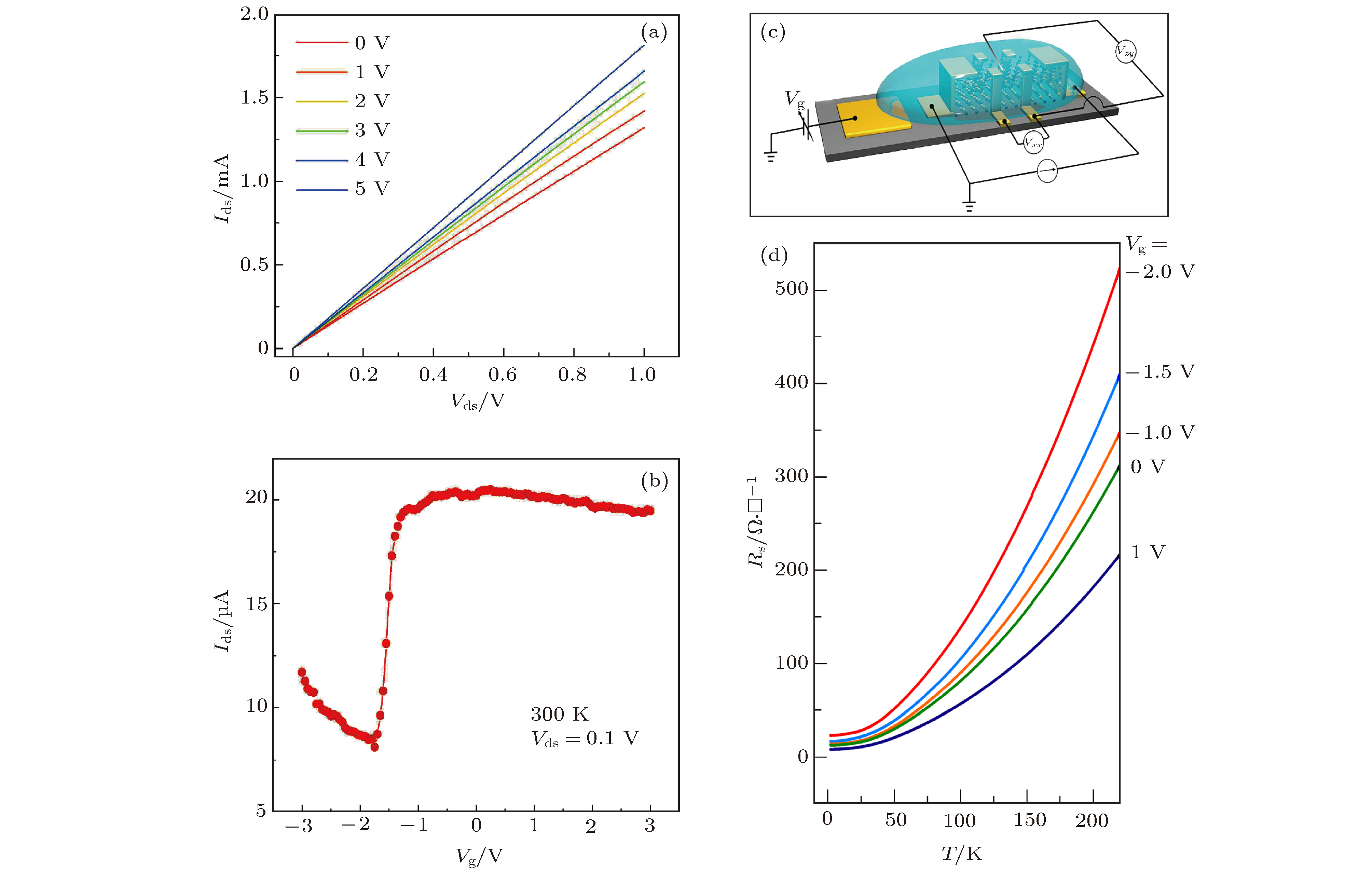
图 9 基于CdTe/PbTe(111)异质结的EDL-FET (a)输出特性曲线和(b)转移特性曲线; (c) EDL-FET结构示意图; (d)不同栅压下的面电阻和温度的依赖关系[22]
Figure 9. The output characteristic (a) and (b) transfer characteristic of the EDL-FET based on CdTe/PbTe(111) heterojunction; (c) the schematic diagram of the EDL-FET structure; (d) temperature dependence of sheet resistance RS at selected gate voltages[22].
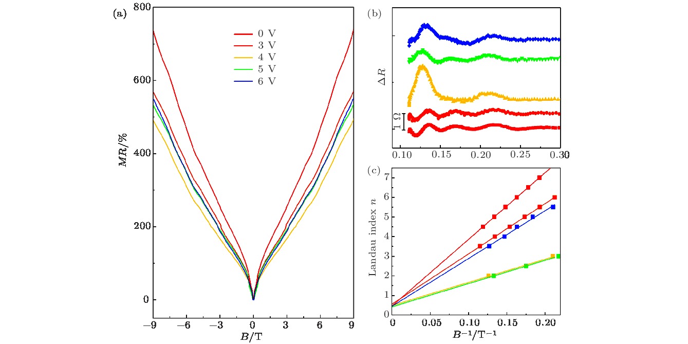
图 10 (a) 2 K温度下不同栅压对应的磁阻; (b)栅压调控下SdH振荡的振幅和周期变化; (c)不同栅压下的SdH振荡的朗道能级线性拟合[22]
Figure 10. Gate-tunable SdH oscillation in 2DEG: (a) Magnetoresistance measured under perpendicular magnetic field at 2 K with various gate voltages; (b) SdH oscillations versus 1/B after subtracting the background, showing systematic changes to the oscillation amplitude and period with gate voltage; (c) a Landau fan diagram for SdH oscillation at different gate voltages[22].
图 11 (a) PbTe薄膜的拉曼谱图; (b) 30 nm厚度的CdTe覆层的CdTe/PbTe(111)异质结的拉曼谱图(绿色线), 内插图为BaF2衬底上直接生长50 nm CdTe层的拉曼谱; 为了便于直接对比, 图中也给出了PbTe样品的拉曼谱图(红线)[20]
Figure 11. (a) Raman shifts for an epitaxial PbTe reference sample, multiple optical phonon modes dominate the spectral profile; (b) raman shifts for a CdTe/PbTe(111) HJ with 30 nm CdTe capping layer (green line), the inset is a Raman spectrum for a 50 nm CdTe layer on a BaF2 substrate. For direct comparison, the Raman shift of the reference PbTe film is plotted in a red line[20].
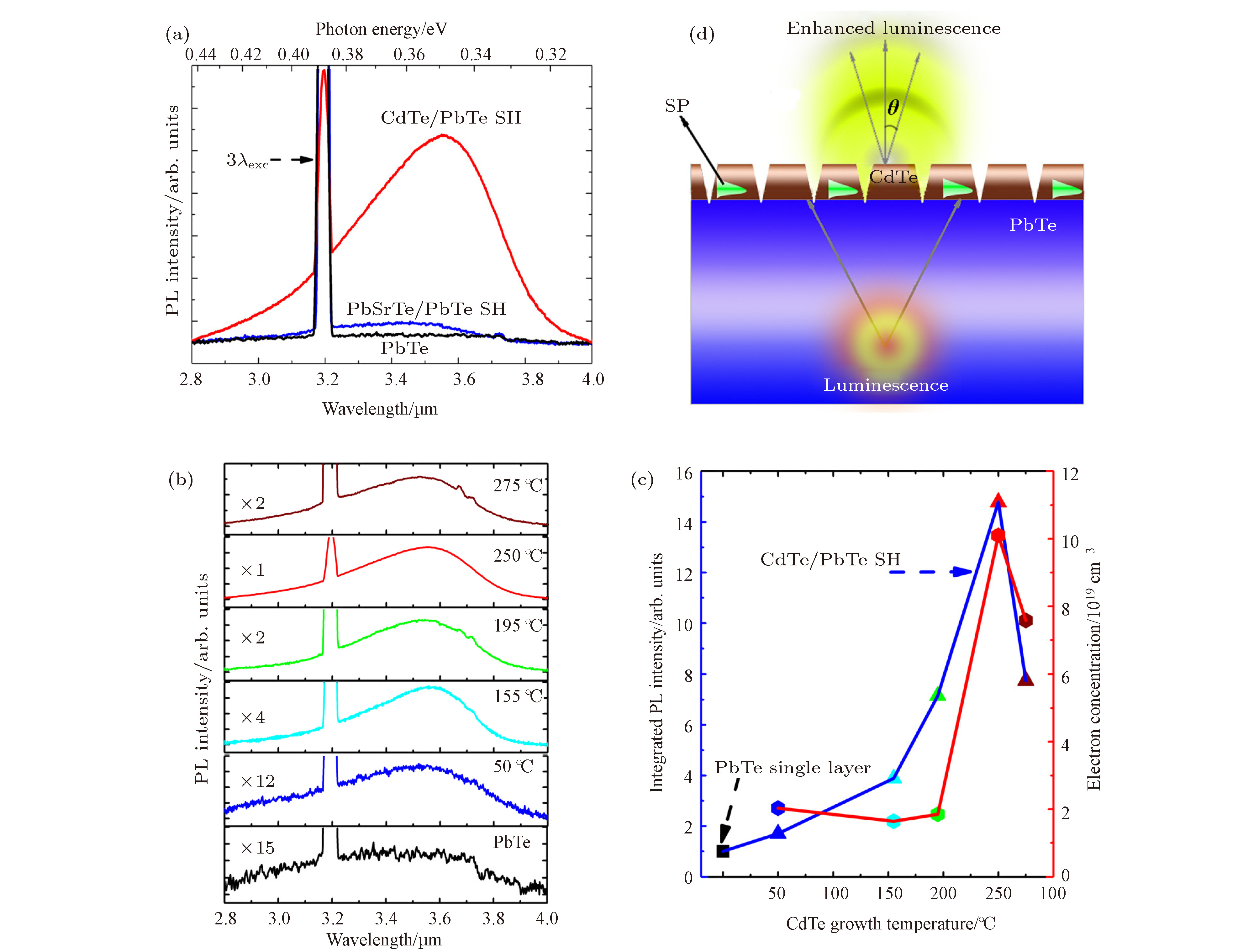
图 12 (a) CdTe/PbTe单异质结样品、PbTe体材料样品和PbSrTe/PbTe单异质结样品的PL谱, 图中3.2 μm处的尖峰是1.064 μm激光的散射光; (b)不同CdTe生长温度的CdTe/PbTe单异质结的PL谱; (c)CdTe/PbTe单异质结PL积分强度以及实验测得的电子浓度随CdTe生长温度变化曲线; (d)SP与中红外光子耦合增强PL效应的示意图[17]
Figure 12. (a) Comparison of three typical MIR PL spectra measured at room temperature for a CdTe/PbTe single heterojunction (SH), a PbSrTe/PbTe SH, and a PbTe single layer; (b) MIR PL for CdTe/PbTe SHs with different CdTe growth temperature TCdTe; (c) integrated PL intensities derived from (b) and electron densities of the SHs measured by Hall effect versus TCdTe, the square symbol represents PL intensity from a PbTe single layer; (d) schematic representation of CdTe/PbTe for plasmonic enhancement of MIR emission[17].
图 13 (a) CdTe/PbTe异质结探测器的俯视图和侧视图; (b)室温时探测器在不同偏压下的红外响应光谱; (c)探测器在不同波长脉冲激光下的脉冲响应; (d)探测器的时间分辨响应
Figure 13. (a) Top-view and side-view of the CdTe/PbTe heterojunction photodetector; (b) the photoresponse spectra of the photodetector under different bias voltages at room temperature; (c) implusephotoresponses under laser of different wavelengths; (d) time-resolved photoresponse.
-
[1] Bardeen J, Brattain W H 1948 Phys. Rev. 74 230
 Google Scholar
[2] Brattain W H, Bardeen J 1948 Phys. Rev. 74 231
 Google Scholar
[3] Nakamura S, Mukai T, Senoh M 1994 Appl. Phys. Lett. 64 1687
 Google Scholar
[4] Klitzing K V, Dorda G, Pepper M 1980 Phys. Rev. Lett. 45 494
 Google Scholar
[5] König M, Wiedmann S, Brüne C, Roth A, Buhmann H, Molenkamp L W, Qi X L, Zhang S C 2007 Science 318 766
 Google Scholar
[6] Cao Y, Fatemi V, Fang S, Watanabe K, Taniguchi T, Kaxiras E, Jarillo-Herrero P 2018 Nature 556 43
 Google Scholar
[7] Rogalski A 2012 Opto-Electronics Review 20 279
[8] Springholz G, Ueta A Y, Frank N, Bauer G 1996 Appl. Phys. Lett. 69 2822
 Google Scholar
[9] Yuan S, Springholz G, Bauer G, Kriechbaum M 1994 Phys. Rev. B 49 5476
 Google Scholar
[10] Rahim M, Arnold M, Felder F, Behfar K, Zogg H 2007 Appl. Phys. Lett. 91 151102
 Google Scholar
[11] Koga T, Harman T C, Cronin S B, Dresselhaus M S 1999 Phys. Rev. B 60 14286
 Google Scholar
[12] Casian A, Sur I, Scherrer H, Dashevsky Z 2000 Phys. Rev. B 61 15965
 Google Scholar
[13] Koike K, Honden T, Makabe I, Yan F P, Yano M 2003 J. Cryst. Growth 257 212
 Google Scholar
[14] Heiss W, Groiss H, Kaufmann E, Hesser G, Böberl M, Springholz G, Schäffler F, Koike K, Harada H, Yano M 2006 Appl. Phys. Lett. 88 192109
 Google Scholar
[15] Hasegawa M M, de Andrada e Silva E A 2003 Phys. Rev. B 68 205309
 Google Scholar
[16] Si J, Jin S, Zhang H, Zhu P, Qiu D, Wu H 2008 Appl. Phys. Lett. 93 202101
 Google Scholar
[17] Cai C, Jin S, Wu H, Zhang B, Hu L, McCann P J 2012 Appl. Phys. Lett. 100 182104
 Google Scholar
[18] Jin S, Cai C, Bi G, Zhang B, Wu H, Zhang Y 2013 Phys. Rev. B 87 235315
 Google Scholar
[19] Jin S, Cai C, Zhang B, Wu H, Bi G, Si J, Zhang Y 2012 New J. Phys. 14 113021
 Google Scholar
[20] Zhang B, Cai C, Zhu H, Wu F, Ye Z, Chen Y, Li R, Kong W, Wu H 2014 Appl. Phys. Lett. 104 161601
 Google Scholar
[21] Zhang B, Lu P, Liu H, Jiao L, Ye Z, Jaime M, Balakirev F F, Yuan H, Wu H, Pan W, Zhang Y 2015 Nano Lett. 15 4381
 Google Scholar
[22] Zhang L, Shu T, Wu H, Ye Z, Zhu L 2019 Phys. Status Solidi 13 1800551
 Google Scholar
[23] Mascarenhas A 2012 Spontaneous Ordering in Semiconductor Alloys (Springer Science & Business Media)
[24] Suzuki K, Seto S, Sawada T, Imai K 2002 IEEE Trans. Nucl. Sci. 49 1287
 Google Scholar
[25] Waghmare U V, Spaldin N A, Kandpal H C, Seshadri R 2003 Phys. Rev. B 67 125111
 Google Scholar
[26] Božin E S, Malliakas C D, Souvatzis P, Proffen T, Spaldin N A, Kanatzidis M G, Billinge S J L 2010 Science 330 1660
 Google Scholar
[27] Su C H 2008 J. Appl. Phys. 103 084903
 Google Scholar
[28] Segall B, Lorenz M R, Halsted R E 1963 Phys. Rev. 129 2471
 Google Scholar
[29] Bissert G, Hesse K F 1978 Acta Crystallographica Section B 34 1322
 Google Scholar
[30] van de Walle C G, Martin R M 1987 Phys. Rev. B 35 8154
 Google Scholar
[31] Hiyamizu S, Mimura T, Fujii T, Nanbu K, Hashimoto H 1981 Jpn. J. Appl. Phys. 20 L245
 Google Scholar
[32] Ismail K, Meyerson B S, Wang P J 1991 Appl. Phys. Lett. 58 2117
 Google Scholar
[33] Kikkawa J M, Smorchkova I P, Samarth N, Awschalom D D 1997 Science 277 1284
 Google Scholar
[34] Madelung O 2012 Semiconductors: Data Handbook (Springer Science & Business Media)
[35] Ando Y 2013 J. Phys. Soc. Jpn. 82 102001
 Google Scholar
[36] Hsieh T H, Lin H, Liu J, Duan W, Bansil A, Fu L 2012 Nat. Commun. 3 982
 Google Scholar
[37] Ma S, Guo C, Xiao C, Wu F, Smidman M, Lu Y, Yuan H, Wu H 2018 Adv. Funct. Mater. 28 1803188
 Google Scholar
[38] Miao M S, Yan Q, van de Walle C G, Lou W K, Li L L, Chang K 2012 Phys. Rev. Lett. 109 186803
 Google Scholar
[39] Ueno K, Shimotani H, Yuan H, Ye J, Kawasaki M, Iwasa Y 2014 J. Phys. Soc. Jpn. 83 032001
 Google Scholar
[40] Lei B, Wang N Z, Shang C, Meng F B, Ma L K, Luo X G, Wu T, Sun Z, Wang Y, Jiang Z, Mao B H, Liu Z, Yu Y J, Zhang Y B, Chen X H 2017 Phys. Rev. B 95 020503
 Google Scholar
[41] Amirtharaj P M, Pollak F H 1984 Appl. Phys. Lett. 45 789
 Google Scholar
[42] Tian Z, Garg J, Esfarjani K, Shiga T, Shiomi J, Chen G 2012 Phys. Rev. B 85 184303
 Google Scholar
[43] Venkatasubramanian R, Siivola E, Colpitts T, O'Quinn B 2001 Nature 413 597
 Google Scholar
[44] Pei Y, LaLonde A D, Heinz N A, Snyder G J 2012 Adv. Energy Mater. 2 670
 Google Scholar
Catalog
Metrics
- Abstract views: 25459
- PDF Downloads: 489
- Cited By: 0


 DownLoad:
